GS6001 6002 6004 聚洵低功耗运算放大器
聚洵低功耗运算放大器GS8551 GS8552 GS8554

描述:GS8551/GS8552/GS8554放大器是单/双/四电源,微功耗,零漂移CMOS运算放大器,这些放大器提供1.8MHz的带宽,轨至轨输入和输出以及1.8V至5.5V的单电源供电。
GS855X使用斩波稳定技术来提供非常低的失调电压(最大值小于5µV),并且在整个温度范围内漂移接近零。
每个放大器的静态电源电流低至180µA,输入偏置电流极低,仅为20pA,因此该器件是低失调,低功耗和高阻抗应用的理想选择。
GS855X提供了出色的CMRR,而没有与传统的互补输入级相关的分频器。
该设计为驱动模数转换器带来了卓越的性能转换器(ADC),而不会降低差分线性度。
GS8551提供SOT23-5和SOP-8封装。
GS8552提供MSOP-8和SOP-8封装。
GS8554 Quad具有绿色SOP-14和TSSOP-14封装。
在所有电源电压下,-45oC至+ 125oC的扩展温度范围提供了额外的设计灵活性。
特点:+ 1.8V〜+ 5.5V单电源供电•嵌入式RF抗EMI滤波器•轨到轨输入/输出•小型封装:•增益带宽乘积:1.8MHz(典型@ 25°C)GS8551采用SOT23-5和SOP-8封装•低输入偏置电流:20pA(典型值@ 25°C)GS8552采用MSOP-8和SOP-8封装•低失调电压:30µV(最大@ 25°C)GS8554采用SOP-14和TSSOP-14封装•静态电流:每个放大器180µA(典型值)•工作温度:-45°C〜+ 125°C•零漂移:0.03µV / oC(典型值)应用:换能器应用•手持测试设备•温度测量•电池供电的仪器•电子秤Features•Single-Supply Operation from +1.8V ~ +5.5V •Embedded RF Anti-EMI Filter•Rail-to-Rail Input / Output •Small Package:•Gain-Bandwidth Product: 1.8MHz (Typ. @25°C) GS8551 Available in SOT23-5 and SOP-8 Packages•Low Input Bias Current: 20pA (Typ. @25°C) GS8552 Available in MSOP-8 and SOP-8 Packages•Low Offset Voltage: 30µV (Max. @25°C) GS8554 Available in SOP-14 and TSSOP-14 Packages•Quiescent Current: 180µA per Amplifier (Typ)•Operating Temperature: -45°C ~ +125°C•Zero Drift: 0.03µV/o C (Typ)General DescriptionGS8551 / GS8552 / GS8554放大器是单/双/四电源,微功耗,零漂移CMOS运算放大器,这些放大器提供1.8MHz的带宽,轨至轨输入和输出以及1.8以上的单电源供电V至5.5V。
聚洵低功耗运算放大器GS8591 8592 8594

GS8591/GS8592/GS8594放大器是单/双/四电源,微功耗,零漂移CMOS运算放大器,这些放大器提供4.5MHz的带宽,轨至轨输入和输出以及1.8V至5.5V的单电源供电。
GS859X使用斩波稳定技术来提供非常低的失调电压(最大值小于50µV),并且在整个温度范围内漂移接近零。
每个放大器550µA的低静态电源电流和20pA的极低输入偏置电流使这些器件成为低失调,低功耗和高阻抗应用的理想选择。
GS859X提供了出色的CMRR,而没有与传统的互补输入级相关的分频器。
这种设计在驱动模数转换器(ADC)方面具有卓越的性能,而不会降低差分线性度。
GS8591提供SOT23-5和SOP-8封装。
GS8592提供MSOP-8和SOP-8封装。
GS8594 Quad具有绿色SOP-14和TSSOP-14封装。
在所有电源电压下,-45oC 至+ 125oC的扩展温度范围提供了额外的设计灵活性。
特性:+ 1.8V〜+ 5.5V单电源供电•嵌入式RF抗EMI滤波器•轨到轨输入/输出•小型封装:•增益带宽乘积:4.5MHz(典型@ 25°C)GS8591采用SOT23-5和SOP-8封装•低输入偏置电流:20pA(典型值@ 25°C)GS8592采用MSOP-8和SOP-8封装•低失调电压:30µV(最大@ 25°C)GS8594采用SOP-14和TSSOP-14封装•静态电流:每个放大器550µA(典型值)•工作温度:-45°C〜+ 125°C•零漂移:0.03µV / oC(典型值)Features•Single-Supply Operation from +1.8V ~ +5.5V •Embedded RF Anti-EMI Filter•Rail-to-Rail Input / Output •Small Package:•Gain-Bandwidth Product: 4.5MHz (Typ. @25°C) GS8591 Available in SOT23-5 and SOP-8 Packages•Low Input Bias Current: 20pA (Typ. @25°C) GS8592 Available in MSOP-8 and SOP-8 Packages•Low Offset Voltage: 30µV (Max. @25°C) GS8594 Available in SOP-14 and TSSOP-14 Packages •Quiescent Current: 550µA per Amplifier (Typ.)•Operating Temperature: -45°C ~ +125°C•Zero Drift: 0.03µV/o C (Typ.)General DescriptionThe GS859X amplifier is single/dual/quad supply, micro-power, zero-drift CMOS operational amplifiers, the amplifiers offer bandwidth of 4.5MHz, rail-to-rail inputs and outputs, and single-supply operation from 1.8V to 5.5V. GS859X uses chopper stabilized technique to provide very low offset voltage (less than 50µV maximum) and near zero drift over temperature. Low quiescent supply current of 550µA per amplifier and very low input bias current of 20pA make the devices an ideal choice for low offset, low power consumption and high impedance applications. The GS859X offers excellent CMRR without the crossover associated with traditional complementary input stages. This design results in superior performance for driving analog-to-digital converters (ADCs) without degradation of differential linearity.The GS8591 is available in SOT23-5 and SOP-8 packages. And the GS8592 is available in MSOP-8 and SOP-8 packages. TheGS8594 Quad is available in Green SOP-14 and TSSOP-14 packages. The extended temperature range of -45o C to +125o C over all supply voltages offers additional design flexibility.Applications•Transducer Application •Handheld Test Equipment•Temperature Measurements •Battery-Powered Instrumentation•Electronics ScalesPin ConfigurationFigure 1. Pin Assignment DiagramAbsolute Maximum RatingsCondition Min Max Power Supply Voltage (V DD to Vss) -0.5V +7.5V Analog Input Voltage (IN+ or IN-) Vss-0.5V V DD+0.5V PDB Input Voltage Vss-0.5V +7V Operating Temperature Range -45°C +125°C Junction Temperature +160°CStorage Temperature Range -55°C +150°C Lead Temperature (soldering, 10sec) +260°CPackage Thermal Resistance (T A=+25 )SOP-8, θJA 125°C/WMSOP-8, θJA 216°C/WSOT23-5, θJA 190°C/WESD SusceptibilityHBM 6KVMM 400VNote: Stress greater than those listed under Absolute Maximum Ratings may cause permanent damage to the device. This is a stress rating only and functional operation of the device at these or any other conditions outside those indicated in the operational sections of this specification are not implied. Exposure to absolute maximum rating conditions for extended periods may affect reliability.Package/Ordering InformationMODEL CHANNEL ORDER NUMBERPACKAGEDESCRIPTIONPACKAGEOPTIONMARKINGINFORMATIONGS8591 SingleGS8591-TR SOT23-5 Tape and Reel,3000 8591 GS8591Y-SR SOP-8 Tape and Reel,4000 GS8591YGS8592 Dual G S8592-SR SOP-8 Tape and Reel,4000 GS8592 GS8592-MR MSOP-8 Tape and Reel,3000 GS8592GS8594 Quad GS8594-TR TSSOP-14 Tape and Reel,3000 GS8594 GS8594-SR SOP-14 Tape and Reel,2500 GS8594Electrical Characteristics(V S = +5V, V CM = +2.5V, V O = +2.5V, T A = +25 , unless otherwise noted.)PARAMETER CONDITIONS MIN TYP MAX UNITS INPUT CHARACTERISTICSInput Offset Voltage (V OS) 1 5 µV Input Bias Current (I B) 20 pA Input Offset Current (I OS) 10 pA Common-Mode Rejection Ratio(CMRR)V CM = 0V to 5V 110 dB Large Signal Voltage Gain ( A VO) R L = 10kΩ, V O = 0.3V to 4.7V 145 dB Input Offset Voltage Drift (∆V OS/∆T) 30 nV/ OUTPUT CHARACTERISTICSOutput Voltage High (V OH) R L = 100kΩ to - V S 4.998 V R L = 10kΩ to - V S 4.994 VOutput Voltage Low (V OL) R L = 100kΩ to + V S 2 mV R L = 10kΩ to + V S 5 mVShort Circuit Limit (I SC) R L =10Ω to - V S 43 mA Output Current (I O) 30 mA POWER SUPPLYPower Supply Rejection Ratio (PSRR) V S = 2.5V to 5.5V 115 dB Quiescent Current (I Q) V O = 0V, R L = 0Ω 180 µA DYNAMIC PERFORMANCEGain-Bandwidth Product (GBP) G = +100 4.5 MHz Slew Rate (SR) R L = 10kΩ 2.5 V/µs Overload Recovery Time 0.10 ms NOISE PERFORMANCEVoltage Noise (e n p-p) 0Hz to 10Hz 0.2 µV P-PnV Voltage Noise Density (e n) f = 1kHz 30 HzTypical Performance characteristicsLarge Signal Transient Response at +5V Large Signal Transient Response at +2.5VC L=300pF R L=2kΩA V=+1C L=300pFR L=2kΩA V=+1Time(4µs/div) Time(2µs/div)Small Signal Transient Response at +5V Small Signal Transient Response at +2.5VC L=50pF R L=∞A V=+1C L=50pFR L=∞A V=+1Time(4µs/div) Time(4µs/div)Closed Loop Gain vs. Frequency at +5V Closed Loop Gain vs. Frequency at +2.5V G=-100 G=-100 G=-10 G=-10G=+1 G=+1Frequency (kHz) Frequency (kHz)Typical Performance characteristicsOpen Loop Gain, Phase Shift vs. Frequency at +5V Open Loop Gain, Phase Shift vs. Frequency at +2.5VPhase ShiftV L=0pFR L=∞V L=0pFR L=∞Phase ShiftOpen Loop GainOpen Loop Gain Frequency (Hz) Frequency (Hz) Positive Overvoltage Recovery Negative Overvoltage RecoveryV SY= 2.5VV IN=-200mVp-p(RET to GND)C L=0pFR L=10kΩA V=-100 V SY= 2.5VV IN=-200mVp-p(RET to GND) C L=0pFR L=10kΩA V=-100Time (40µs/div) Time (40µs/div) 0.1Hz to 10Hz Noise at +5V 0.1Hz to 10Hz Noise at +2.5VG=10000G=10000 Time (10s/div) Time (10s/div)Application NoteSizeGS859X系列运算放大器具有单位增益稳定的特性,适用于各种通用应用。
奥伟斯科技为您提供GS8051_GS8052_GS8054系列聚洵高速运算放大器

GS8051/GS8052/GS8054描述:GS8051 / 1N(单),GS8052 / 2N(双),GS8054(四)是轨到轨输出电压反馈放大器,具有易用性和低成本。
它们具有通常在电流反馈放大器中发现的带宽和压摆率。
GS8051系列均具有宽的输入共模电压范围和输出电压摆幅,因此易于在低至2.5V的单电源上使用。
尽管成本较低,但GS8051系列仍具有出色的整体性能。
它们提供250MHz(G = +1)的宽带宽,以及高达52MHz(G = +2)的0.1dB平坦度,并提供典型的2.8mA /放大器低功耗。
GS8051系列具有低失真和快速建立的特点,非常适合于缓冲高速A / D或D / A转换器。
GS8051 / 2N具有掉电禁用功能,可将电源电流降至50µA。
这些功能使GS8051 / 2N成为尺寸和功耗至关重要的便携式和电池供电应用的理想选择。
所有参数均在-40至+125扩展温度范围内指定。
特点:+ 2.5V〜+ 5.5V单电源供电GS8051提供SOT23-5和SC70-5封装•轨到轨输出GS8052提供SOP-8和MSOP-8封装•-3dB带宽(G = + 1):250MHz(典型值)GS8054提供SOP-14和TSSOP-14封装•低输入偏置电流:1pA(典型值)GS8051N提供SOT23-6和SC70-6封装•静态电流:2.8mA /放大器(典型值)GS8052N采用MSOP-10封装•工作温度:-40°C〜+ 125°C•小包装:Features•+ 2.5V〜+ 5.5V单电源供电轨到轨输出-3dB带宽(G = + 1):250MHz(Typ。
)低输入偏置电流:1pA(典型值)静态电流:2.8mA /放大器(典型值)工作温度:-40°C〜+ 125°C 小包装:GS8051提供SOT23-5和SC70-5封装GS8052提供SOP-8和MSOP-8封装GS8054提供SOP-14和TSSOP-14封装GS8051N提供SOT23-6和SC70-6封装GS8052N采用MSOP-10封装:General DescriptionGS8051 / 1N(单),GS8052 / 2N(双),GS8054(四)是轨到轨输出电压反馈放大器,具有易用性和低成本。
MAX44242 低输入偏置电流、低噪声操作放大器 (OP 放大器) 评估套件说明书

General DescriptionThe MAX44242 evaluation kit (EV kit) provides a prov-en design to evaluate the MAX44242 low-input biascurrent, low-noise operational amplifier (op amp) in an8-pin µMAX ® package. The EV kit circuit is preconfig-ured as noninverting amplifiers, but can be adapted toother topologies by changing a few components. Thecomponent pads accommodate 0805 packages, makingthem easy to solder and replace. The EV kit comes with aMAX44242AUA+ installed.Features and Benefits●Accommodates Multiple Op-Amp Configurations●Rail-to-Rail Outputs●Accommodates Easy-to-Use 0805 Components● 2.7V to 20V Single Supply or ±1.35V to Q 10V DualSupplies●Proven PCB Layout●Fully Assembled and TestedQuick StartRequired Equipment●MAX44242 EV kit●+5V, 10mA DC power supply (PS1)●Two precision voltage sources●Two digital multimeters (DMMs)Procedure The EV kit is fully assembled and tested. Follow the steps below to verify board operation:1) Verify that the jumpers are in their default position, as shown in Table 1.2) Connect the positive terminal of the +5V supply to VDD and the negative terminal to GND and VSS.3) Connect the positive terminal of the precision voltage source to INAP . Connect the negative terminal of the precision voltage source to GND.4) Connect INAM to GND.5) Connect the positive terminal of the second precision voltage source to the INBP pad. Connect the nega-tive terminal of the precision voltage source to GND.6) Connect INBM to GND.7) Connect the DMMs to monitor the voltages on OUTA and OUTB. With the 10kΩ feedback resistors and 1kΩ series resistors, the gain of each noninverting amplifier is +11.8) Turn on the +5V power supply.9) Apply 100mV from the precision voltage sources. Observe the output at OUTA and OUTB on the DMMs. Both should read approximately +1.1V.10) Apply 400mV from the precision voltage sources. Both OUTA and OUTB should read approximately +4.4V.19-6917; Rev 0; 2/14Ordering Information appears at end of data sheet.μMAX is a registered trademark of Maxim Integrated Products, Inc.Detailed Description of HardwareThe MAX44242 EV kit provides a proven layout for theMAX44242 low input bias current, low-noise dual op amp.The IC is a single-supply dual op amp whose primaryapplication is operating in the noninverting configuration;however, the IC can operate with a dual supply as long asthe voltage across the VDD and GND pins of the IC do notexceed the absolute maximum ratings. When operatingwith a single supply, short VSS to GND.Op-Amp Configurations The IC is a single-supply dual op amp ideal for differential sensing, noninverting amplification, buffering, and filter-ing. A few common configurations are shown in the next few sections.The following sections explain how to configure one of the device’s op amps (op-amp A). To configure the device’s second op amp (op-amp B), the same equations can be used after modifying the component reference designa-tors. For op-amp B, the equations should be modified by adding 10 to the number portion of the reference designa-tors (e.g., for the noninverting configuration, equation R1 becomes R11 and R5 becomes R15).Noninverting ConfigurationThe EV kit comes preconfigured as a noninvertingamplifier. The gain is set by the ratio of R5 and R1. TheEV kit comes preconfigured for a gain of +11. The outputvoltage for the noninverting configuration is given by the equation below:OUTA INAP R5V 1V R1 =+ *Default position.JUMPERSHUNT POSITION DESCRIPTION JU1Installed*Connects INAM to R1. Also shorts capacitor C5.OpenConnects INAM to R1 through capacitor C5. When AC-coupling is desired, remove the shunt and install capacitor C5. JU2Installed*Connects INAP to JU3 position 1. Also shorts capacitor C6. OpenConnects INAP to JU3 position 1 through capacitor C6. When AC-coupling is desired, remove the shunt and install capacitor C6. JU31-2*Connects INAP to JU2 and C6 through R2 and R82-3Connects INAP to GND through R2 and R8JU4Installed*Connects OUTA to OUTA OpenConnects OUTA to OUTA through capacitor C10. When AC-coupling is desired, remove the shunt and install capacitor C10. JU5Installed*Connects INBM to R11. Also shorts capacitor C15. OpenConnects INBM to R11 through capacitor C15. When AC-coupling is desired, remove the shunt and install capacitor C15. JU6Installed*Connects INBP to JU6 position 1. Also shorts capacitor C16. OpenConnects INBP to JU6 position 1 through capacitor C16. When AC-coupling is desired, remove the shunt and install capacitor C16. JU71-2*Connects INBP to JU7 and C16 through R12 and R182-3Connects INBP to GND through R12 and R18JU8Installed*Connects OUTB to OUTB Open Connects OUTB to OUTB through capacitor C20. When AC-coupling is desired, remove the shunt and install capacitor C20.R1–R3, and R5 with appropriate resistors. WhenR1 = R2 and R3 = R5, the CMRR of the differential ampli-fier is determined by the matching of the resistor ratiosR1/R2 and R3/R5.OUTA INAP INAM V GAIN (V V )=−where:R5R3GAIN R1R2==Sallen-Key Filter ConfigurationThe Sallen-Key filter topology is ideal for filtering sensorsignals with a second-order filter and acting as a buffer.Schematic complexity is reduced by combining the filterand buffer operations. The EV kit can be configured ina Sallen-Key topology by replacing and populating afew components. The Sallen-Key topology is typicallyconfigured as a unity-gain buffer, which can be done byreplacing R1 and R5 with 0Ω resistors and short JU2. Thenoninverting signal is applied to the INAP test point withJU2 short and short pins 1-2 on JU3 or do the same on theINBP pad similarly. The filter component pads are R2–R4,and R8, where some have to be populated with resistorsand others with capacitors.Lowpass Sallen-Key FilterTo configure the Sallen-Key as a lowpass filter, populatethe R2 and R8 pads with resistors, and populate the R3and R4 pads with capacitors. The corner frequency and Qare then given by:C R3R2R8f Q ==the R3 and R4 pads with resistors and populate the R2 and R8 pads with capacitors. The corner frequency and Qare then given by:C R4R2R8f Q ==Transimpedance Application To configure op-amp U1-A as a transimpedance amplifier (TIA), replace R1 with a 0Ω resistor and install a shunt on jumper JU1 and shunt on pins 2-3 on jumper JU3. The output voltage of the TIA is the input current multiplied by the feedback resistor:OUT IN BIAS OS V (I I )R4V =+×+where R4 is installed as a 10kΩ resistor, I IN is defined as the input current source applied at the INAM pad, I BIAS is the input bias current, and V OS is the input offset voltage of the op amp. Use capacitor C8 (and C7, if applicable) to stabilize the op amp by rolling off high-frequency gain due to a large cable capacitance. Similarly, we can configure op-amp U1-B for transimpedance application.Capacitive Loads Some applications require driving large capacitive loads. To improve the stability of the amplifier, replace R6 (R16 for U1-B) with a suitable resistor value to improve ampli-fier phase margin. The R6/C9 (R16/C19 for U1-B) filter can also be used as an anti-alias filter, or to limit amplifier output noise by reducing its output bandwidth.DESIGNATION QTY DESCRIPTIONC1, C320.1µF ±10%, 25V X7R ceramic capacitors (0805)C2, C424.7µF ±10%, 25V X5R ceramic capacitors (0805)C5–C10, C15–C200Not installed, ceramic capacitors(0805)GND2Black test points INAM, INAP,INBM, INBP,OUTA, OUTB,VDD, VSS8Red test pointsJU1, JU2,JU4–JU6, JU862-pin headers JU3, JU723-pin headers DESIGNATION QTY DESCRIPTION R1, R2,R11, R1241kΩ ±1% resistors (0805)R3, R4, R7,R13, R14, R170Not installed, resistors (0805) R5, R15210kΩ ±1% resistors (0805)R6, R8,R16, R1840Ω ±5% resistors (0805) TP1, TP20Not installed, miniature test points U11Dual low-power, rail-to-rail I/O opamp (8 µMAX)Maxim MAX44242AUA+—8Shunts—1PCB: MAX44242 EVKITFigure 1. MAX44242 EV Kit SchematicFigure 3. MAX44242 EV Kit PCB Layout—Component SideComponent SideFigure 4. MAX44242 EV Kit PCB Layout—Solder SidePART TYPE MAX44242EVKIT#EV Kit #Denotes ROHS compliant.Maxim Integrated cannot assume responsibility for use of any circuitry other than circuitry entirely embodied in a Maxim Integrated product. No circuit patent licenses are implied. Maxim Integrated reserves the right to change the circuitry and specifications without notice at any time.REVISIONNUMBERREVISION DATE DESCRIPTION PAGES CHANGED 02/14Initial release —For pricing, delivery, and ordering information, please contact Maxim Direct at 1-888-629-4642, or visit Maxim Integrated’s website at .。
GS358 聚洵低功耗运放
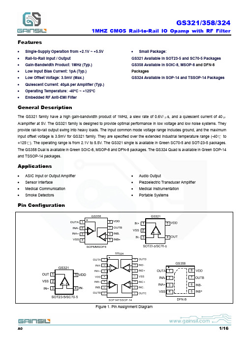
GS321/358/324 1MHZ CMOS Rail-to-Rail IO Opamp with RF FilterFeatures•Single-Supply Operation from +2.1V ~ +5.5V •Rail-to-Rail Input / Output•Gain-Bandwidth Product: 1MHz (Typ.) •Low Input Bias Current: 1pA (Typ.)•Low Offset Voltage: 3.5mV (Max.) •Quiescent Current: 40µA per Amplifier (Typ.) •Operating Temperature: -40°C ~ +125°C •Embedded RF Anti-EMI Filter •Small Package:GS321 Available in SOT23-5 and SC70-5 Packages GS358 Available in SOIC-8, MSOP-8 and DFN-8 PackagesGS324 Available in SOP-14 and TSSOP-14 PackagesGeneral DescriptionThe GS321 family have a high gain-bandwidth product of 1MHz, a slew rate of 0.6V/μs, and a quiescent current of 40μA/amplifier at 5V. The GS321 family is designed to provide optimal performance in low voltage and low noise systems. They provide rail-to-rail output swing into heavy loads. The input common mode voltage range includes ground, and the maximum input offset voltage is 3.5mV for GS321 family. They are specified over the extended industrial temperature range (-40℃to +125℃). The operating range is from 2.1V to 5.5V. The GS321 single is available in Green SC70-5 and SOT-23-5 packages. The GS358 Dual is available in Green SOIC-8, MSOP-8 and DFN-8 packages. The GS324 Quad is available in Green SOP-14 and TSSOP-14 packages.Applications•ASIC Input or Output Amplifier •Sensor Interface•Medical Communication •Smoke Detectors •Audio Output•Piezoelectric Transducer Amplifier •Medical Instrumentation •Portable SystemsPin ConfigurationFigure 1. Pin Assignment DiagramAbsolute Maximum RatingsCondition Min MaxPower Supply Voltage (V DD to Vss) -0.5V +7.5VAnalog Input Voltage (IN+ or IN-) Vss-0.5V V DD+0.5VPDB Input Voltage Vss-0.5V +7V Operating Temperature Range -40°C+125°C Junction Temperature +160°CStorage Temperature Range -55°C+150°CLead Temperature (soldering, 10sec) +260°CPackage Thermal Resistance (T A=+25℃)SOP-8, θJA125°C/WMSOP-8, θJA216°C/WSOT23-5, θJA190°C/WSC70-5, θJA333°C/WESD SusceptibilityHBM 6KVMM 300VNote:Stress greater than those listed under Absolute Maximum Ratings may cause permanent damage to the device. This is a stress rating only and functional operation of the device at these or any other conditions outside those indicated in the operational sections of this specification are not implied. Exposure to absolute maximum rating conditions for extended periods may affect reliability.Package/Ordering InformationMODEL CHANNEL ORDER NUMBERPACKAGEDESCRIPTIONPACKAGEOPTIONMARKINGINFORMATIONGS321 Single GS321-CR SC70-5 Tape and Reel,3000 321 GS321-TR SOT23-5 Tape and Reel,3000 321GS358 Dual GS358-SR SOP-8 Tape and Reel,2500 GS358 GS358-MR MSOP-8 Tape and Reel,3000 GS358 GS358-FR DFN-8 Tape and Reel,3000 GS358GS324 Quad GS324-TR TSSOP-14 Tape and Reel,3000 GS324 GS324-SR SOP-14 Tape and Reel,2500 GS324Electrical Characteristics(At V S = +5V, R L = 100kΩ connected to V S/2, and V OUT = V S/2, unless otherwise noted.)Input Offset Current I OS 1 pA Common-Mode Voltage Range V CM V S = 5.5V -0.1 to +5.6 V Common-Mode Rejection Ratio CMRRV S = 5.5V, V CM = -0.1V to 4V 70 62 62 dBV S = 5.5V, V CM = -0.1V to 5.6V 68 56 55 Open-Loop Voltage Gain A OLR L = 5kΩ, V O = +0.1V to +4.9V 80 70 70 dBR L = 100kΩ, V O = +0.035V to +4.965V 84 80 80 Input Offset Voltage Drift ∆V OS/∆T 2.7 µV/℃OUTPUT CHARACTERISTICSOutput Voltage Swing from Rail V OH R L = 100kΩ 4.997 4.990 4.980 V V OL R L = 100kΩ 3 10 20 mV V OH R L = 10kΩ 4.992 4.970 4.960 V V OL R L = 10kΩ 8 30 40 mVOutput Current I SOURCER = 10Ω to V/284 60 45mATypical Performance characteristicsAt T A =+25oC, V S =+5V, and R L =100KΩ connected to V S /2, unless otherwise noted.Large-Signal Step ResponseSmall-Signal Step ResponseTime (4µs/div)Time (2µs/div)Supply Current vs. Supply VoltageShort-Circuit Current vs. Supply VoltageS u p p l y C u r r e n t (u A )S h o r t -C i r c u i t C u r r e n t (m A )Supply Voltage (V)Supply Voltage (V)Output Voltage vs. Output CurrentOutput Voltage vs. Output CurrentO u t p u t V o l t a g e (V )O u t p u t V o l t a g e(V )Output Current (mA)Output Current (mA)G=+1C L =100pF R L =100KΩG=+1C L =100pF R L =100KΩSourcing CurrentSinking CurrentSourcing CurrentSinking CurrentVs=3VVs=5VO u t p u t V o l t a g e (20m V /d i v )O u t p u t V o l t a g e (500m V /d i v )Typical Performance characteristicsAt T A =+25oC, V S =+5V, and R L =100KΩ connected to V S /2, unless otherwise noted.Overload Recovery TimeSupply Current vs. TemperatureS u p p l y C u r r e n t (µA )Time (2µs/div)Temperature (℃)Input Voltage Noise Spectral Density vs. FrequencyOpen Loop Gain, Phase Shift vs. Frequency at +5VV o l t a g e N o i s e (n V /√H z )O p e n L o o p G a i n (d B )P h a s e S h i f t (D e g r e e s )Frequency (kHz)Frequency (kHz)CMRR vs. FrequencyPSRR vs. FrequencyC M R R (d B )P S R R (d B)Frequency (kHz)Frequency (kHz)Vs=5V G=-5V IN =500mVApplication NoteSizeGS321 family series op amps are unity-gain stable and suitable for a wide range of general-purpose applications. The small footprints of the GS321 family packages save space on printed circuit boards and enable the design of smaller electronic products.Power Supply Bypassing and Board LayoutGS321 family series operates from a single 2.1V to 5.5V supply or dual ±1.05V to ±2.75V supplies. For best performance, a 0.1µF ceramic capacitor should be placed close to the V DD pin in single supply operation. For dual supply operation, both V DD and V SS supplies should be bypassed to ground with separate 0.1µF ceramic capacitors.Low Supply CurrentThe low supply current (typical 40uA per channel) of GS321 family will help to maximize battery life. They are ideal for battery powered systemsOperating VoltageGS321 family operates under wide input supply voltage (2.1V to 5.5V). In addition, all temperature specifications apply from -40 o C to +125 o C. Most behavior remains unchanged throughout the full operating voltage range. These guarantees ensure operation throughout the single Li-Ion battery lifetimeRail-to-Rail InputThe input common-mode range of GS321 family extends 100mV beyond the supply rails (V SS-0.1V to V DD+0.1V). This is achieved by using complementary input stage. For normal operation, inputs should be limited to this range.Rail-to-Rail OutputRail-to-Rail output swing provides maximum possible dynamic range at the output. This is particularly important when operating in low supply voltages. The output voltage of GS321 family can typically swing to less than 5mV from supply rail in light resistive loads (>100kΩ), and 30mV of supply rail in moderate resistive loads (10kΩ).Capacitive Load ToleranceThe GS321 family is optimized for bandwidth and speed, not for driving capacitive loads. Output capacitance will create apole in the amplifier’s feedback path, leading to excessive peaking and potential oscillation. If dealing with load capacitance isa requirement of the application, the two strategies to consider are (1) using a small resistor in series with the amplifier’s output and the load capacitance and (2) reducing the bandwidth of the amplifier’s feedback loop by increasing the overall noise gain. Figure 2. shows a unity gain follower using the series resistor strategy. The resistor isolates the output from the capacitanceFigure 2. Indirectly Driving a Capacitive Load Using Isolation ResistorThe bigger the R ISO resistor value, the more stable V OUT will be. However, if there is a resistive load R L in parallel with the capacitive load, a voltage divider (proportional to R ISO/R L) is formed, this will result in a gain error.The circuit in Figure 3 is an improvement to the one in Figure 2. R F provides the DC accuracy by feed-forward the V IN to R L. C Fand R ISO serve to counteract the loss of phase margin by feeding the high frequency component of the output signal back to the amplifier’s inverting input, thereby preserving the phase margin in the overall feedback loop. Capacitive drive can be increased by increasing the value of C F. This in turn will slow down the pulse response.Figure 3. Indirectly Driving a Capacitive Load with DC AccuracyTypical Application CircuitsDifferential amplifierThe differential amplifier allows the subtraction of two input voltages or cancellation of a signal common the two inputs. It is useful as a computational amplifier in making a differential to single-end conversion or in rejecting a common mode signal. Figure 4. shown the differential amplifier using GS321 family.Figure 4. Differential Amplifier REF12V )()(134321IP IN 144321OUT R R R R R R R R R R R R R R V +++++−=If the resistor ratios are equal (i.e. R 1=R 3 and R 2=R 4), thenREFV )(IN IP 12OUT +−=V V V R RLow Pass Active FilterThe low pass active filter is shown in Figure 5. The DC gain is defined by –R 2/R 1. The filter has a -20dB/decade roll-off after its corner frequency ƒ=1/(2πR C ).Figure 5. Low Pass Active FilterInstrumentation AmplifierThe triple GS321 family can be used to build a three-op-amp instrumentation amplifier as shown in Figure 6. The amplifier in Figure 6 is a high input impedance differential amplifier with gain of R2/R1. The two differential voltage followers assure the high input impedance of the amplifier.Figure 6. Instrument Amplifier.Package Information MSOP8SOP8SOT23-5TSSOP-14SC70-5SOP-14DFN8。
mcp6002i工作原理

mcp6002i工作原理
MCP6002I是一款双运算放大器,它是微芯科技(Microchip Technology)公司生产的一款集成电路。
它主要用于放大电压信号、滤波、比较电压等应用。
MCP6002I的工作原理涉及到运算放大器的
基本原理和特性。
首先,运算放大器是一种差分放大器,它具有高输入阻抗、低
输出阻抗、大增益等特点。
MCP6002I采用双运算放大器设计,意味
着它内部集成了两个独立的运算放大器,可以独立工作,也可以串
联使用。
MCP6002I的工作原理基于运算放大器的反馈网络。
它通常由一
个反馈电阻和一个输入电阻组成,通过这个反馈网络可以实现放大
器的不同功能,比如放大、滤波、比较等。
当输入信号加到运算放
大器的输入端时,根据反馈网络的设计,放大器会对输入信号进行
放大,并输出相应的电压信号。
此外,MCP6002I还具有低功耗、宽工作电压范围、内部电源稳
压器等特点。
它能够在较宽的电压范围内工作,并且在低功耗的情
况下提供稳定的放大功能,适合用于便携式电子设备和电池供电系
统中。
总的来说,MCP6002I的工作原理是基于运算放大器的基本原理和特性,通过反馈网络对输入信号进行放大和处理,同时具有低功耗、宽工作电压范围等特点,适用于各种电子应用中的信号放大和处理。
聚洵低功耗运算放大器GS8331 GS8332 GS834

GS8331 GS8332 GS8334 描述GS8331 GS8332 GS8334放大器是单/双/四电源,微功耗,零漂移CMOS运算放大器,这些放大器提供350 kHz的带宽,轨至轨输入和输出以及1.8V至5.5V的单电源供电。
GS833X使用斩波稳定技术来提供非常低的失调电压(最大值小于10µV),并且在整个温度范围内漂移接近零。
每个放大器具有25µA的低静态电源电流,以及20pA的极低输入偏置电流,使该器件成为低失调,低功耗和高阻抗应用的理想选择。
GS833X提供了出色的CMRR,而没有与传统的互补输入级相关的分频器。
这种设计在驱动模数转换器(ADC)方面具有卓越的性能,而不会降低差分线性度。
GS8331 GS8332 GS8334 应用•换能器应用•手持测试设备•温度测量•电池供电的仪器•电子秤Features•Single-Supply Operation from +1.8V ~ +5.5V •Embedded RF Anti-EMI Filter•Rail-to-Rail Input / Output •Small Package:•Gain-Bandwidth Product: 350KHz (Typ. @25°C) GS8331 Available in SOT23-5, SC70-5 and SOP-8•Low Input Bias Current: 20pA (Typ. @25°C) Packages•Low Offset Voltage: 10uV (Max. @25°C) GS8332 Available in SOP-8, MSOP-8 and DFN-8•Quiescent Current: 25µA per Amplifier (Typ) Packages•Operating Temperature: -45°C ~ +125°C GS8334 Available in SOP-14 and TSSOP-14 Packages•Zero Drift: 0.05µV/°C (Typ)General DescriptionGS833X放大器是单/双/四电源,微功耗,零漂移CMOS运算放大器,这些放大器提供350 kHz的带宽,轨至轨输入和输出以及1.8V至5.5V 的单电源供电。
mcp6001 pdf

PSRR, CMRR (dB) Open-Loop Gain (dB) Open-Loop Phase (°)
100 90 80 70 60 50 40 30 20 1.E1+001
VCM = VSS
PSRR– PSRR+ CMRR
1.E10+002 1.E1k+03 1.1E0+k04 Frequency (Hz)
PSRR, CMRR (dB)
20% 18% 16% 14% 12% 10%
8% 6% 4% 2% 0%
64,695 Samples VCM = VSS
Input Offset Voltage (mV)
图 2-1:
输入失调电压
100
95
90
85
PSRR (VCM = VSS)
80
75
CMRR (VCM = -0.3V to +5.3V)
DS21733E_CN 第 2 页
2005 Microchip Technology Inc.
MCP6001/2/4
AC 特性
电气技术规范:除非另外说明,否则 TA = +25°C, VDD = +1.8 至 5.5V, VSS = GND, VCM = VDD/2, VOUT ≈ VDD/2, RL = 10 kΩ 至 VDD/2 且 CL = 60 pF。
2005 Microchip Technology Inc.
MCP6001/2/4
Percentage of Occurrences -12 -10
注:除非另外说明,否则 TA = +25°C, VDD = +1.8V 至 +5.5V, VSS = GND, VCM = VDD/2, VOUT ≈ VDD/2, RL = 10 kΩ 至 VDD/2 且 CL = 60 pF。
- 1、下载文档前请自行甄别文档内容的完整性,平台不提供额外的编辑、内容补充、找答案等附加服务。
- 2、"仅部分预览"的文档,不可在线预览部分如存在完整性等问题,可反馈申请退款(可完整预览的文档不适用该条件!)。
- 3、如文档侵犯您的权益,请联系客服反馈,我们会尽快为您处理(人工客服工作时间:9:00-18:30)。
GS6001.6002.6004描述GS6001系列的增益带宽乘积为1MHz,转换速率为0.8V /μs,在5V时的静态电流为75μA/放大器。
GS6001系列旨在在低压和低噪声系统中提供最佳性能。
它们可将轨到轨的输出摆幅转换成重负载。
输入共模电压范围包括地,对于GS6001系列,最大输入失调电压为3.5mV。
它们的额定温度范围为扩展的工业温度范围(-40℃至+ 125℃)。
工作范围为1.8V至6V。
GS6001单个采用绿色SC70-5和SOT23-5封装。
GS6002 Dual采用绿色SOP-8和MSOP-8封装。
GS6004 Quad具有绿色SOP-14和TSSOP-14封装。
应用:ASIC输入或输出放大器•传感器接口•医学交流• 烟雾探测器• 音频输出•压电换能器•医疗仪器•便携式系统特征:•+ 1.8V〜+ 6V单电源供电•轨到轨输入/输出•增益带宽乘积:1MHz(典型值)•低输入偏置电流:1pA(典型值)•低失调电压:3.5mV(最大值)•静态电流:每个放大器75µA(典型值)•嵌入式射频抗电磁干扰滤波器•工作温度:-40°C〜+ 125°C•包装:GS6001提供SOT23-5和SC70-5封装GS6002提供SOP-8和MSOP-8封装GS6004提供SOP-14和TSSOP-14封装Features•Single-Supply Operation from +1.8V ~ +6V •Operating Temperature: -40°C ~ +125°C•Rail-to-Rail Input / Output •Small Package:•Gain-Bandwidth Product: 1MHz (Typ.) GS6001 Available in SOT23-5 and SC70-5 Packages •Low Input Bias Current: 1pA (Typ.) GS6002 Available in SOP-8 and MSOP-8 Packages •Low Offset Voltage: 3.5mV (Max.) GS6004 Available in SOP-14 and TSSOP-14 Packages •Quiescent Current: 75µA per Amplifier (Typ.)•Embedded RF Anti-EMI FilterGeneral DescriptionThe GS6001 family have a high gain-bandwidth product of 1MHz, a slew rate of 0.8V/ s, and a quiescent current of 75A/amplifier at 5V. The GS6001 family is designed to provide optimal performance in low voltage and low noise systems. They provide rail-to-rail output swing into heavy loads. The input common mode voltage range includes ground, and the maximum input offset voltage is 3.5mV for GS6001 family. They are specified over the extended industrial temperature range (-40 to +125 ). The operating range is from 1.8V to 6V. The GS6001 single is available in Green SC70-5 and SOT23-5 packages. The GS6002 dual is available in Green SOP-8 and MSOP-8 packages. The GS6004 Quad is available in Green SOP-14 and TSSOP-14 packages.Applications•ASIC Input or Output Amplifier •Audio Output•Sensor Interface •Piezoelectric Transducer Amplifier •Medical Communication •Medical Instrumentation•Smoke Detectors •Portable SystemsPin ConfigurationFigure 1. Pin Assignment DiagramAbsolute Maximum RatingsCondition Min Max Power Supply Voltage (V DD to Vss) -0.5V +7.5V Analog Input Voltage (IN+ or IN-) Vss-0.5V V DD+0.5V PDB Input Voltage Vss-0.5V +7V Operating Temperature Range -40°C +125°C Junction Temperature +160°CStorage Temperature Range -55°C +150°C Lead Temperature (soldering, 10sec) +260°CPackage Thermal Resistance (T A=+25 )SOP-8, θJA 125°C/WMSOP-8, θJA 216°C/WSOT23-5, θJA 190°C/WSC70-5, θJA 333°C/WESD SusceptibilityHBM 6KVMM 400VNote: Stress greater than those listed under Absolute Maximum Ratings may cause permanent damage to the device. This is a stress rating only and functional operation of the device at these or any other conditions outside those indicated in the operational sections of this specification are not implied. Exposure to absolute maximum rating conditions for extended periods may affect reliability.Package/Ordering InformationMODEL CHANNEL ORDER NUMBERPACKAGEDESCRIPTIONP ACKAGEOPTIONMARKINGINFORMATIONGS6001-CR SC70-5 Tape and Reel,3000 6001GS6001 SingleGS6001-TR SOT23-5 Tape and Reel,3000 6001 GS6001Y-CR SC70-5 Tape and Reel,3000 6001Y GS6001Y-TR SOT23-5 Tape and Reel,3000 6001YGS6002 Dual G S6002-SR SOP-8 Tape and Reel,4000 GS6002 GS6002-MR MSOP-8 Tape and Reel,3000 GS6002GS6004 Quad GS6004-TR TSSOP-14 Tape and Reel,3000 GS6004 GS6004-SR SOP-14 Tape and Reel,2500 GS6004Electrical Characteristics(At VS = +5V, RL = 100kΩ connected to VS/2, and VOUT = VS/2, unless otherwise noted.)GS6001/2/4PARAMETER SYMBOL CONDITIONS TYP MIN/MAX OVER TEMPERATURE+25 +25 -40 to +85 UNITS MIN/MAX INPUT CHARACTERISTICSInput Offset Voltage V OS V CM = V S/2 0.8 3.5 5.6 mV MAX Input Bias Current I B 1 pA TYP Input Offset Current I OS 1 pA TYP Common-Mode Voltage Range V CM V S = 5.5V -0.1 to +5.6 V TYPV S = 5.5V, V CM = -0.1V to 4V 70 62 62 dB Common-Mode Rejection Ratio CMRR MINV S = 5.5V, V CM = -0.1V to 5.6V 68 56 55Open-Loop Voltage Gain A OL R L = 5kΩ, V O = +0.1V to +4.9V 80 70 70 dBR L = 10kΩ, V O = +0.1V to +4.9V 100 94 85MINInput Offset Voltage Drift ∆V OS/∆T 2.7 µV/ TYP OUTPUT CHARACTERISTICSV OH R L = 100kΩ 4.997 4.980 4.970 V MINV OL R L = 100kΩ 5 20 30 mV MAX Output Voltage Swing from RailV OH R L = 10kΩ 4.992 4.970 4.960 V MINV OL R L = 10kΩ8 30 40 mV MAXOutput Current I 84 60 45R = 10Ω to V /2I SINK 75 60 45mA MINPOWER SUPPLY1.8 1.8 V MIN Operating Voltage Range6 6 V MAX Power Supply Rejection Ratio PSRR V S = +2.5V to +6V, V CM = +0.5V 82 60 58 dB MIN Quiescent Current / Amplifier I Q 75 110 125 µA MAX DYNAMIC PERFORMANCE (CL = 100pF)Gain-Bandwidth Product GBP 1 MHz TYP Slew Rate SR G = +1, 2V Output Step 0.8 V/µs TYP Settling Time to 0.1% t S G = +1, 2V Output Step 5.3 µs TYP Overload Recovery Time V IN ·Gain = V S 2.6 µs TYP NOISE PERFORMANCEVoltage Noise Density e n f = 1kHz 27 nV / Hz TYP f = 10kHz 20 nV / Hz TYPTypical Performance charAt T A=+25o C, Vs=5V, R L=100KΩ connecteLarge Signal Transient Response Small Signal Transient ResponseC L=100pFR L=100kΩG=+1C L=100pFR L=100kΩG=+1Time(10µs/div) Time(2µs/div)CMRR vs. Frequency PSRR vs. FrequencyFrequency (kHz) Frequency (kHz) Supply Current vs. Temperature Overload Recovery TimeVs=5.5VVs=1.8VVs=5VG=-5V IN=500mV Vs=5VTemperature ( ) Time(2µs/div)Typical Performance characteristicsAt T A=+25o C, R L=100KΩ connected to V S/2 and V OUT= V S/2, unless otherwise noted.Output Voltage Swing vs.Output Current Output Voltage Swing vs.Output Current Sourcing CurrentSourcing Current-50-50Vs=3V 25Vs=5V 135 25135-50-50Sinking CurrentSinking CurrentOutput Current(mA) Output Current(mA)Input Voltage Noise Spectral Density vs. Frequency Open Loop Gain, Phase Shift vs. Frequency Frequency (kHz) Frequency (kHz)Application NoteSizeGS6001系列系列运算放大器具有单位增益稳定的特性,适用于各种通用应用。