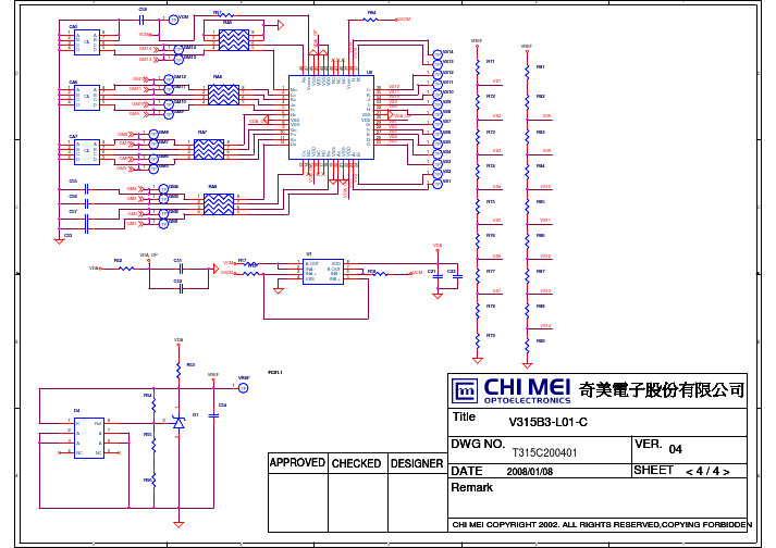
奇美V420H1-L15逻辑板原理图
笔记本维修思路及笔记本主板部分电路工作原理介绍

电脑维修军团本修品牌连锁维修军团原创图标示意为:小人携带维修包飞速的去抢救电脑,看起来还像一个“六”,寓意六六大顺笔记本维修思路及笔记本主板部分电路工作原理介绍一.显示屏故障:笔记本的显示屏看不到显示屏盖打开 屏背对着阳光 如果能看到东西 屏是好的 说明是灯管坏 不亮 或者屏坏灯管需要:400V-1000V 的供电 高压板对外150或200元 对内就30或50元屏线断了会出现白屏 屏线接触不良会出现屏一闪一闪出竖条等屏线分14针 20针 30针 如果14针屏线没有可以把20针屏线改为14针正常可用进水的笔记本会出现屏有不正常 可能是聚光板的问题二.笔记本主板:保护隔离电路是故障区:若损坏,插上适配器 装上电池 则自动隔离切断电池供电 开不了机系统供电电路出来3个电压3.3v 5v 12v 供给各个电路板供电电路系统供电芯片一般通常见到的是MAX1632芯片通常大部分都可以互换 外引脚两面腿 有的背光灯电路5v 供电是由系统供电电路供给系统供电单元电路常用芯片:A:MAX1632 MAX1635 MAX1631 MAX1634 MAX1904 LTC1628 MAX785w ww .87887.c n2010.06.19 电脑维修军团本修品牌连锁维修军团原创图标示意为:小人携带维修包飞速的去抢救电脑,看起来还像一个“六”,寓意六六大顺MAX786等键盘芯片 M38857 M38867 M38869 H8/3434 H8/3437 H8/2147 H8/2149 H8/2169 PC87570 PC87591等如果损坏开不了机等其他原因CPU 温度监控芯片 MAX1617 AD1030A AD1020A CM8500等如果损坏风扇一直转或不转等PC 卡芯片 PCIBUS R5C552 R5C476 R5C472等PC 卡供电芯片 TPS2205 TPS2206 TPS2216 TPS2211 TPV2211 M2563A M2564A作用:最早使用目的为扩展内存 现在可连接网卡 猫 光驱 软驱 硬盘 存储卡 CDMA 声卡 传真卡等声卡芯片:ESS19215 4299-JQ 4297A-JQ CS4239-KQ 等有的和台式机主板的声卡一样功放芯片:ESS19805 ACL8810 TPA0202 8552TS 854ZTS BA7786I/O 芯片: pc87371 pc87392 pc87393 pc97338 smsc fdc57n869 fdc37n958 lpc47n267 lpc47n227等串口芯片:MAX3243 AAX213 ADM213 HIN213 SP3243 MCI45583等 充电原理:当电池电压低于内部设定值时,MAX1645内部振荡开机起振工作 23和20脚有高低端脉冲信号输出入推动高低端管工作 16V 输出的充电电压通过L1储能电感R2精密取样电阻 为电池充电另一路经R11 R16组成的电流反馈电路检测到充电电流的大小 控制输出的充电电流稳定 随着电池电压的不断升高经数据线SDA 时钟SCL 把电池电压信息反馈到13 14脚去控制内部振荡电路的振荡工作频率最终控制外部高低端管子的导通时间的长短调整充电电流的大小 另一路SDA SCL 反馈到NQ 南桥到CPU 到BQ 到显卡到液晶屏显示充电状态给用户以提示当电池充满时 经反馈线让芯片内部振荡器停止工作整机充电完成电池是否充电由28脚比较电压输入与9脚BATT 电池电压输入在芯片内部比较后决定时钟电路检修1.时钟供电一般有2个电压供给3.3V2.5v 2.时钟芯片供电电感容易坏3.测14.318晶振两端是否有0.03左右的电压差 如晶振一段3.3另一端0V 也是此晶振坏了 4.如14.318两端电压为0V 可能时钟芯片坏或两脚对地稳频电容损坏5.如果晶振起振 测时钟芯片外围33欧 22欧小电阻是否正常 上面是否有时钟信号电压该w ww .87887.c n2010.06.19 电脑维修军团本修品牌连锁维修军团原创图标示意为:小人携带维修包飞速的去抢救电脑,看起来还像一个“六”,寓意六六大顺电压一般等于时钟电路供电的2分子1 (如供电为3.3V 那么时钟信号电压应为1.65v) 6.P4与迅驰CPU 时钟信号电压为0.4-0.9V笔记本的硬启动过程插上电源适配器使机器在待机状态 按下电源开关如果整机供电系统正常 那么供电芯片(MAX1632 MAX1711)PG 信号产生分别送到南桥 北桥 CPU 南桥接到PG 信号后 就会产生2路时钟控制芯片CPU-STOP PCI-STOP 送到时钟芯片 时钟芯片工作正常后 就会产生各路时钟信号 送到主板的各个电路 其中一路时钟送到南桥 南桥接到时钟信号后就会产生出2路复位信号 分别为PCI-BST DRV-RST 去复位主板上的各个电路 其中一路PCI RST 去复位北桥 当BQ 接到复位信号后 产生CPU RST 去复位CPU 当CPU 接到复位信号后表示硬启动完成。
逻辑板工作原理页PPT文档
液晶屏的基本构造及组成
• 液晶屏是由多层不同作用的薄片组成,有偏振片、配向膜、滤色 片、液晶层、背先板等,下图所示就是液晶屏的最主要组成的断 面示意图
• 液晶层在配向膜的中间,先线由下部背先灯射入, 穿后过偏振片、配向膜在液晶层叐到电信号控制 的液晶分子的控制再穿过配向膜及前偏振片,我 们看到的就是图像。
• 电路中,列驱动器(源极驱动器)的作用是,在 外部行同步脉冲的同步作用下,能够使TFT场效 应管的源极列线从左至右逐根逐条他加电,以使 每一行水平像素,自左至右他逐个燃亮,产生类 似电视的行扫描作用。行驱动器(栅极驱动器) 的作用是;在外部帧同步脉冲的同步下,将TFT 场效应管的栅极扫描线(水平方向)逐条加上电 压,控制TFT元件的导通与截止,以产生自上而 下的每行扫描,从而产生类似电视的场扫描。
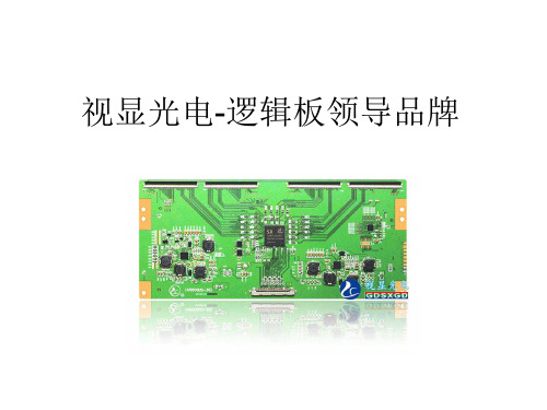
视显光电-逻辑板领导品牌
液晶显示屏的认识
LCD屏型号命名规则
• AU 台湾友达 L或M开头 M170E5-L05 E表示1280×1024分辨率 • X:1024×768 E:1280×1024 PW:1440×900 • BOE 京东方 H开头 H17E13-100 • CHIMEI/CMO 台湾奇美/奇丽 M/N M150XS-T0S • HANNSTAR 瀚彩 HSD150X82 • HITACHI 日立 TX/SX (真彩/伪彩) TX38D14 • SHARP 夏普 LQ LQ150X 3 • TORISAN 广辉(广达) QD • FUJITSU 富士通 EDTC/CA • HYUNDAI 现代 HT HT17E11-200 • LG-PHILIPS LQ/LP/LC/CA • TORISAN 三洋 TM TM190SX-70 SX表示SXGA • NEC 日电NL10276BC30 102表示1024, 76表示768 1024×768 • SAMSUNG 三星 LIM150XH-LO1
逻辑板维修 新
二、图像不良
① U1(CM2679B)损坏假焊(测LVDS信号输入 对地阻值一样,不一样一般为U1坏)
② VCOM5.5V供电丢失出现图像发白
③伽马电压较正芯片损坏出现图不良
④各供电出现偏低偏高出现图不良热机图不良无图 等
奇美V370H1-L0A逻辑板元件识别图
VDDC 3.3V
VDA 13.5V
LP4
UP3 MAX1858
9V
LP3
UP2 FPS138
12V输入 CP28,DP7,Q9等元件损坏造成无23V输出无图
主要故障:13.5V 23V滤波电容短路无电压输出无图
奇美V370H1-L0A
适用机型:LC-TM3719
,LC37BT19C, LC-TM4219, LC-TM4711等。
主要故障:
VGL- 5.6V
接U3 63脚 3.3V
当此处为3.3V时⑤脚输 出驱动信号后级产生各 组VDA VGH VGL等电压
故障元件引起故障现象及其判断方法:
一、U6(AS15-G) 损坏出现无图,图不良,可通过触摸芯片温度判 断,若损坏会严重发烫
二、U3(CM2681A)假焊或损坏出现无图/热机无图,图不良/热机图 不良等。若损坏可测N7 2.5V N6 3.3V对地阻值是否变小短路等。 (正常时为320欧左右)
V315B3-L04逻辑板元件识别图
VCM 3.3V VDA 13.5V
U3
U6
VGH 20V VGL-6.5V
VAAP 13.5V
QP2
HX8915-A
UP5UP6
1.8V
CM1682A
23脚LVDS数据格式选择 32脚PWRON高电平3.3V 时控制UP1⑨脚UP1与外 部升压电路产生各组供电
奇美32寸液晶屏电路原理图
GM12 A B C D 8 7 6 5 GM11 GM10 GM9
TP TP TP TP
1 1 1
GM11 GM10 GM9
1 2 3 4
8 7 6 5
VDA_OP GM8 A B C D 8 7 6 5 GM7 GM6 GM5 C55 GM4 C56
C
1 1 1 1
CA7 1 A 2 B CA 3 C 4 D
V315B3-L01-C
T315C200401
2008/01/08
VER. 04 SHEET <4/4>
A
A
R56
DATE Remark
CHI MEI COPYRIGHT 2002. ALL RIGHTS RESERVED,COPYING FORBIDDEN
5 4 3 2 1
5
4
3
2
1
CN2
CN1 XRP2 XRP1 GM14 GM13 GM12 GM11 GM10 GM9 GM8 GM7 GM6 GM5 GM4 GM3 GM2 GM1 VCM VDA VREF VDD
CM1682A-K1
POL STH_R STH GND VDD25 TP1 STV_R OE GND VDD18 VDD25 GND VDD25 GND VDD25 GND VDD25 GND VDD25 GND VDD25 GND GND VDD18 GRL1 CKV STV GVON GVOFF GND VDD25 PWRON
5
4
3
2
1
C58 1 CA5 1 A 2 B CA 3 C 4 D 8 7 6 5 TP VCM
R57 RA5 1 2 3 4 8 7 6 5 VDA_OP
笔记本主板电源原理及架构

笔记本主板电源原理及架构通常情况下,笔记本由适配器或电池供电。
常用适配器的典型输出电压为。
电池通常输出、等。
但主板内部各部分的工作电压并没有这么高。
如DDRIII内存工作电压通常为,LAN工作电压为,硬盘、MODEN 等需要5V等等。
除了工作电压不同以外,主板不同部分对电源的带负载能力要求也不同。
例如DDRII内存通常要求电源能提供8A左右的电流。
而CPU则往往需要超过30A以上且变化速率很高的电流。
针对不同要求,我们需要把适配器或电池提供的电,经过精确的变换之后,再分配给不同的部分。
设计笔记本主板电源部分的目的,简单的说,就是利用适配器或电池提供的电能,为主板各个部分单独制定合适的供电方案。
下图为一典型电源架构图。
图典型笔记本电源总架构由图可以看出,适配器或电源经过众多变换,最终分成很多不同的部分。
本文所有章节即围绕此图展开,详细的介绍各个部分的作用、特性以及解决方案。
上图为外部电源(适配器或电池)与主板电源相连接的部分,也是一个更加简略的架构图。
外部电源的电压会被分布到一个电源平面上,以某品牌商务机种架构为例,此平面称为+PWR_SRC。
若适配器和电池都在,电池处在充电状态或不工作,+PWR_SRC 电压即为适配器的电压,通常为。
若只有适配器接入,情况相同。
若只有电池接入,+PWR_SRC 为电池输出电压,通常为或。
主板各个部分不同的电源都直接或间接的由+P WR_SRC 转换得来。
图中使用了FDC654P 来将+PWR_SRC 转换成+BL_PWR_SRC,用ISL62870 将+PWR_SRC 转换为+GPU_CORE, +GPU_CORE 为显卡的工作电源。
除了电源变换外,从上图还可以看出,电池的充电电路也是电源架构的一部分。
详情将会在以后章节中具体分析。
主板维修技巧主板维修技巧及是否不良)3-1-3. 查BATTERY之SHORT PIN(JUMPER)是否未上或上錯位置BATTERY 之電壓是否正確,CRYSTAL頻率及其相關線路是否正常3-2﹒PCIRST不正確查CHIP之PCIRST至PCI SLOT(PIN A15)之線路是否OPEN or SHORT或零件不良3-3 CPURST不正確查CHIP至CPU之線路是否OPEN or SHORT或零件不良4. 查BE0~BE7,A2~A31,D0~D63等信號及其相關之線路是否OPEN or SHORT或零件不良5﹒查ADS,CPURDY,PCI之REQ0~REQ3,等信號及其相關之線路是否OPEN or SHORT或零件不良6﹒查PCI SLOT之AD0~AD31等信號及其相關之線路是否OPEN orSHORT或零件不良7﹒BIOS不良或無資料(可使用良品之BIOS交換測試確定之)8﹒查SA0~SA16,SD0~SD7(XD0~XD7)等信號及其相關之線路是否OPEN or SHORT或零件不良1.熟悉PC主板的总线类型及I/O总线插槽中各信号排列情况,以I/O插槽中重要信号为线索进行故障点查找是维修PC主板致命性故障的关键。
液晶电视逻辑板原理分析与检修
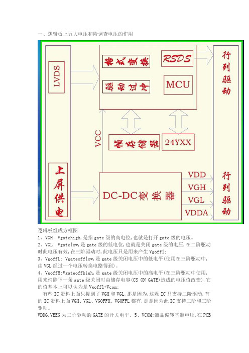
一、逻辑板上五大电压和阶调查电压的作用逻辑板组成方框图1、VGH: Vgatehigh,是指gate级的高电位,也就是打开gate级的电压。
2、VGL: Vgatelow,是gate级的低电位,也就是关闭gate级的电压,在二阶驱动时此电压有效,在三阶驱动时,此电压只是用来产生Vgoffl;3、VgoffL: Vgateofflow,是gate级关闭电压中的低电平(使用在三阶驱动中,由VGL经过一个电压转换电路得到)。
4、VgoffH:Vgateoffhigh,是gate级关闭电压中的高电平(在三阶驱动中使用,用来消除下一条gate级关闭时由储存电容(CS ON GATE)造成的电压值改变),它的值基本上可以认为是Vgoffl+Vcom;有些IC资料上面只提到了VGH和VGL,那是因为,这颗IC只支持二阶驱动,有的IC资料上面VGH、VGL、VGOFFH、VGOFFL都有,那是因为此IC支持二阶和三阶驱动。
VDDG,VEEG为二阶驱动的GATE的开关电平。
5、VCOM:液晶偏转基准电压;在PCB上VDDA会通过分压的回路分出10~14组电压,作为IC内部DAC时的输出VGMA 的基准电压,通过PCB的分压电路,产生多组参考电压,可以减少IC内部的分压电路。
SPP9435结构图TPS65161内部结构方框图二、VDDD是数字电路的工作电压;(SW) 5脚(SW)内部电路组成的升压电路开始工作,输出约16V的电压,UP1第27脚(GD)为QP1、QP2提供一个开启信号,16V电压经过QP1,QP2得到VDA电压为行列驱动电路提供供电.当以上电路都正常工作后,VAAP经过由DP5、CP18、UP1第10脚(DRP)内部组成的升压电路开始正常工作,通过RP21限流得到VGHP电压,VGHP通过QP8输出22V左右的VGH电压为行列驱动提供供电.从以上分析可以看出,该电路正常启动工作时存在严格的时序关系.因此依此时序关系分别检查各路电压,发现VGHP电压仅为10.5V,而正常时为19.5V.VGH电压为0V,正常时应为18V.显然问题是因VGHP电压不能正常升压引起的.经检测UP1的第10脚电压为0V,而正常时10脚应能检测到2.25V的直流电压,交流检测时有5V左右的交流电压,但实测交直流电压均检测不到,测量该脚对地电阻无异常,怀疑UP1第10脚内部损坏,更换后故障排除。
全面讲解电脑主板构造及原理(图解)

全面讲解电脑主板构造及原理(图解)(一)2007-09-04 20:44全面讲解电脑主板构造及原理(图解)(一)2007-09-04 20:44虽然此文较老,但不失为一骗不可多得的经典帖。
希望能对大家有帮助。
大家知道,主板是所有电脑配件的总平台,其重要性不言而喻。
而下面我们就以图解的形式带你来全面了解主板。
一、主板图解 一块主板主要由线路板和它上面的各种元器件组成1.线路板PCB印制电路板是所有电脑板卡所不可或缺的东东。
它实际是由几层树脂材料粘合在一起的,内部采用铜箔走线。
一般的PCB线路板分有四层,最上和最下的两层是信号层,中间两层是接地层和电源层,将接地和电源层放在中间,这样便可容易地对信号线作出修正。
而一些要求较高的主板的线路板可达到6-8层或更多。
主板(线路板)是如何制造出来的呢?PCB的制造过程由玻璃环氧树脂(GlassEpoxy)或类似材质制成的PCB“基板”开始。
制作的第一步是光绘出零件间联机的布线,其方法是采用负片转印(Subtractivetransfer)的方式将设计好的PCB线路板的线路底片“印刷”在金属导体上。
这项技巧是将整个表面铺上一层薄薄的铜箔,并且把多余的部份给消除。
而如果制作的是双面板,那么PCB的基板两面都会铺上铜箔。
而要做多层板可将做好的两块双面板用特制的粘合剂“压合”起来就行了。
接下来,便可在PCB板上进行接插元器件所需的钻孔与电镀了。
在根据钻孔需求由机器设备钻孔之后,孔璧里头必须经过电镀(镀通孔技术,Plated-Through-Holetechnology,PTH)。
在孔璧内部作金属处理后,可以让内部的各层线路能够彼此连接。
在开始电镀之前,必须先清掉孔内的杂物。
这是因为树脂环氧物在加热后会产生一些化学变化,而它会覆盖住内部PCB层,所以要先清掉。
清除与电镀动作都会在化学过程中完成。
接下来,需要将阻焊漆(阻焊油墨)覆盖在最外层的布线上,这样一来布线就不会接触到电镀部份了。
V420H1-L15_Approval_Spec_Ver2_090223

TFT LCD Approval SpecificationMODEL NO.: V420H1 – L15TV Head DivisionApproved ByLY ChenQA Dept. Product Development Div.Reviewed ByKc_KoWT LinLCD TV Marketing and Product Management Div.Prepared ByWang-Yang Li Sisley WuCONTENTSREVISION HISTORY (4)1. GENERAL DESCRIPTION (5)1.1 OVERVIEW (5)1.2 FEATURES (5)1.3 APPLICATION (5)1.4 GENERAL SPECIFICATIONS (5)1.5 MECHANICAL SPECIFICATIONS (6)2. ABSOLUTE MAXIMUM RATINGS (7)2.1 ABSOLUTE RATINGS OF ENVIRONMENT (7)2.2 PACKAGE STORAGE (8)2.3 ELECTRICAL ABSOLUTE RATINGS (8)2.3.1 TFT LCD MODULE (8)2.3.2 BACKLIGHT INVERTER UNIT (8)3. ELECTRICAL CHARACTERISTICS (9)3.1 TFT LCD MODULE (9)3.2 BACKLIGHT CONNECTOR PIN CONFIGURATION (11)3.2.1 LAMP SPECIFICATION (11)3.2.2 ELECTRICAL SPECIFICATION (11)3.2.3 INVERTER INTERFACE CHARACTERISTICS (13)4. BLOCK DIAGRAM OF INTERFACE (15)4.1 TFT LCD MODULE (15)5. INPUT TERMINAL PIN ASSIGNMENT (16)5.1 TFT LCD Module Input (16)5.2 BACKLIGHT UNIT (18)5.3 INVERTER UNIT (18)5.4 BLOCK DIAGRAM OF INTERFACE (18)5.5 LVDS INTERFACE (22)5.6 COLOR DATA INPUT ASSIGNMENT (23)6. INTERFACE TIMING (24)6.1 INPUT SIGNAL TIMING SPECIFICATIONS (24)6.2 POWER ON/OFF SEQUENCE (26)7. OPTICAL CHARACTERISTICS (27)7.1 TEST CONDITIONS (27)7.2 OPTICAL SPECIFICATIONS (28)8. PRECAUTIONS (31)8.1 ASSEMBLY AND HANDLING PRECAUTIONS (31)8.2 SAFETY PRECAUTIONS (31)9. DEFINITION OF LABELS (32)9.1 CMO MODULE LABEL (32)10. PACKAGING (33)10.1 PACKAGING SPECIFICATIONS (33)10.2 PACKAGING METHOD (33)11. MECHANICAL CHARACTERISTICS (36)REVISION HISTORYVersion Date Page(New) Section DescriptionVer. 0.0 Nov. 06, 2008 All All The tentative specification was first issued. Ver. 1.0Dec. 19, 2008 9 11 11-12 1318 22-23 26 28 33 3.13.2.1 3.2.23.2.3 5.3 5.5 6.2 7.2 10.2Updated TFT LCD Module Parameter Updated Lamp SpecificationUpdated BL Electrical Specification Updated Internal PWN Control Voltage Updated Pin 12 define Updated LVDS InterfaceUpdated Power ON/OFF Sequence Updated Optical SpecificationsUpdated Figure.10-1 packing method Ver. 1.0 Dec. 23, 2008 18 5.3 Updated inverter pin 12 define Ver. 1.1 Dec. 31, 2008 13 3.2.3 add note(4)14 3.2.3 Updated power sequence and control signal timing fig. Ver. 2.0Feb. 16. 2009 9 11 16 21 24 27 28~30 33~34 36~38 3.13.2.1 5.5.1 5.4 6.6.1 7.1 7.2 10.1 11Update Power Supply CurrentUpdate Lamp Specification & Electrical specification Update Input Terminal Pin Assignment Update Block Diagram of Interface note 3 Input Signal Timing Specifications update Updated optical measurement condition Optical Specifications updateUpdate Mechanical Characteristics Update Packaging specifications1. GENERAL DESCRIPTION1.1 OVERVIEWV420H1-L15 is a 42” TFT Liquid Crystal Display module with 12-CCFL Backlight unit and 2ch-LVDS interface.This module supports 1920 x 1080 Full HDTV format and can display 16.7M colors (8-bit/color). The inverter module for backlight is built-in.1.2 FEATURESЁHigh brightness (500 nits)ЁHigh contrast ratio (4000:1)ЁFast response time (Gray to gray average 6.5 ms)ЁHigh color saturation (NTSC 72%)ЁFull HDTV (1920 x 1080 pixels) resolution, true HDTV formatЁDE (Data Enable) only modeЁLVDS (Low Voltage Differential Signaling) interfaceЁOptimized response time for 60 Hz frame rateЁUltra wide viewing angle : Super MVA technologyЁRoHS compliance1.3 APPLICATIONЁStandard Living Room TVs.ЁPublic Display Application.ЁHome Theater Application.ЁMFM Application.1.4 GENERAL SPECIFICATIONSItem Specification Unit Note Active Area 930.24(H) x 523.26 (V) (42.02” diagonal) mm(1)Bezel Opening Area 937.24 (H) x 530.26 (V) mmDriver Element a-si TFT active matrix - -Pixel Number 1920 x R.G.B. x 1080 pixel -Pixel Pitch(Sub Pixel) 0.1615 (H) x 0.4845 (V) mm -Pixel Arrangement RGB vertical stripe - -Display Colors 16.7M color -Display Operation Mode Transmissive mode / Normally black - -Surface Treatment Anti-Glare coating (Haze 11%) - (2)Note (1) Please refer to the attached drawings in chapter 9 for more information about the front and back outlines.Note (2) The spec. of the surface treatment is temporarily for this phase. CMO reserves the rights to change this feature.1.5 MECHANICAL SPECIFICATIONSItem Min. Typ. Max. Unit NoteHorizontal (H) - 983.0 - mm(1), (2)Module SizeVertical (V) - 576.0 - mmDepth (D) - 50.8 - mm Weight - (10400) - g - Note (1) Please refer to the attached drawings for more information of front and back outline dimensions.Note (2) Module Depth is between bezel to T-CON cover.2. ABSOLUTE MAXIMUM RATINGS2.1 ABSOLUTE RATINGS OF ENVIRONMENTValueUnit NoteItem SymbolMin. Max.Storage Temperature TST -20 +60 ºC (1)Operating Ambient Temperature TOP 0 50 ºC (1), (2)Shock (Non-Operating) SNOP - 50 G (3), (5)Vibration (Non-Operating) VNOP - 1.0 G (4), (5) Note (1) Temperature and relative humidity range is shown in the figure below.(a) 90 %RH Max. (Ta Љ40 ºC).(b) Wet-bulb temperature should be 39 ºC Max. (Ta > 40 ºC).(c) No condensation.Note (2) The maximum operating temperature is based on the test condition that the surface temperature of display area is less than or equal to 65 ºC with LCD module alone in a temperature controlled chamber.Thermal management should be considered in final product design to prevent the surface temperature ofdisplay area from being over 65 ºC. The range of operating temperature may degrade in case ofimproper thermal management in final product design.Note (3) 11 ms, half sine wave, 1 time for ± X, ± Y, ± Z.Note (4) 10 ~ 200 Hz, 10 min, 1 time each X, Y, Z.Note (5) At testing Vibration and Shock, the fixture in holding the module has to be hard and rigid enough so that the module would not be twisted or bent by the fixture.2.2 PACKAGE STORAGEWhen storing modules as spares for a long time, the following precaution is necessary.(a) Do not leave the module in high temperature, and high humidity for a long time, It is highly recommended tostore the module with temperature from 0 to 35 кat normal humidity without condensation.(b) The module shall be stroed in dark place. Do not store the TFT-LCD module in direct sunlight or fluorescentlight.2.3 ELECTRICAL ABSOLUTE RATINGS2.3.1 TFT LCD MODULEValueUnit Note Item SymbolMin. Max.Power Supply Voltage VCC -0.3 13.5 V(1)Logic Input Voltage VIN -0.3 3.6 V2.3.2 BACKLIGHT INVERTER UNITValueUnit Note Item SymbolMin. Max.Lamp Voltage VW Ё3000 VRMSPower Supply Voltage VBL 0 30 V (1)Control Signal Level Ё-0.3 7 V (1), (3)Note (1) Permanent damage to the device may occur if maximum values are exceeded. Function operation should be restricted to the conditions described under Normal Operating Conditions.Note (2) No moisture condensation or freezing.Note (3) The control signals include On/Off Control and Internal PWM Control.3. ELECTRICAL CHARACTERISTICS3.1 TFT LCD MODULE(Ta = 25 ± 2 ºC)Value ParameterSymbolMin.Typ. Max. UnitNotePower Supply VoltageVCC 10.81213.2 V(1) Rush CurrentI RUSH - - 4.3 A (2)White Pattern- - 0.84 1.1 A Vertical Stripe - - 0.83 - A Power Supply CurrentBlack Pattern- - 0.48 - A (3) Common Input Voltage V LVC 1.125 1.25 1.375 V LVDS interface Terminating Resistor R T - 100 - ohm Input High Threshold Voltage V IH 2.7 - 3.3 V CMOS interface Input Low Threshold VoltageV IL-0.7VNote (1) The module should be always operated within the above ranges. Note (2) Measurement condition:Vcc rising time is 470usNote (3) The specified power supply current is under the conditions at Vcc = 12 V, Ta = 25 ± 2 ºC, f v = 60 Hz,whereas a power dissipation check pattern below is displayed.Active Areac. V ertical Stripe PatternActive AreaActive Areaa. White Patternb. Black Pattern3.2 BACKLIGHT CONNECTOR PIN CONFIGURATION 3.2.1 LAMP SPECIFICATION(Ta = 25 ± 2 ºC)ValueParameterSymbol Min. Typ. Max. Unit Note Lamp Input Voltage VL - (1090) - Lamp Input Voltage VL Lamp Current IL 9.7 (10.2) 10.7 Lamp Current IL - - (1910) Lamp Turn On Voltage VS Lamp Turn On Voltage VS - - (1560)Operating Frequency FL 35 - 70 Operating Frequency FL Lamp Life Time LBL50,000--Lamp Life TimeLBL3.2.2 ELECTRICAL SPECIFICA TION(Ta = 25 ± 2 ºC)ValueParameterSymbolMin. Typ. Max. UnitNote- 130 - (5), IL = 10.2 mA Power Consumption P BL - 110 - W (5), IL = 8.7 mA Power Supply Voltage V BL 22.8 24.0 25.2 VDC- 5.4 - Power Supply Current I BL 4.6 ANon DimmingInput Ripple Noise - - - 912 mVP-P VBL=22.8V Oscillating Frequency F W 39.5 42.5 45.5 kHz Dimming Frequency F B 150 160 170 Hz Minimum Duty RatioD MIN1020-%(6)Note (1) Lamp current is measured by utilizing AC current probe and its value is average by measuring masterand slave board. VIPWM : 3V is 100%,V ADIM = HI : Lamp current is 10.2mA; V ADIM = LO : Lamp current is 8.7mA.Note (2) The lamp starting voltage V S should be applied to the lamp for more than 1 second after startup.Otherwise the lamp may not be turned on.Note (3) The lamp frequency may produce interference with horizontal synchronous frequency of the display inputsignals, and it may result in line flow on the display. In order to avoid interference, the lamp frequencyshould be detached from the horizontal synchronous frequency and itó harmonics as far as possible. Note (4) The life time of a lamp is defined as when the brightness is larger than 50% of its original value and the effective discharge length is longer than 80% of its original length (Effective discharge length is defined as an area that has equal to or more than 70% brightness compared to the brightness at the center point of lamp.) as the time in which it continues to operate under the condition at Ta = 25 ±2кand IL =9.7~10.7 mArms..Note (5) The measurement condition of Max. value is based on 42” backlight unit under input voltage 24V, average lamp current 10.2 mA and 8.7 mA ,lighting 30 minutes later.Note (6) 10% minimum duty ratio is only valid for electrical operation.3.2.3 INVERTER INTERFACE CHARACTERISTICSValueParameterSymbolTestConditionMin. Typ.Max. Unit NoteON Ё 2.0 Ё 5.0 V On/Off Control Voltage OFF V BLON Ё 0 Ё 0.8 VMAX Ё3.15Ё5.0V Max. Duty Ratio Internal PWM Control VoltageMIN V IPWMЁ Ё0 ЁV Min. Duty RatioHI Ё 3.0 3.33.6 V Normal Status Signal LOStatus Ё 0 Ё 0.8V AbnormalVBL Rising Time Tr1 Ё 30 Ё Ё ms VBL Falling TimeTf1 Ё 30Ё Ёms See as belowControl Signal Rising Time Tr Ё Ё Ё 100 ms Control Signal Falling Time Tf Ё Ё Ё 100 ms PWM Signal Rising Time T PWMR Ё Ё Ё 50 us PWM Signal Falling Time T PWMF Ё ЁЁ 50usInput Impedance R IN Ё 1 Ё Ё M Ω PWM Delay Time T PWM Ё 100 Ё Ё ms BLON Delay Time T onЁ 300 Ё Ё ms BLON Off TimeT on1Ё300ЁЁmsNote (1) The dimming signal should be valid before backlight turns on by BLON signal. It is inhibited tochange the internal/external PWM signal during backlight turn on period.Note (2) The power sequence and control signal timing are shown in the following figure. For a certainreason, the inverter has a possibility to be damaged with wrong power sequence and control signal timing.Note (3) While system is turned ON or OFF, the power sequences must follow as below descriptions: Turn ON sequence: VBL Ш PWM signal Ш BLONTurn OFF sequence: BLOFF Ш PWM signal Ш VBLNote (4) When the Dynamic CR has been turned on, the skipped range of VIPWM, 2.85V ~ 3.15V, issuggested to avoid the abnormal phenomenon.4. BLOCK DIAGRAM OF INTERFACE 4.1 TFT LCD MODULE5. INPUT TERMINAL PIN ASSIGNMENT5.1 TFT LCD Module InputPin Name Description Note1 GND Ground2 N.C. No Connection3 N.C. No Connection4 N.C. No Connection5 N.C. No Connection6 N.C. No Connection (1)7 SELLVDS LVDS data format Selection (2)8 N.C. No Connection (1)9 ODSEL Overdrive Lookup Table Selection(3)10 N.C. No Connection (1)11 EN_DCR Enable Dynamic Backlight (4)12 ERX0- Even pixel Negative LVDS differential data input. Channel 013 ERX0+ Even pixel Positive LVDS differential data input. Channel 014 ERX1- Even pixel Negative LVDS differential data input. Channel 115 ERX1+ Even pixel Positive LVDS differential data input. Channel 116 ERX2- Even pixel Negative LVDS differential data input. Channel 217 ERX2+ Even pixel Positive LVDS differential data input. Channel 218 GND Ground19 ECLK- Even pixel Negative LVDS differential clock input20 ECLK+ Even pixel Positive LVDS differential clock input21 GND Ground22 ERX3- Even pixel Negative LVDS differential data input. Channel 323 ERX3+ Even pixel Positive LVDS differential data input. Channel 324 N.C. No Connection25 N.C. No Connection26 N.C. No Connection (1)27 N.C. No Connection (1)28 ORX0- Odd pixel Negative LVDS differential data input. Channel 029 ORX0+ Odd pixel Positive LVDS differential data input. Channel 030 ORX1- Odd pixel Negative LVDS differential data input. Channel 131 ORX1+ Odd pixel Positive LVDS differential data input. Channel 132 ORX2- Odd pixel Negative LVDS differential data input. Channel 233 ORX2+ Odd pixel Positive LVDS differential data input. Channel 234 GND Ground35 OCLK- Odd pixel Negative LVDS differential clock input.36 OCLK+ Odd pixel Positive LVDS differential clock input.37 GND Ground38 ORX3- Odd pixel Negative LVDS differential data input. Channel 339 ORX3+ Odd pixel Positive LVDS differential data input. Channel 340 N.C. No Connection41 N.C. No Connection42 N.C. No Connection (1)43 N.C. No Connection (1)44 GND Ground45 GND Ground46 GND Ground47 GND Ground48 VCC +12V power supply49 VCC +12V power supply50 VCC +12V power supply51 VCC +12V power supplyNote (1) Reserved for internal use. Please leave it open.Note (2)Low : VESA LVDS Format (default), High : JEIDA Format.Note (3) Overdrive lookup table selection. The overdrive lookup table should be selected in accordance with the frame rate to optimize image quality.ODSEL NoteL Lookup table was optimized for 60 Hz frame rate.H Lookup table was optimized for 50 Hz frame rate.Note ( 4) Low=Open or Connect to GND, High = Connect to +3.3V5.2 BACKLIGHT UNITThe pin configuration for the housing and the leader wire is shown in the table below.Pin Name Description Wire Color 1 HV High Voltage White 2HVHigh VoltagePink5.3 INVERTER UNITCN1: S14B-PH-SM4-TB(D)(LF)(JST) or equivalentPin № Symbol Feature 1 234 5VBL +24V6789 10GND GND 11 STATUSNormal (3.3V)Abnormal(GND)12 A_DIM Amplitude Dimming ControlHI (2.0V ~ 5.0V)LO(0V~0.8V)13 I_PWM Internal PWM Control Signal 14 BLON BL ON/OFF CN2-CN7: SM02 -BDAS-3-TB(JST) or equivalent Pin No. Symbol Description1 CCFL HOT CCFL high voltage2 CCFL HOT CCFL high voltageHV(White)HV(White) HV(White)CN8: 528520870 (Molex) or equivalent Pin No. Symbol Description1 Board to Board2 Board to Board3 Board to Board4 Board to Board5 Board to Board6 Board to Board7 Board to Board 8Control SignalBoard to BoardNote (1) Floating of any control signal is not allowed.5.4 BLOCK DIAGRAM OF INTERFACEER0-ER7 EG0-EG7 EB0-EB7DEHost Graphics Controller TxINPLL PLLER0-ER7EG0-EG7EB0-EB7DETimingControllerERx0+ERx0-ERx1+ERx1-ERx2+ERx2-ECLK+ECLK-RxOUT51Ө51Ө51Ө51Ө51Ө51Ө51Ө51Ө51Ө51Ө100pF100pF100pF100pF100pFERx3-ERx3+PLL PLLLVDS Transmitter THC63LVDM83A (LVDF83A)LVDS Receiver ORx0+ORx0-ORx1+ORx1-ORx2+ORx2-OCLK+OCLK-51Ө51Ө51Ө51Ө51Ө51Ө51Ө51Ө51Ө100pF100pF100pF100pF100pFORx3-ORx3+OR0-OR7 OG0-OG7 OB0-OB7DCLK OR0-OR7 OG0-OG7 OB0-OB7 DCLKER0~ER7: Even pixel R dataEG0~EG7: Even pixel G dataEB0~EB7: Even pixel B dataOR0~OR7: Odd pixel R dataOG0~OG7: Odd pixel G dataOB0~OB7: Odd pixel B dataDE: Data enable signalDCLK: Data clock signalNotes (1) The system must have the transmitter to drive the module.Notes (2) LVDS cable impedance shall be 50 ohms per signal line or about 100 ohms per twist-pair line when it is used differentially.Notes (3)Two pixel data send into the module for every clock cycle. The first pixel of the frame is even pixel and the second pixel is odd pixel.5.5 LVDS INTERFACEVESA LVDS forma ̇ΚʻRXCLK ̈́JEDIA LVDS forma ̇ΚʻRXCLK ̈́G3R2G5G4G6R7G2R6R5R4R3B2G7B3B4B6B5B7VS HS DE R0G0R1G1B1B0RSVDERX0̈́ERX1̈́ERX3̈́ERX2̈́R0~R7: Pixel R Data (7; MSB, 0; LSB) G0~G7: Pixel G Data (7; MSB, 0; LSB) B0~B7: Pixel B Data (7; MSB, 0; LSB) DE : Data enable signal DCLK : Data clock signalNotes: (1) RSVD (reserved) pins on the transmitter shall be “H” or “L”.5.6 COLOR DATA INPUT ASSIGNMENTThe brightness of each primary color (red, green and blue) is based on the 10-bit gray scale data input for the color. The higher the binary input, the brighter the color. The table below provides the assignment of the color versus data input.Data SignalRedGreen Blue ColorR7 R6 R5 R4 R3 R2 R1 R0 G7 G6 G5 G4 G3 G2 G1 G0 B7 B6 B5 B4 B3 B2 B1 B0Basic Colors Black Red GreenBlue CyanMagenta Yellow White0 1 0 0 0 1 1 1 0 1 0 0 0 1 1 1 0 1 0 0 0 1 1 1 0 1 0 0 0 1 1 1 0 1 0 0 0 1 1 1 0 1 0 0 0 1 1 1 0 1 0 0 0 1 1 1 0 1 0 0 0 1 1 1 0 0 1 0 1 0 1 1 0 0 1 0 1 0 1 1 0 0 1 0 1 0 1 1 0 0 1 0 1 0 1 1 0 0 1 0 1 0 1 1 0 0 1 0 1 0 1 1 0 0 1 0 1 0 1 1 0 0 1 0 1 0 1 1 0 0 0 1 1 1 0 1 0 0 0 1 1 1 0 1 0 0 0 1 1 1 0 1 0 0 0 1 1 1 0 1 0 0 0 1 1 1 0 1 0 0 0 1 1 1 0 1 0 0 0 1 1 1 0 1 0 0 0 1 1 1 0 1GrayScaleOfRedRed (0) / Dark Red (1)Red (2)::Red (253)Red (254) Red (255)0 0 0 : : 1 1 1 0 0 0 : : 1 1 1 0 0 0 : : 1 1 1 0 0 0 : : 1 1 1 0 0 0 : : 1 1 1 0 0 0 : : 1 1 1 0 0 1 : : 0 1 1 0 1 0 : : 1 0 1 0 0 0 : : 0 0 0 0 0 0 : : 0 0 0 0 0 0 : : 0 0 0 0 0 0 : : 0 0 0 0 0 0 : : 0 0 0 0 0 0 : : 0 0 0 0 0 0 : : 0 0 0 0 0 0 : : 0 0 0 0 0 0 : : 0 0 0 0 0 0 : : 0 0 0 0 0 0 : : 0 0 0 0 0 0 : : 0 0 0 0 0 0 : : 0 0 0 0 0 0 : : 0 0 0 0 0 0 : : 0 0 0 0 0 0 : : 0 0 0GrayScaleOfGreenGreen (0) / Dark Green (1)Green (2)::Green (253)Green (254) Green (255) 0 0 0 : : 0 0 0 0 0 0 : : 0 0 0 0 0 0 : : 0 0 0 0 0 0 : : 0 0 0 0 0 0 : : 0 0 0 0 0 0 : : 0 0 0 0 0 0 : : 0 0 0 0 0 0 : : 0 0 0 0 0 0 : : 1 1 1 0 0 0 : : 1 1 1 0 0 0 : : 1 1 1 0 0 0 : : 1 1 1 0 0 0 : : 1 1 1 0 0 0 : : 1 1 1 0 0 1 : : 0 1 1 0 1 0 : : 1 0 1 0 0 0 : : 0 0 0 0 0 0 : : 0 0 0 0 0 0 : : 0 0 0 0 0 0 : : 0 0 0 0 0 0 : : 0 0 0 0 0 0 : : 0 0 0 0 0 0 : : 0 0 0 0 0 0 : : 0 0 0GrayScaleOfBlueBlue (0) / Dark Blue (1)Blue (2)::Blue (253)Blue (254) Blue (255) 0 0 0 : : 0 0 00 0 0 : : 0 0 00 0 0 : : 0 0 00 0 0 : : 0 0 0 0 0 0 : : 0 0 0 0 0 0 : : 0 0 0 0 0 0 : : 0 0 0 0 0 0 : : 0 0 0 0 0 0 : : 0 0 0 0 0 0 : : 0 0 0 0 0 0 : : 0 0 0 0 0 0 : : 0 0 00 0 0 : : 0 0 00 0 0 : : 0 0 0 0 0 0 : : 0 0 0 0 0 0 : : 0 0 0 0 0 0 : : 1 1 1 0 0 0 : : 1 1 1 0 0 0 : : 1 1 1 0 0 0 : : 1 1 10 0 0 : : 1 1 1 0 0 0 : : 1 1 1 0 0 1 : : 0 1 1 0 1 0 : : 1 0 1Note (1) 0: Low Level Voltage, 1: High Level Voltage6. INTERFACE TIMING6.1 INPUT SIGNAL TIMING SPECIFICATIONS(Ta = 25 ± 2 ºC)The input signal timing specifications are shown as the following table and timing diagram.SignalItemSymbol Min. Typ. Max. Unit Note Frequency1/Tc 60 74.25 80 MHz - LVDS Receiver Clock Input cycle tocycle jitter Trcl - - 200 ps - Setup Time Tlvsu 600 - - ps - LVDS Receiver DataHold Time Tlvhd 600 - - ps - Fr5 47 50 53 Hz (1) Frame RateFr6 57 60 63 Hz (1)Total Tv 1115 1125 1135 Th Tv=Tvd+TvbDisplay Tvd 1080 1080 1080 Th - VerticalActive Display TermBlankTvb 35 45 55 Th -Total Th 1050 1100 1150 Tc Th=Thd+ThbDisplay Thd 960 960 960 Tc - Horizontal Active Display TermBlankThb90140190Tc-Note (1) : (ODSEL) = (H) , (L). Please refer to 5.1 for detail informationNote (2) : Since the module is operated in DE only mode, Hsync and Vsync input signals should be set to lowlogic level. Otherwise, this module would operate abnormally.6.2 POWER ON/OFF SEQUENCE(Ta = 25 ± 2 ºC)To prevent a latch-up or DC operation of LCD module, the power on/off sequence should be as the diagram below.Power ON/OFF SequenceNote (1) The supply voltage of the external system for the module input should follow the definition of Vcc.Note (2) Apply the lamp voltage within the LCD operation range. When the backlight turns on before the LCD operation or the LCD turns off before the backlight turns off, the display may momentarily becomeabnormal screen.Note (3) In case of Vcc is in off level, please keep the level of input signals on the low or high impedance. If T2<0,that maybe cause electrical overstress failure.Note (4) T4 should be measured after the module has been fully discharged between power off and on period.Note (5) Interface signal shall not be kept at high impedance when the power is on.7. OPTICAL CHARACTERISTICS7.1 TEST CONDITIONSItem Symbol Value Unit Ambient Temperature Ta 25±2 oCAmbient Humidity Ha 50±10 %RHSupply Voltage VCC 12 VInput Signal According to typical value in "3. ELECTRICAL CHARACTERISTICS"Lamp Current IL 8.7/10.2 mAOscillating Frequency (Inverter) FW 10.2 KHzVertical Frame Rate Fr 120 HzThe LCD module should be stabilized at given temperature for 1 hour to avoid abrupt temperature change during measuring. In order to stabilize the luminance, the measurement (CS-1000 or CA-210 calibrated by CS-1000) should be executed after lighting backlight for 1 hour in a windless room.7.2 OPTICAL SPECIFICATIONSThe relative measurement methods of optical characteristics are shown in 7.2. The following items should be measured under the test conditions described in 7.1 and stable environment shown in 7.1.ItemSymbol ConditionMin.Typ.Max. Unit Note Contrast Ratio CR (3000) (4000) - - Note (2) Response TimeGray togray - (6.5) (12) msNote (3) Noraml mode LC (400) (500) - cd/m 2 Note (4) Center Luminance ofWhiteECO mode LC (350) (450) - cd/m 2 Note (4), (7) White Variation δW - - (1.3) - Note (6) Cross TalkCT -- (4)% Note (5)Rx (0.652) - RedRy (0.333) - Gx (0.270)-GreenGy (0.617) - Bx (0.149) - BlueBy (0.063) - Wx (0.280) - White Wy Typ. -0.03(0.285) Typ. +0.03--ColorChromaticityColor Gamut C.G θx=0°, θy =0° Viewing angle at normal direction- (72) - % NTSCθx+ 80 88 - Horizontalθx- 80 88 - θY+ 80 88 - Viewing AngleVerticalθY- CR ≥2080 88 - Deg. Note (1)Gamma-(2.2)-- -Note (1) Definition of Viewing Angle (θx, θy):Viewing angles are measured by Eldim EZ-Contrast 160RThe driving signal means the signal of gray level 0, 31, 63, 95, 127, 159, 191, 223 and 255.Gray to gray average time means the average switching time of gray level 0, 31, 63, 95, 127, 159, 191, 223 and 255 to each other.Note (4) Definition of Luminance of White (L C , L AVE ):Measure the luminance of gray level 255 at center point and 5 pointsL C = L (5), where L (X) is corresponding to the luminance of the point X at the figure in Note (6).Note (5) Definition of Cross Talk (CT):CT = | YB – YA | / YA × 100 (%)Where:YA = Luminance of measured location without gray level 0 pattern (cd/m2)YB = Luminance of measured location with gray level 0 pattern (cd/m2)8. PRECAUTIONS8.1 ASSEMBLY AND HANDLING PRECAUTIONS[ 1 ] Do not apply rough force such as bending or twisting to the module during assembly.[ 2 ] It is recommended to assemble or to install a module into the user’s system in clean working areas. The dust and oil may cause electrical short or worsen the polarizer.[ 3 ] Do not apply pressure or impulse to the module to prevent the damage of LCD panel and Backlight.[ 4 ] Always follow the correct power-on sequence when the LCD module is turned on. This can prevent the damage and latch-up of the CMOS LSI chips.[ 5 ] Do not plug in or pull out the I/F connector while the module is in operation.[ 6 ] Do not disassemble the module.[ 7 ] Use a soft dry cloth without chemicals for cleaning, because the surface of polarizer is very soft and easily scratched.[ 8 ] Moisture can easily penetrate into LCD module and may cause the damage during operation.[ 9 ] When storing modules as spares for a long time, the following precaution is necessary.[ 9.1 ] Do not leave the module in high temperature, and high humidity for a long time. It is highly recommended to store the module with temperature from 0 to 35кat normal humidity withoutcondensation.[ 9.2 ] The module shall be stored in dark place. Do not store the TFT-LCD module in direct sunlight or fluorescent light.[ 10 ] When ambient temperature is lower than 10ºC, the display quality might be reduced. For example, the response time will become slow, and the starting voltage of CCFL will be higher than that of roomtemperature.8.2 SAFETY PRECAUTIONS[ 1 ] The startup voltage of a Backlight is approximately 1000 Volts. It may cause an electrical shock while assembling with the inverter. Do not disassemble the module or insert anything into the Backlight unit.[ 2 ] If the liquid crystal material leaks from the panel, it should be kept away from the eyes or mouth. In case of contact with hands, skin or clothes, it has to be washed away thoroughly with soap.[ 3 ] After the module’s end of life, it is not harmful in case of normal operation and storage.V420H1 -L15Rev. XXX X X X X X X Y M D L N N N NV420H1 -L15Rev. XXX X X X X X X Y M D L N N N NModel Name: V420H1-L15Revision: Rev. XX, for example: A0, A1… B1, B2… or C1, C2…etc. Serial ID: X X X X X X X Y M D L N N N NSerial No.Product LineManufactured Date:Year: 0~9, for 2000~2009Month: 1~9, A~C, for Jan. ~ Dec.Day: 1~9, A~Y, for 1st to 31st, exclude I ,O, and U. Revision Code: Cover all the changeSerial No.: Manufacturing sequence of productProduct Line: 1 -> Line1, 2 -> Line 2, …etc.10. PACKAGING10.1 PACKAGING SPECIFICATIONS(1) 4 LCD TV modules / 1 Box(2) Box dimensions : 1100(L)x317(W)x670(H)mm(3) Weight : Approx. 53.17Kg(4 modules per carton)10.2 PACKAGING METHODFigures 10-1 and 10-2 are the packing methodFigure.10-1 packing methodSea / Land Transportation(40ft Container)Air TransportationFigure.10-2 packing method11. MECHANICAL CHARACTERISTICS。