基于DA14580智能蓝牙控制器开发多功能遥控器
DA14580最小蓝牙模块

DA14580最小蓝牙模块MN581A 模块是针对无线智能产品设计的一款超低功耗的,超小体积的蓝牙模块。
基于德国DAILOG超级蓝牙芯片DA14580设计,包含天线部分仅有5.50mm*8.0mm,高度仅有1.7mm 片上集成32 位ARM Cortex M0™处理器国际标准的Blue-tooth® Smart协议栈。
特别适合对体积和高度有特殊需求的智能穿戴式设备。
例如智能手环,蓝牙手表、无线键盘、无线鼠标、平板电脑、手机、笔记本电脑等产品。
可帮助客户快速开发蓝牙4.0产品。
1.1 主要的特点超低功耗最小尺寸内嵌16MHZ32位ARMCortexM0™处理器专用链路层处理器内置aes-128位加密处理器-Time-Programmable(OTP)内存系统SRAM记忆存储器支持多个数字接口:通用I/o、2个UARTs与硬件流控制1MBd、SPI+™接口总线在100kHz,400千赫硬件正交解码能力支持模拟接口设备内置4通道10-bitADC完全集成2.4GHzCMOS收发器单线天线:内置50欧姆天线匹配直接连接2.4G的天线电源电流:传输输出功率-93dBm接收机灵敏度1.2 应用市场智能穿戴式设备蓝牙手表无线键盘无线鼠标平板电脑手机笔记本电脑1.3 管脚定义及尺寸图名称功能输入输出说明GND 接地—VCC模块电源正极2.7V to3.3V—支持聚合物(需降压)、钮扣电池P0_6/TX 模块串口发送端OP0_5/RX 模块串口接收端IP0_3 模块状态切换脚I模块状态切换脚(下降沿唤醒、上升沿睡眠)P0_0 蓝牙数据引脚O蓝牙数据引脚(蓝牙连接\断开\接收数据时都会使此IO 电平变换)VPP,SW_CLK,SWDIO-- 调试软件用VPP,SW_CLK,SWDIO1.5 外围参考设计1.6 模块功耗睡眠模式:2uA唤醒后功耗:500uA连接状态功耗(以1k的发送速率):625uA1.7 模块工作说明本模块为透传模块,在配置完模块的对应I/O 后,应切换下P0_3 的高低电平以保证,模块处于用户所希望的状态(睡眠或者唤醒)。
DA14580如何添加配对密码

= user_app_on_tk_exch_nomitm,
.app_on_irk_exch
= NULL,
.app_on_csrk_exch
= NULL,
.app_on_ltk_exch
= default_app_on_ltk_exch,
.app_on_pairing_succeded
= user_app_on_pairing_succeeded,
2
中电港 钟志峰
#if (BLE_APP_SEC) void user_app_on_tk_exch_nomitm(uint8_t connection_idx, struct gapc_bond_req_ind const *param); void user_app_on_encrypt_req_ind(uint8_t connection_idx, struct gapc_encrypt_req_ind const *param); void user_app_on_pairing_succeeded(void); #endif // BLE_APP_SEC
// By default we send hardcoded oob data uint8_t oob_tk[KEY_LEN] = APP_SECURITY_OOB_TK_VAL;
app_easy_security_tk_exch(connection_idx, (uint8_t*) oob_tk, KEY_LEN); } #else default_app_on_tk_exch_nomitm(connection_idx, param); #endif }
无线灯控的设计
练红亮*,余翊妮2 (1浙江睿璞智能汽车股份有限公司 浙江 湖州 31 0 0 3 1 )
(2浙江工业大学 浙江 杭州 31 002 3 )
【摘要】动力系统设计及参数匹配是纯电动车开发的前期首要任务,本文针对某款纯电动汽车,基于整车主要参数
及设计目标,通过对驱动电机主要参数的理论计算,完成电机的选型;利用AVL CRUISE软件,建立车辆模型,从汽车
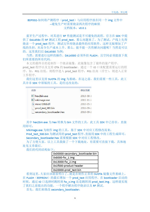
FLASH存储芯片作为软件升级使用。
(2)电源供电电路 电源电路使用220V供电,采用22OV转3. 3V电源模块,
并使用自恢复保险丝PTC,压敏电阻等保护器件,以确保 供电的稳定性和可靠性,电路图如下所示。
Fl PTC25O-O4O
图3电源供电电路
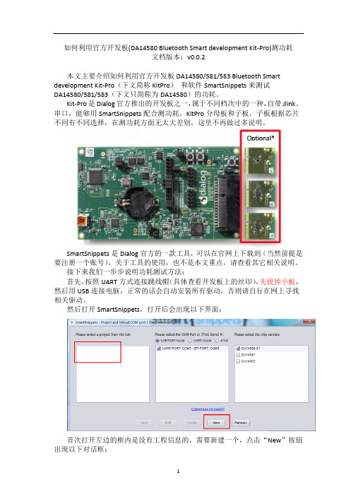
(3)白炽灯控制电路 采用可控硅⑷BTA08控制白炽灯的开与关,BTAO8是大功 率半导体器件,可满足一般灯具的功率要求。电路图如下所示。
表1车辆主要参数及设计目标
车辆主要参数
设计目标
整备质量(kg)
1150
最髙车速(km/h)
ห้องสมุดไป่ตู้
最大总质量(kg) 迎风面积(n?)
1550 2. 07
0〜50km/h加速时间(s) 50〜80km/h加速时间(s)
风阻系数
0. 33
最大爬坡度(%)
滚动阻力系数
0. 012
NEDC续驶里程(km)
滚动半径(m)
图1程序流程图面
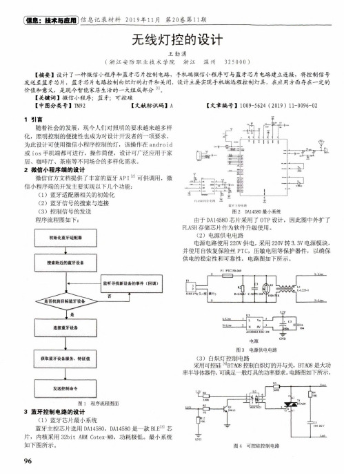
3蓝牙控制电路的设计 (1)蓝牙芯片最小系统
蓝牙主控芯片选用DA14580, DA14580是一款BLE[31芯 片,内核釆用32bit ARM Cotex-MO,功耗极低。最小系统 如下图所示。
96
图4可控硅控制电路
DA14580开发时如何将prod_test与应用程序放在同一个img文件中,以避免生产时需要烧录两次程序的麻烦
BDF002-如何将产测程序(prod_test)与应用程序放在同一个img文件中--避免生产时需要烧录两次程序的麻烦文档版本:v0.0.1蓝牙生产过程中,对其进行RF性能测试是不可避免的流程,官方在SDK中提供了DA1458x的RF测试工程prod_test,那么问题来了,为了测试,产线上先得烧录一个prod_test程序,测试完毕再烧录最终的应用软件,这样无疑增加了产线的负担,从而令生产成本上升。
那么,能不能一次性解决问题呢?当然是可以的。
这里我们以DA14580为例:当然,需要进行这样的操作,DA14580必须外挂FLASH,且空间必须能放下我们所需要的所有代码。
本文的最终目的是制作一个烧录镜像,此镜像包含了最终的量产程序、prod_test程序以及支持OTA的bootloader,通过一个IO口来配置需要运行的程序,如:P01拉低,则程序进入prod_test程序;P01拉高(浮空),则进入正常工作程序。
我们这里以支持SUOTA的img为基础,在这之前,我们需要一些工具,此工具并非SDK中原版的工具,是经过改良的:其中hex2bin.exe为hex转换为bin文件的工具,此工具SDK中已存在,直接用即可;Mkimage.exe为制作img的工具,基于SDK中对应工程修改而来;Prod_test_580.bin为测试用的prod_test程序,直接用SDK中的工程生成即可;Secondary_bootloader.hex需要根据SDK中对应工程修改。
为了方便大家,以上工具我做了一个下载地址,有需要可直接下载,具体地址见文章最后。
看到这里,镜像文件基础上,在FLASH(EEPROM)的最后增加一个prod_test应用程序,在bootloader启动的时候,通过IO口选择时跳转到fw_x.img还是跳转到prod_text.img。
这样就实现了我们之前提出的功能,一个程序解决程序烧录以及RF测试。
如何利用官方开发板(DA14580 Bluetooth Smart development Kit-Pro)测功耗
如何利用官方开发板(DA14580 B luetooth S mart d evelopment K it-‐Pro)测功耗文档版本:v0.0.2本文主要介绍如何利用官方开发板DA14580/581/583 B luetooth S mart development K it-‐Pro(下文简称KitPro) 和软件SmartSnippets来测试DA14580/581/583(下文只简称为DA14580)的功耗。
Kit-‐Pro是Dialog官方推出的开发板之一,属于不同档次中的一种,自带Jlink、串口,能够用SmartSnippets配合测功耗。
KitPro分母板和子板,子板根据芯片不同有不同选择,在测功耗方面无太大差别,这里不再做过多说明。
SmartSnippets是Dialog官方的一款工具,可以在官网上下载到(当然前提是要注册一个账号),关于工具的使用,也不是本文重点,请查看其它相关说明。
接下来我们一步步说明功耗测试方法:首先,按照UART方式连接跳线帽(具体查看开发板上的丝印),先拔掉小板,然后用USB连接电脑,正常的话会自动安装所有驱动,否则请自行在网上寻找相关驱动。
然后打开SmartSnippets,打开后会出现以下界面:首次打开左边的框内是没有工程信息的,需要新建一个,点击“New”按钮出现以下对话框:Project N ame随便输入一个,然后点“Save”。
选择刚刚创建的Project,并按照下图选择,最后“Open”。
打开后出现以下界面(可能会不同),选择左侧第一个图标,会打开“Board Setup”对话框,确保串口选择的是“P0_4,P0_5”.选择左边第三个按钮出现“Power P rofiler”对话框,点击下面的“Initialize”按钮。
然后点击“Start”:这时软件会运行,查看右上角“Avg C urret”下的数值并记下:点击“Stop”,然后点击“Config”:在新出来的对话框中,“Calibration O ffset”中填入刚刚记录的数值的负数,前面测出来的值是板子的电流(不包含DA14580小板,前面已经拔掉啦,如果没拔掉,那拔掉重测),因为我们要测的是小板的电流,所以这个主板电流需要减去。
亿佰特(Ebyte)-基于Dialog公司的DA14580的E104-BT02模块使用说明书

产品概述E104-BT02是一款超高性价比的1mW(0dBm)串口转BLE模块,使用PCB天线。
工作在2.4GHz频段。
模块可使用串口收发蓝牙数据,降低了蓝牙应用的门槛。
E104-BT02模块是基于Dialog公司的DA14580芯片研发,模块集成了透传功能、主从一体,即拿即用。
支持串口指令配置模块参数和功能,广泛应用于穿戴设备、家庭自动化、家庭安防、个人保健、智能家电、配饰与遥控器、汽车、照明、工业互联网等领域,模块具有稳定性高和超低的睡眠功耗,从机模式最低工作电流2uA以下(开启广播功能),可实现纽扣单电池供电。
数据传输稳定高效,从机模式下,支持波特率最大19200bps的数据连传功能,是一款名副其实的数据透传模块。
E104-BT02模块支持BluetoothV4.2标准,简单配置后可与符合蓝牙4.2协议的主机建立蓝牙连接,实现串口数据透传。
模块支持主从角色配置,支持主从模块点对点连接实现数据快速透传功能。
最大限度减少开发者的工作和项目开发时间。
目录产品概述 (3)1.产品特点62.典型应用: (6)3.技术参数74.机械特性85.功能简述95.1.封装95.2.推荐连线图95.3.工作模式95.4.数据有效指示 (10)5.5.角色切换105.6.MAC地址绑定 (10)5.7.串口连传105.8.蓝牙包长配置 (10)5.9.UUID配置115.10.蓝牙嗅探115.11.B EACON数据可切换 (11)5.12.空中配置126.操作指令126.1.模块复位指令 (13)6.2.恢复出厂模式 (13)6.3.串口波特率配置指令 (13)6.4.读串口波特率指令 (13)6.5.串口停止位配置指令 (14)6.6.读串口停止位指令 (14)6.7.串口校验位配置指令 (14)6.8.读串口校验类型 (14)6.9.开启广播指令 (14)6.10.停止广播指令 (14)6.11.查询广播状态 (14)6.12.设置普通广播数据 (15)6.13.设置IB EACON广播数据 (15)6.14.设置固定广播数据 (15)6.15.设备名设置156.16.读设备名156.17.设置厂商名156.18.读厂商名156.19.设置软件版本号 (16)6.20.读软件版本号 (16)6.21.设置硬件版本号 (16)6.22.读硬件版本号 (16)6.23.设置模块SN号 (16)6.24.读模块SN号 (16)6.25.设置S YSTEM ID (16)6.26.查询S YSTEM ID (17)6.27.设置模块编号 (17)6.28.查询模块编号 (17)6.29.设置广播间隙 (17)6.30.读广播间隙176.31.设置最大连接间隙 (17)6.32.读最大连接间隙 (17)6.33.设置最小连接间隙 (18)6.34.读最小连接间隙 (18)6.35.设置连接超时 (18)6.36.读连接超时186.37.断开当前连接 (18)6.38.查询蓝牙连接状态 (18)6.39.查询本地MAC地址 (18)6.40.查询已连接设备MAC地址 (19)6.41.设置绑定连接的MAC地址 (19)6.42.读设定的绑定MAC地址 (19)6.43.关闭MAC地址过滤 (19)6.44.开启模式反馈 (19)6.45.关闭模式反馈 (19)6.46.启动扫描196.47.停止扫描206.48.读扫描状态206.49.设置扫描间隙 (20)6.50.查询扫描间隙 (20)6.51.设置扫描窗口时间 (20)6.52.查询扫描窗口时间 (20)6.53.开启嗅探功能 (20)6.54.关闭嗅探功能 (21)6.55.读取当前RSSI值 (21)6.56.打开128BIT UUID显示 (21)6.57.关闭128BIT UUID显示 (21)6.58.设置服务名UUID (21)6.59.设置RXUUID (21)6.60.设置TXUUID216.61.设置MTU长度 (22)6.62.查询MTU长度 (22)6.63.查询设备角色 (22)6.64.串口唤醒开226.65.串口唤醒关226.66.开启数据输出指示 (22)6.67.关闭数据输出指示 (22)6.68.进入休眠后关闭蓝牙连接 (23)6.69.进入休眠后保持蓝牙连接 (23)6.70.空中配置密码认证 (23)6.71.空中配置密码更新 (23)7.UUID说明 (23)8.快速使用239.生产指导2710.常见问题2811.重要声明2812.关于我们错误!未定义书签。
(软件著作权申报材料模板)软件设计说明书
目录1、引言 (1)1.1、编写目的 (1)1.2、定义 (1)1.3、参考资料 (1)2、设计概述 (1)2.1、设计任务 (1)2.2、设计约束和限制 (2)3、总体设计 (2)4、模块描述 (3)4.1、陀螺仪模块 (3)4.1.1、电源管理 (3)4.1.2、数据采样 (4)4.2、降噪模块 (7)4.3、电量检测模块 (7)4.4、指示灯模块 (8)4.4.1、红色指示灯 (8)4.4.2、绿色指示灯 (8)4.5、微信服务模块 (9)4.5.1、模块概述 (9)4.5.2、软件流程 (12)1、引言1.1、编写目的本设计说明书针对XXXX智能耳机(以下简称智能耳机)的底层驱动软件而编写。
目的介绍系统的各个模块,为进行后面的实现作准备。
1.2、定义MCU:MicroController UnitBLE:Bluetooth Low EnergySDK:Software Development Kit1.3、参考资料设备接入接口协议V2.3微信蓝牙外设协议1.0.4微信硬件平台技术方案微信硬件平台介绍微信硬件平台框架说明及接入流程微信硬件平台蓝牙demo需求XXXX智能耳机MCU软件需求说明书UM-B-003_DA14580_Software_development_guideUM-B-014_DA14580_Development_KitUM-B-015_DA14580_Software_architecture2、设计概述2.1、设计任务智能耳机首先是一款耳机,然后才是通过蓝牙与微信客户端连接实现更多的扩展功能。
所以MCU软件需要实现两方面的功能,向下驱动底层硬件并实现逻辑控制,向上通过蓝牙跟微信客户端通信并实现扩展功能,如图2-1。
图2-1 设计任务2.2、设计约束和限制MCU:dialog DA14580蓝牙:4.0 BLE编程语言:C语言3、总体设计为了节省开发时间,使用dialog官方SDK(以下简称“SDK”)开发。
DA14580术语和定义
BLE Bluetooth low energy 蓝牙低功耗GAP Generic Access Profile 通用接入规范GATT Generic Attribute Profile 通用属性配置文件GTL Generic Transport Layer 通用传输层HCI Host Controller Interface 主机控制接口RSSI Received Signal Strength Indicator 接受信号强度指示器SDK Software Development Kit 软件开发包URX UART Receive port UART接收端口UTX UART Transmit port UART发送接口(S)RAM (Static) Random Access Memory (静态)随机存取存储器UUID Universal Unique ID 通用唯一IDISR Interrupt Service Routine 中断服务器例程GAPM Generic Access Profile Manager 通用访问配置文件管理器DK Development Kit 开发工具AON Always ON 一直打开API Application Programming Interface 应用程序接口ISR Interrupt Service Routine 中断服务器例程OS Operating System 操作系统RAM Random Access Memory 随机存储器RC16M 16MHz clock generated by internal oscillator 内部振荡器产生16MHZ时钟ROM Read Only Memory 只读存储器WFI Wait For Interrupt instruction 等待中断指令XTAL16M 16MHz crystal 16MHZ晶振DTM Direct Test Mode for Bluetooth Devices 蓝牙设备直接测试模式EUT Equipment Under Test 被测试设备SPOTAR SPotA ReceiverSPOTAI SPotA InitiatorRETRAM Retention RAM 保留内存BLE SIG Bluetooth Low Energy Special Interest GroupMSB Most Significant Byte 最高有效字节LSB List Significant Byte 列出有限字节CLI Command Line Interface 命令行接口GUI Graphical User Interface 图形用户界面HCI Host Controller Interface 主机控制接口XTAL16M 16 MHz Crystal 16 MHz晶振XTAL32K 32 KHz Crystal 32 KHz晶振RC16M 16 MHz RC Oscillator 16MHZ RC振荡器RC32K 32 KHz RC Oscillator 32KHZ RC振荡器Retention RAM Memory that is powered when DA14580 is in Deep sleepRO section Memory section where code (RO) is placedRW section Memory section where global initialized variables are placedScatter file Text file used to specify the memory map of an image to the linkerZI section Memory section where zero initialized variables are placedDMA Direct Memory Access 直接存储器(内存)访问FSM Finite State Machine 有限状态机LDO Low Drop-Out (regulator) 低漏失(校准器) SUOTA Software Update Over The AirDREADY Data ReadyFTDI Quad-Flat No-leadsQFN Quad-Flat No-leadsSRAM Static Random Access MemoryUTX Quad-Flat No-leadsURX Quad-Flat No-leadsURTS Quad-Flat No-leadsUCTS Quad-Flat No-leadsUCTS Quad-Flat No-leadsWLCSP Wafer Level Chip Scale PackagingGAP Generic Access ProfileGTL Generic Transport LayerHCI Host Controller InterfaceNVDS Non-V olatile Data StorageSoC System-on-ChipSPotA Software Patching over the AirCTS Clear To SendRTS Request To SendCLI Command Line InterfaceDUT Device Under TestRF Radio FrequencyIR Infra RedUV Ultra VioletDTM Bluetooth Direct Test ModeWLCSP Wafer Level Chip Scale PackageIRK Identity Resolving KeyLTK Long Term KeyMSB Most Significant BitsMITM Man In The MiddleFOSS Free and Open-Source SoftwareGDB GNU DebuggerIDE Integrated Development EnvironmentKiB Kbyte (1024 bytes)LTO Link-Time OptimisationBTLE Bluetooth Low EnergyPWM Pulse Width ModulationRAM Random Access MemoryROM Read Only MemoryNVIC Nested Vector Interrupt ControllerSysRAM System RAMRetRAM Retention RAMCTS Clear To SendGTL Generic Transport LayerRTS Request To SendIFA Inverted-F AntennaPIFA Planar Inverted-F AntennaRC Remote ControlGTL Generic Transport LayerDISS Device Information Service Server 设备信息服务服务器HAL Hardware Adaptation Layer 硬件适用层。
(DA14580_bootloader)官方手册
Company confidentialUser manualDA14580 Creation of a secondaryboot loaderUM-B-012AbstractThis document provides an overview of the booting sequence of the DA14580 and it describes the implementation steps for the development of a secondary boot loader application An extension of the secondary boot loader to support a dual boot images scheme is also presented.ContentsContents (2)Figures (2)Tables (2)1 Terms and definitions (3)2 References (3)3 Introduction (4)4 How DA14580 Boots (4)5 Secondary Boot loader application (4)5.1Booting from SPI master (4)5.2Booting from UART (4)5.3Booting from SPI (5)5.4Booting from an I2C/EEPROM (6)6 Dual Image Bootloader (6)6.1Non-volatile memory map (6)6.2Booting Sequence (8)6.3How to prepare the non-volatile memory (8)7 Application Description (9)7.1System Initialization (9)8 Getting Started (12)8.1Writing application HEX file to SPI Flash (12)Writing boot loader HEX file to OTP memory (13)8.28.3Measuring the booting time (13)9 Revision history (15)FiguresFigure 1: Non-volatile memory map (7)Figure 2: File Structure (10)Figure 3: SPI Flash Programmer (12)Figure 4: OPT Prograrmmer (13)Figure 5: Booting sequence using the secondary loader (14)Figure 6: Normal booting sequence (14)TablesTable 1: Transmission sequence (5)Table 2: SPI Header (5)Table 3: EEPROM Header (6)Table 4: Product header format (7)Table 5: Image header format (8)1 Terms and definitionsEEPROM Electrically Erasable Programmable MemoryGPIO General Purpose Input OutputOTP One Time Programmable (memory)SDK Software Development KitSPI Serial Peripheral InterfaceSUOTA Software Update Over The AirUART Universal Asynchronous Receiver/TransmitterURX UART Receive portUTX UART Transmit port2 References1. DA14580 Datasheet, Dialog Semiconductor.2. AN-B-001, Booting from Serial Interfaces, Dialog Semiconductor3. UM-B-014, DA14580 Development Kit, Dialog Semiconductor.4. UM-B-003, DA14580 Peripherals Drivers, Dialog Semiconductor.5. UM-B-009, DA14580 Proximity Application, Dialog Semiconductor.6. AN-B-023, DA14580 interfacing with external memory, Dialog Semiconductor3 IntroductionThis document provides an overview of the booting sequence of DA14580 and describes the steps for creating a secondary bootloader application. The application structure, the steps for testing it and a methodology for measuring the booting time are presented.The secondary boot loader allows DA14580 to boot from a SPI or EEPROM flash memory or UART interface. It can be used to replace the ROM boot loader in case a faster booting sequence is needed.An extension of the secondary bootloader based on dual images is also represented in this document. The dual image bootloader can be used together with the Software Upgrade Over The Air (SUOTA) application for the product firmware upgrade.4 How DA14580 BootsDA14580 operates in two modes [1, 2], namely the “Normal Mode” and the “Development/Calibration Mode” hereafter address as “DevMode”.At power up or reset of the DA14580, the primary boot code (ROM code) will check if the OTP memory is programmed. When this is the case the DA14580 enters “Normal Mode”. It proceeds with mirroring the OTP contents to System RAM and it will program execution.Otherwise, it enters “DevMode”. It scans a predefined number of pins to communicate with external devices, using the three interfaces available on chip:∙UART,∙SPI,∙I2C.Due to the time it requires to scan the interfaces (SPI as slave, UART, SPI as master and I2C) in DevMode the start-up time is longer than in Normal Mode. The difference in start-up time is around a few milliseconds in Normal Mode to several decades of milliseconds in DevMode [2].For applications requiring to run from an empty OTP and at the same time have a short boot time a dedicated secondary loader can be developed, that will skip the long sequence of scanning interfaces. Such a dedicated secondary loader will start communicating directly on a selected interface to download instead of DevMode.The flow chart of the booting is shown in Error! Reference source not found.5 Secondary Boot loader applicationIn this section three use cases of the secondary bootloader are described: booting form UART interface, booting from EEPROM and booting from SPI flash.5.1Booting from SPI masterIt is possible for a host controller to act as a SPI master. In this case the DA14580 is the SPI slave. Via the host controller the booting can take place.No further details are mentioned now, about this way of booting.5.2Booting from UARTThe secondary loader application reads the UART RX Pin status with GPIO_GetPinStatus() command and if it is high (1), it starts the booting procedure from the UART interface.The protocol for booting from UART is the same [2], as that of ROM boot code and it is implemented in function FwDownload() (uart_booter.c).It starts with the DA14580 UART TX pin transmitting 0x02 (Start TX, STX). The external device is expected to answer a 0x01 (Start of Header, SOH) byte followed by 2 more bytes (LEN_LSB,LEN_MSB) which defines the length of the code to be downloaded (first byte is the least significant, second byte is the most significant). The DA14580 answers with 0x06 (ACK) if 3 bytes have been received and SOH identified or with 0x15 (NACK) if anything went wrong or the size if greater that the expected one.Table 1: Transmission sequenceAt this point connection has been successfully established and the SW code will start being downloaded. The next N bytes are received and placed into the System RAM.Following the completion of the required code bytes, the boot code will calculate the CRC and send it over the UART. The booting sequence ends with by reading the value 0x06 (ACK) at the URX line. CRC is calculated by XORing every successive byte with the previous value. Initial CRC value is0x00.During the final step of the boot code, the UART GPIO pins are initialized to the default state.SYS_CTRL_REG is programmed to Remap to System RAM and apply a SW reset or perform a branch to System RAM. It is depended of the base address of the application code, so the system starts executing the code.Booting from UART method can be used by the user to download the flash programmer application in order to upgrade the application firmware stored in SPI flash. This option is provided by the SPI programmer tool of Smart Snippets.5.3Booting from SPIThe secondary boot loader application initializes the SPI interface and the SPI flash memory if no UART is detected the options SPI_FLASH_SUPPORTED and SUPPORT_AN_B_001 are defined in the file bootloader.h. Then, it checks if the header described in AN-B-001 [2] (Table 2) is present by checking the first two bytes of the header for the signature (0x70, 0x50) and if a valid header is detected it copies a number of bytes equal to Code Size to System Ram and starts the user application.Table 2: SPI Header5.4Booting from an I2C/EEPROMThe secondary boot loader application initials the I2C/EEPROM flash memory if no UART is detected and the option EEPROM_FLASH_SUPPORTED and SUPPORT_AN_B_001 are defined in the file bootloader.h. Then, it checks if the header described in AN-B-001 (Table 2) is present by checking the first two bytes of the header for the signature (0x70, 0x50) and if a valid header is detected it copies a number of bytes equal to Code Size to System Ram. Finally, it verifies the checksum of the code data and if it matches the CRC field of the header and starts the user application.Table 3: EEPROM Header6 Dual Image BootloaderThis section describes an extension of the secondary boot loader to support a dual image bootloader scheme which is used in SUOTA application for the product firmware upgrade in the field.6.1Non-volatile memory mapThe non-volatile memory map to meet the needs of the dual image bootloader scheme is represented in Figure 1.The first part is the boot loader , in case it’s stored in the nonThe images with the corresponding headers are stored at offset #1 and offset #2 which are defined in the product header. The product header is suggested to be programmed at the last sector of the non-volatile memory.Figure 1: Non-volatile memory mapNote 1 The bootloader is stored either in the first sector of the non-volatile memory according to AN-B-001 or in OTP flash memory.The product header (Table 3) defines the addresses of the two firmware images stored in the non-volatile memory. It is programmed in the production line and the corresponding flash sector may be protected if it’s supported by the flash characteristics.■signature (0x70, 0x52): It is a magic number identifying the product header .■version:Two bytes reserved for the versioning of the product header■offset #1: It defines the address of the first image stored in non-volatile memory. Four bytes in Little Endian format.■offset #2: It defines the address of the second image stored in non-volatile memory. Four bytes in Little Endian format.Note 2 The product header may contain more information or configuartion settings i.e. NVDS data , DB address, XTAL16 trim settings. The use of these parameter is explained in the [6].Table 4: Product header formatThe image header includes the following fields as shown in Figure XX:■signature (0x70, 0x51): It is a magic number identifying the image header■validflag: The validation field. It identify if the image has been downloaded correctly and the checksum has been verified. The value 0xFF defines a new image, the 0xAA defines a valid image and any other value defines an invalid image.■imageid: An increment counter which defines the active image.■code_size: It defines the size of the firmware image.■CRC: It defines the checksum calculated over the image data.■version: A 16 bytes string is used for the image version.■timestamp: It defines the image creation time based on seconds since standard epoch of 1/1/1970.Table 5: Image header format6.2Booting SequenceDuring the booting phase, the bootloader checks the product header and reads the addresses of the two images stored in the non-volatile memory and reads the contents of the two image header to find out the valid image with the greater imageid and load it to system ram if the checksum of the code data matches the value of the CRC header field.6.3How to prepare the non-volatile memorySmart Snippets tool can be used for burning the bootloader in non-volatile memory or OTP and the product header and the dual images in the non-volatile memory.For example, the SPI memory preparation is done in 3 steps. The steps are described below:1. Program the product header (0x1F000):Create a text file to describe the product header as shown below , load it using the Memory header option of the SmartSnippets toolkit, enter the following values in the product header fields Signature: 0x70, 0x52Version: 1234Offset1: 00800000 (it corresponds to offset 0x8000)Offset2: 00300100 (it corresponds to offset 0x13000)and burn it to SPI flash at address 0x1F000. For more information how to create the product header refer to HELP menu of the SmartSnippets toolkit.2 Signature MagicNumber2 Version VersionNumber4 Offset1 Offset_image_14 Offset2 Offset_image_22. Program the image binaries:Build the integrated processor proximity reporter application and convert the HEX to BIN file. Use the mkimage tool (located in tools\mkimage of the SDK distribution) to convert the BIN to IMG file. For more information how to use this tool, run mkimage without arguments.Load the image.img file using the SPI Flash Programmer option of the SmartSnippets toolkit and burn it to SPI flash at address 0x8000 (image #1) and 0x13000 ((image #2).3. Program the bootloader:Build the secondary_bootloader as described below and burn the HEX file at address 0x0 using the SPI Flash Programmer option of the SmartSnippets toolkit. (Select ‘Yes’, in the question to make the SPI memory bootable.)7 Application Description7.1System InitializationThe secondary loader application executes in the retention memory in order the System Ram memory to be available for storing the application data when the system boots either form UART or SPI interface. It sets the system clock and memory configuration as below:SetWord16(CLK_AMBA_REG, 0x00); //fastestSetBits32(GP_CONTROL_REG, EM_MAP, 7);SetBits16(PMU_CTRL_REG, RETENTION_MODE, 0xF);In the main function, secondary loader disables the Watch dog timer, sets all the peripherals in active mode and waits until the system is ready:SetWord16(SET_FREEZE_REG,FRZ_WDOG); // disable Watch DogSetBits16(PMU_CTRL_REG, PERIPH_SLEEP,0); // exit peripheral power downwhile (!(GetWord16(SYS_STAT_REG) & PER_IS_UP)); // Power up peripherals' power domain For special designs when the system must work at 1.8Voltage, the following command must be enabled.#ifdef SUPPORT_1_8_VSetBits16(DCDC_CTRL2_REG, DCDC_VBAT3V_LEV, 0x0); ///--Support 1.8V boot#endifNext, the application detects the UART RX pin level and decides whether the UART or SPI booting function will be performed.The file structure of the secondary_bootloader project is shown in Figure 2.System initialization files: startup_CMSDK_CM0.s, system_CMSDK.c, bootloader.sct and sysram.ini are included in folder secondary_bootloader/boot.Figure 2: File Structure∙startup_CMSDK_CM0.s: The startup file for ARM Cortex-M0. It contains stack and heap configuration and the vector table.∙system_CMSDK.c : It contains the functions which initializes the system and update the SystemFrequency variable.∙bootloader.sct : It is the scatter-Loading description file∙sysram.ini: Keil debugger init script.∙Source files (.c): main.c,bootloader.c, uart_booter.c, timer.c and uart.c spi_commands.c crc32.c are included in the folder secondary_bootloader/src. Drivers files spi.c, spi_flash.c and gpio.c are located in folder dk_apps\src\plf\refip\src\driver\∙main.c: It contains the main function, system initialization function and the main loop of the application.∙bootloader.c: It contains the functions for booting from SPI and EEPROM and the implementation of the dual image bootloader.∙Uart_booter.c: It contains the functions for booting from UART.∙timer.c. In this file the timer functions are implemented. A software timer is used for the timeouts required by the UART boot protocol.∙spi_commands.c; It contains the additional commands for accessing the SPI flash.∙spi.c, spi_flash.c, gpio.c: Peripherals Drivers for SPI , SPI flash and GPIO interfaces.Detailed information for the drivers can be found in [3].∙Include files (.h): periph_setup.h, timer.h and uart.h are included in the folder secondary_bootloader/includes.∙periph_setup.h: This file contains the configuration settings for the peripherals (UART, SPI, SPI flash) used by the secondary boot loader application.The main configuration settings are listed below:// Select EEPROM characteristics#define I2C_EEPROM_SIZE 0x20000 // EEPROM size in bytes#define I2C_EEPROM_PAGE 256 // EEPROM's page size in bytes#define I2C_SLAVE_ADDRESS 0x50 // Set slave device address#define I2C_SPEED_MODE I2C_FAST // 1: standard mode (100 kbits/s), 2: fast mode (400 kbits/s)#define I2C_ADDRESS_MODE I2C_7BIT_ADDR // 0: 7-bit addressing, 1: 10-bit addressing #define I2C_ADDRESS_SIZE I2C_2BYTES_ADDR // 0: 8-bit memory address, 1: 16-bit memory address, 3: 24-bit memory address// SPI Flash settings// SPI Flash Manufacturer and ID#define W25X10CL_MANF_DEV_ID (0xEF10) // W25X10CL Manufacturer and ID#define W25X20CL_MANF_DEV_ID (0xEF11) // W25X10CL Manufacturer and ID// SPI Flash options#define W25X10CL_SIZE 131072 // SPI Flash memory size in bytes#define W25X20CL_SIZE 262144 // SPI Flash memory size in bytes#define W25X10CL_PAGE 256 // SPI Flash memory page size in bytes#define W25X20CL_PAGE 256 // SPI Flash memory page size in bytes#define SPI_FLASH_DEFAULT_SIZE 131072 // SPI Flash memory size in bytes#define SPI_FLASH_DEFAULT_PAGE 256 // SPI Flash memory page size in bytes//SPI initialization parameters#define SPI_WORD_MODE SPI_8BIT_MODE#define SPI_SMN_MODE SPI_MASTER_MODE#define SPI_POL_MODE SPI_CLK_INIT_HIGH#define SPI_PHA_MODE SPI_PHASE_1#define SPI_MINT_EN SPI_NO_MINT#define SPI_CLK_DIV SPI_XTAL_DIV_2// UART GPIOs assignment#define UART_GPIO_PORT GPIO_PORT_0#define UART_TX_PIN GPIO_PIN_4#define UART_RX_PIN GPIO_PIN_5#define UART_BAUDRATE baudrate_57K6// SPI GPIO assignment#define SPI_GPIO_PORT GPIO_PORT_0#define SPI_CS_PIN GPIO_PIN_3#define SPI_CLK_PIN GPIO_PIN_0#define SPI_DO_PIN GPIO_PIN_6#define SPI_DI_PIN GPIO_PIN_5// EEPROM GPIO assignment#define I2C_GPIO_PORT GPIO_PORT_0#define I2C_SCL_PIN GPIO_PIN_2#define I2C_SDA_PIN GPIO_PIN_3W25X10CL SPI flash is supported. The W25X10CL arrays are organized into 512 programmable pages of 256-bytes each. Up to 256 bytes can be programmed at a time. The W25X10CLhave 32 erasable sectors, 4 erasable 32KB blocks and 2 erasable 64KB blocks respectively. The W25X20CL SPI flash is also supported.Other SPI Flash types can be supported by changing above configuration settings (i.e.SPI_FLASH_SIZE, SPI_FLASH_PAGE etc.)GPIO Port 0 is used by default as it’s supported by all DA14580 types (WLCSP, QFN40 andQFN48).GPIO Pin 4 and 5 are assigned to UART TX and RX respectively.GPIO Pin 0, 3, 5 and 6 are assigned to SPI CS, CLK, DI and DO respectively.The conflict in GPIO Pin 5 is solved by sequential access to it from UART and SPI interface.8 Getting StartedThis section describes how to program the secondary bootloader and an application (i.e. integrated proximity reporter) in the SPI flash or the OTP memory and measure the system booting time. A comparison with normal booter (ROMbooter) is also provided.Smart Snippets toolkit supports tools for SPI Flash and OTP memory programming. The SPI Flash must be programmed with proximity application and the OTP memory with boot loader application.8.1Writing application HEX file to SPI FlashSmart Snippets SPI Flash Programmer is used for downloading an image file to the DA14580 SPI Flash Memory. Figure 2 shows the main screen of the SPI Flash programmer tool.The following three steps are required for preparing the Proximity Reporter application:Open Proximity Reporter project, dk_apps\keil_projects\proximity\reporter_fh.Figure 3: SPI Flash ProgrammerCompile Proximity Reporter Application to generate the executable file full_emb_sysram.hex.Open Smart Snippets and burn full_emb_sysram.hex to SPI Flash memory at offset 0x20. Header is automatically added by the Flash programmer firmware. SPI flash bootable for optimizing the boot time as the boot loader will copy only the actual application data written in SPI header. Make SPI flash non bootable to measure the max booting time as boot loader will copy 32KB from SPI flash.8.2Writing boot loader HEX file to OTP memoryOTP programmer tool enables downloading the default firmware into the System RAM and burning the OTP memory with a user-defined HEX and BIN file. Figure 3 shows the main screen of the OPT programmer.Figure 4: OPT PrograrmmerCompile the project to generate the executable file secondary_bootloader.hexThe following steps are required for programming the executable secondary_bootloader.hex in OTP memory:Open Smart Snippets applicationburn secondary bootloader.hex in OTP imageEnable Application Flag 1 and Application Flag 2, set DMA Length and burn OTP headerNote 3 J12 and J25 must be connected for OTP burning and UART interface, respectively. Make sure 6.8V is connected to the VPP pin. When doing this on the Dialog hardware development kit [3].8.3Measuring the booting timeThis section describes the procedure for measuring the booting time of an application stored in SPI flash with the secondary boot loader described in this document and it’s compared with the time required with the normal loader stored n ROM.The Power Profiler tool of the Smart Snippets toolset is used to measure the time takes between power up and first advertising point.In Figure 4, the booting time of the Proximity application with the secondary loader is shown. The point A corresponds to DA14580 power up time, point B corresponds to the first advertising point, points C and D illustrate the start and end point of the application data transfer from SPI to the system RAM and point C corresponds to the first application entry point (main()). The time required until the first advertisement is 158.8msec. The data transfer from the SPI flash takes 36msec (Note 2) and the time required until the first application entry point is 145msec.Note 4 32KB data transferred instead of the actual application data size.In Figure 5, the booting time of the Proximity application with the normal booting sequence is shown. The point A corresponds to DA14580 power up time, point B corresponds to the first advertising point, points C and D illustrate the start and end point of the application data transfer from SPI to the system RAM and point C corresponds to the first application entry point (main()). The time required until the first advertisement is 309.47msec. The data transfer from the SPI flash takes 100msec and the time required until the first application entry point is 295msec.The secondary loader achieves faster boot time as it skips the scanning sequence of the normal mode while the SPI operation is optimized for the specific used SPI flash.Figure 5: Booting sequence using the secondary loaderFigure 6: Normal booting sequence9 Revision historyStatus definitionsDisclaimerInformation in this document is believed to be accurate and reliable. However, Dialog Semiconductor does not give any representations or warranties, expressed or implied, as to the accuracy or completeness of such information. Dialog Semiconductor furthermore takes no responsibility whatsoever for the content in this document if provided by any information source outside of Dialog Semiconductor.Dialog Semiconductor reserves the right to change without notice the information published in this document, including without limitation the specification and the design of the related semiconductor products, software and applications.Applications, software, and semiconductor products described in this document are for illustrative purposes only. Dialog Semiconductor makes no representation or warranty that such applications, software and semiconductor products will be suitable for the specified use without further testing or modification. Unless otherwise agreed in writing, such testing or modification is the sole responsibility of the customer and Dialog Semiconductor excludes all liability in this respect. Customer notes that nothing in this document may be construed as a license for customer to use the Dialog Semiconductor products, software and applications referred to in this document. Such license must be separately sought by customer with Dialog Semiconductor.All use of Dialog Semiconductor products, software and applications referred to in this document are subject to Dialog Semiconductor’s Standard Terms and Conditions of Sale, unless otherwise stated.© Dialog Semiconductor GmbH. All rights reserved.RoHS ComplianceDialog Semiconductor complies to European Directive 2001/95/EC and from 2 January 2013 onwards to European Directive 2011/65/EU concerning Restriction of Hazardous Substances (RoHS/RoHS2).Dialog Semiconductor’s statement on RoHS can be found on the customer portal https:///. RoHS certificates from our suppliers are available on request.Contacting Dialog SemiconductorGermany Headquarters Dialog Semiconductor GmbH Phone: +49 7021 805-0United KingdomDialog Semiconductor (UK) Ltd Phone: +44 1793 757700The NetherlandsDialog Semiconductor B.V. Phone: +31 73 640 8822 North AmericaDialog Semiconductor Inc.Phone: +1 408 845 8500JapanDialog Semiconductor K. K.Phone: +81 3 5425 4567TaiwanDialog Semiconductor TaiwanPhone: +886 281 786 222SingaporeDialog Semiconductor SingaporePhone: +65 64 849929ChinaDialog Semiconductor ChinaPhone: +86 21 5178 2561KoreaDialog Semiconductor KoreaPhone: +82 2 3469 8291Email: Web site:。
DA14580 蓝牙模块
蓝牙4.1 低功耗BLE 模块YH-001_V1.01(主芯片Dialog_ DA14580)模块概述YH-001_V1.01 是一个蓝牙4.1 单模低功耗(BLE)数传模块,高度集成了蓝牙低功耗射频、协议栈、profile 以及应用程序于系统级芯片DA14580 (内置蓝牙+ARMcortex-M0),它不仅无需外接MCU,而且提供足够的I/O 用于硬件设计和程序开发,非常适合应用于需要超低功耗的系统上。
主要特性1.蓝牙4.1 单模低功耗模块2.完美支持主从模式(Master/Slave)3.集成蓝牙低功耗BLE 协议栈16MHz/32bit ARM Cortex M0,无需要外接MCU4.内置AES-128bit 加密程序5.内置专用链路层处理器6.射频特性TX 功率:-20dBm 至0dBm RX 灵敏度:-93dBm7.通信传输有效距离:30M(无外置功放)8.处理器16MHz 32 位ARM Cortex M0,带有SWD 接口9.内存32kB 的一次性可编程(OTP)闪存42K SRAM 84kB ROM 8kB 保留SRAM10. 工作电压典型值3.0V 建议范围 2.5V-3.3V (支持普通7 号、5 号和纽扣电池供电)11. RF 收发器3V 供电,理想状态TX:3.4mA RX:3.7mA12. 接口4 通道10 位ADC 2 个UART 接口SPI 接口I2C 接口PWM 输出20 通用I/O 接口13. 封装尺寸23.2mm * 17mm * 1.8mm应用领域:1.医疗保健设备2.运动及健康设备3.家庭智能设备4.手机和PC 配件5.工业自动化设备6. 物联网节点设备及网关7. 智能遥控器(含语音识别)8. 手机APP 控制互动玩具9. 手机APP 控制四轴飞行器10.HID 外设,键盘、鼠标……YH-001_V1.01 方框图YH001-V1.01电气特性:绝对最大额定值建议工作条件NOTE1:基于蓝牙芯片RAM 工作特性,要求蓝牙设备冷启动时VDD ≧2.5 V,所以建议模块供电稳定VDD=3V外形尺寸:YH-001_V1.01 的总体尺寸,长23.2 毫米,宽17 毫米,厚1.8 毫米。