Supertex LED driver workshop
超特克HV9910BDB7高亮LED驱动示例板说明书

Supertex inc.HV9910BDB7HV9910B PFC 40W LED Driver DemoboardSpecificationsActual Size: 3.0” x 2.3” x 1.1”Top View Bottom ViewGeneral DescriptionThe Supertex HV9910BDB7 demonstrates the use of an HV9910B control IC in an off-line, High Brightness LED driver application. The board incorporates power factor correction (PFC) and satisfies the limits for harmonic currents according to the EN61000-3-2 Class C standard having total harmonic distortion (THD) less than 20%. The board features a low component count and long life operation due to the absence of electrolytic capacitors. The board is designed to supply a string of LEDs with a current of 350mA and a voltage in the 65 to 105V range from a 220/230VAC line.The conversion stage draws line current throughout the AC line cycle, partly using a charge pumping and partly using a boost conversion technique to charge the bulk energy storage capacitors. The LED current is provided with a continuous mode buck stage giving a DC current with about 30% peak-to-peak ripple. A patent for this conversion technique is pending. Please inquire with the Supertex applications department for design guidance, should change of input line voltage, output voltage, or output current be desired.An effort was made to satisfy the requirements of CISPR 15 (EN55015), limits and methods of measurement of radio disturbance characteristics of electrical lighting and similar equipment.The connection diagram details the hookup of the board to the AC line. Note that the load is NOT galvanically isolated, and that measurements to the board require measurement techniques in common use with non-isolated off-line power supplies (isolation transformers, differential probes, etc).Board LayoutSchematic DiagramConnection Diagram220VAC105VDC 350mADCConnectionsI nput Voltage - Connect the AC line input voltage to AC VIN as shown.LED String - Connect the LED strings between LED+ and LED- as shown (anode of the string to LED+ and cathode to LED-).Figure 3. Load regulation.Figure 4. AC line regulation.Figure 6. Power Factor vs. AC Line Voltage.Figure 5. Harmonic Distortion vs. AC Line Voltage.ILoad Regulation (V = 230V )0.3480.3520.3540.3560.3580.3620.3640.366V OI Line Regulation (V = 105V)0.3490.3500.3510.3520.3530.3540.3550.3560.3570.358V ACHarmonic Distortion (V = 105V, I = 350mA)10152025303540V ACPower Factor (V = 105V, I = 350mA)V ACTypical CharacteristicsEfficiency (V = 105V, I = 350mA) V ACEfficiency (V = 230V , I = 350mA)V OFigure 1. Efficiency at full load.Figure 2. Efficiency at nominal AC line voltage.Figure 7. EMI Characterization - Conducted Emissions vs CISPR 15 Limits. Figure 8. CT1 Construction Diagram.Supertex inc. does not recommend the use of its products in life support applications, and will not knowingly sell them for use in such applications unless it receives an adequate “product liability indemnification insurance agreement.” Supertex inc. does not assume responsibility for use of devices described, and limits its liability to the replacement of the devices determined defective due to workmanship. No responsibility is assumed for possible omissions and inaccuracies. Circuitry and specifications are subject to change without notice. For the latest product specifications refer to the Supertex inc. (website: http//)©2013 Supertex inc.All rights reserved. Unauthorized use or reproduction is prohibited.Supertex inc.。
HV9911 大电流LED驱动设计资料
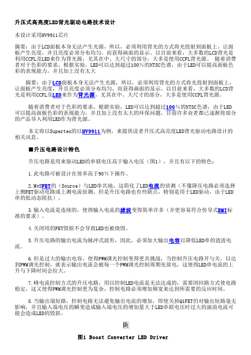
升压式高亮度LED背光驱动电路技术设计本设计采用HV9911芯片摘要:由于LCD面板本身无法产生光源,所以,必须利用背光的方式将光投射到面板上,让面板产生亮度,并且亮度必须分布均匀,而获得画面的显示。
以目前来看,大多数的LCD背光是利用CCFL及LED来作为背光源,尤其在中、大尺寸的部分,大多是使用CCFL背光源。
随着消费者对于色彩的要求,根据实验,LED可以达到超过100%的NTSC色谱,由于LED可以提高面板色彩的表现能力,并且加上没有太大 摘要:由于LCD面板本身无法产生光源,所以,必须利用背光的方式将光投射到面板上,让面板产生亮度,并且亮度必须分布均匀,而获得画面的显示。
以目前来看,大多数的LCD背光是利用CCFL及LED来作为背光源,尤其在中、大尺寸的部分,大多是使用CCFL背光源。
随着消费者对于色彩的要求,根据实验,LED可以达到超过100%的NTSC色谱,由于LED 可以提高面板色彩的表现能力,并且加上没有太大的环保问题。
目前许多业者都已逐渐将部分的产品导入利用LED作为背光源。
本文将以Supertex的以HV9911为例,来提供读者升压式高亮度LED背光驱动电路设计的相关讯息。
■升压电路设计特色 升压电路是用来驱动LED的串联电压高于输入电压(图1),并且有以下的特色: 1.此电路可被设计在效率高于90%下操作。
2.M=S FET的(Source)与LED串共地,这简化了LED电流的侦测(不像降压电路必须选择上侧FET驱动电路或上测电流侦测。
但是升压电路也有些缺点,特别是用于LED驱动,由于LED 串的低动态阻抗)。
3.输入电流是连续的,使得输入电流的滤波变得简单许多(并更容易符合传导式EMI标准的要求)。
4.关闭用的FET毁损不会导致LED也被烧毁。
5.升压电路的输出电流为脉冲式波形,因此,必须加大输出电容以降低LED串的涟波电流。
6.但是过大的输出电容,使得PWM调光控制变得更具挑战,当控制升压电路开与关,以达到PWM调光控制,就表示输出电流会被每一个PWM调光控制周期充放电,这使得LED串电流的上升与下降时间会拉大。
超特克(Supertex)MD1812和MD1813芯片应用说明书
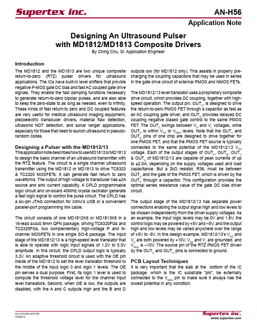
Supertex inc.AN-H56Application NoteIntroductionThe MD1812 and the MD1813 are two unique composite return-to-zero (RTZ) pulser drivers for ultrasound applications. The ICs have built-in level shifters that provide negative P-MOS gate DC bias and fast AC coupled gate drivesignals. They enable the fast damping functions necessary to generate return-to-zero bipolar pulses, and are also able to keep the zero-state to as long as needed, even to infinity. These kinds of fast return-to zero and DC coupled features are very useful for medical ultrasound imaging equipment, piezoelectric transducer drivers, material flaw detection, ultrasonic NDT detection, and sonar ranger applications, especially for those that need to launch ultrasound in pseudo-random codes. Designing a Pulser with the MD1812/13This a pplication n ote d escribes h ow t o u se M D1812 o r M D1813 to design the basic channel of an ultrasound transmitter with the RTZ feature. The circuit is a single channel ultrasound transmitter using the MD1812 or MD1813 to drive TC6320 & TC2320 MOSFETs. It can generate fast return to zero waveforms. The output of high voltage to transducer has ±2A source and sink current capability. A CPLD programmable logic circuit and on-board 40MHz crystal oscillator generate a fast logic signal to control the pulse circuit. The CPLD hasa six-pin JTAG connection for Xilinx’s USB or a convenient parallel-port programming link cable. The circuit consists of one MD1812K6 or MD1813K6 in a 16-lead 4x4x0.9mm QFN package, driving TC6320FGs and TC2320FGs, two complementary high-voltage P and N- channel MOSFETs in one single SO-8 package. The input stage of the MD1812/13 is a high-speed level translator that is able to operate with logic input signals of 1.2V to 5.0V amplitude. In this circuit, the CPLD output logic is typically 3.3V. An adaptive threshold circuit is used with the OE pininside of the MD1812 to set the level translator threshold to the middle of the input logic 0 and logic 1 levels. The OE pin serves a dual purpose. First, its logic 1 level is used to compute the threshold voltage level for the channel input level translators. Second, when OE is low, the outputs are disabled, with the A and C outputs high and the B and Doutputs low (for MD1812 only). This assists in properly pre-charging the coupling capacitors that may be used in series in the gate drive circuit of external PMOS and NMOS FETs. The MD1812/13 level translator uses a proprietary composite drive circuit, which provides DC coupling, together with high-speed operation. The output pin, OUT C , is designed to drive the return-to-zero PMOS FET through a capacitor as fast as an AC coupling gate driver, and OUT G provides delayed DC coupling negative biased gate control to the same PMOS FET. The OUT C swings between V H and V L voltages, while OUT G is within V SS or V NEG levels. Note that the OUT C and OUT G pins of one chip are designed to drive together forone PMOS FET, and that the PMOS FET source is typicallyconnected to the same potential of the MD1812/13 V SS voltage. Each of the output stages of OUT A , OUT B , OUT C & OUT D of MD1812/13 are capable of peak currents of up to ±2.0A, depending on the supply voltages used and load capacitance. But a 2kΩ resistor, R36, must be between OUT G and the gate of the PMOS FET, which is driven by the OUT C through a capacitor. This configuration provides the optimal series resistance value of the gate DC bias driver circuit.The output stage of the MD1812/13 has separate power connections enabling the output signal high and low levels to be chosen independently from the driver supply voltages. As an example, the input logic levels may be 0V and 1.8V, the control logic may be powered by +5V and –5V, and the output high and low levels may be varied anywhere over the range of +5V to -5V. In this design example, MD1812/13’s V DD and V H are both powered by +10V, V SS and V L are grounded, and V NEG is –10V. The source pin of the RTZ PMOS FET driven by the OUT C and OUT G pins is connected to ground.PCB Layout TechniquesIt is very important that the slab at the bottom of the IC package, which is the IC substrate “pin”, be externally connected to the V NEG pin to make sure it always has the lowest potential in any condition.Designing An Ultrasound Pulser with MD1812/MD1813 Composite DriversBy Ching Chu, Sr. Application EngineerUse high-speed PCB trace design practices that are compatible with the circuit’s operating speed. The internal circuitry of the MD1812/13 can operate at up to 100MHz, with the primary speed limitation being due to load capacitance. Because of this high speed and the high transient currents that result when driving capacitive loads, the supply voltage bypass capacitors should be as close to the supply pins as possible. The V SS and V L pins should have low inductance feed-through connections that are connected directly to a solid ground plane. If these voltages are not zero, they will require bypass capacitors similar to the positive power supplies. The V DD and V H supplies determine the output logic levels. These two pins can draw fast transient currents of up to 2.0A, so they should be provided with a low-impedance bypass capacitor at the chip’s pins. A ceramic capacitor of up to 1.0µF may be appropriate. Minimize the trace length to the ground plane, and insert a ferrite bead in the power supply lead to the capacitor to prevent resonance in the power supply lines. A common voltage source and local decoupling capacitor may be used for the V DD and V H pins, which should always have the same DC level applied to them. For applications that are sensitive to jitter and noise, insert another ferrite bead between V DD and V H and decouple each pin separately.Pay particular attention to minimizing trace lengths and using sufficient trace width to reduce inductance. Surfacemount components are highly recommended. Since the output impedance of this driver is very low, in some cases it may be desirable to add a small value resistor in series with the output to obtain better waveform integrity at the load terminals. This will, of course, reduce the output voltage slew rate at the terminals of a capacitive load. Pay particular attention to the parasitic coupling from the driver’s output to the input signal terminals. This feedback may causeoscillations or spurious waveform shapes on the edges of signal transitions. Since the input operates with signals down to 1.2V, even small coupling voltages may cause problems. Use of a solid ground plane and good power and signal layout practices will prevent this problem. Also ensure that the circulating ground return current from a capacitive load cannot react with common inductance to create noise voltages in the input logic circuitry.Testing the Ultrasound Pulser The MD1812 RTZ pulser design example is tested with the following power supply voltage and current limiting: V PP 0 to +100V 5mA, V NN 0 to -100V 5mA, V DD = +10V 50mA, V NEG -10V 5mA, V CC +3.3V, 90mA.The HV OUT signal appears at the SMA connector J6. There is a 5:1 attenuation of the signal, due to the value of resistor R11. When driving a real transducer load, the value of this resistor should be reduced in value to match the load impedance.The HV OUT signal passes through jumper J5, which can be used to terminate the HV OUT signal in a dummy load, comprising a 220pF capacitor in parallel with a 1kΩ resistor. When an external load is connected, the dummy load is not required, and J5 can be configured to pass the signals straight through to the output connector J6.All the on-board test points are designed to work with an active oscilloscope probe, such as the Tektronix P6243 1MΩ active probe. Because TP7 is connected to the HV OUT , where potentially damaging voltages could be present, make sure that V PP /V NN does not exceed the probe limit. If using another type of high impedance oscilloscope probe for the test points, ensure that the ground lead connections to the circuit board ground plane are as short as possible.There are multiple frequency and waveform combinations that can be selected as bipolar pulses, PW or CW waveforms. An external clock input can be used if the on-board 40MHz-oscillator is disabled. The external trigger input can be used to synchronize the output waveforms. There are five push buttons for selecting demo waveform, frequency, phase, and MD1812 chip enable functions. Color LEDs indicate the demo selection states. The CH1 output allows the monitoring of one of the 5 inputs (IN A , IN B , IN C , IN D or O E ) of the MD1812/13 via the select button. The MD1812 and the MD1813 are very similar in function. The only differences between them are the control of the OE (MD1812) vs VLL (MD1813) pin and their logic functions. Please read their data sheets for the details. In this design example, the CPLD program is using an on-board solder jumper, R34, to sense the difference and works accordingly. The example MD1812/13 pulser circuit schematic, detailsignals definitions, and some measured waveforms areshown below.Waveform C, 20MHz, 8 cycles Load: 220pF//1kPulser Circuit SchematicWaveform AWaveform CWaveform BWaveform DOE INA INB INC INDHV OUTV PPV NNOE INA INB INC INDHV OUTV PPV NNOE INAINBINC INDHV OUTV PPV NNOEINAINBINC IND HV OUTV PPV NNNote: The duty cycle of the PW burst is set about 0.2% for limitedpower dissipationNote: The duty cycle of the PW burst is set about 25% at ≤5.0MHz forlimited power dissipation.AN-H56MD1812/13 Reference DesignJ 6X D C RJ E X = L oFig. 1 Waveform of 2.5MHz Fig. 2 Waveform of 5MHzFig. 3 Waveform of 10MHz Fig. 4 Waveform of 10MHz InvertingFig. 5 Waveform of 20MHz 8 Cycles Fig. 6 Waveform of 5mHz & Delay ReadingsFig. 7 Waveform of 10MHz(at IN C , OUT C , OUT G , and P- Gate, V DD = 12V, V NEG = -10V)Fig. 8 Waveform of 5MHz(at IN C , OUT C , OUT G , and P- Gate, V DD = 5V, V NEG = -10V)Supertex inc. does not recommend the use of its products in life support applications, and will not knowingly sell them for use in such applications unless it receives an adequate “product liability indemnification insurance agreement.” Supertex inc. does not assume responsibility for use of devices described, and limits its liability to the replacement of the devices determined defective due to workmanship. No responsibility is assumed for possible omissions and inaccuracies. Circuitry and specifications are subject to change without notice. For the latest product specifications refer to the Supertex inc. (website: http//)©2013 Supertex inc.All rights reserved. Unauthorized use or reproduction is prohibited.Supertex inc.。
Xitanium FULL Prog LED Xtreme 驱动器数据手册说明书

Xitanium FULL Prog LED Xtreme driversXi FP 75W 0.3-1.0A SNLDAE 230V S240 sXt9290 021 28506Xitanium FULL Prog LED Xtreme driversPhilips Xitanium Full Programmable LED drivers are specifically designed to deliver the highest performance, protection and configurability.The portfolio offers both central and standalone dimming protocols further increasing the energy savings and CO 2 reductions achieved with LED lighting. The Xtreme technology ensures maximum robustness and protection combined with a very long lifetime.In this product family Philips introduces new drivers in a compact form factor with state-of-the-art features, which offer high value for both OEM customers and end-users. The products can replace the existing programmable outdoor LED drivers and will bring significant improvement in programming, assembly into a luminaire and electrical performance. Benefits•Ultimate robustness, offering peace of mind and lower maintenance costs•Fully programmable LED-drivers designed for the new digital and connected lighting world •Extended diagnostics via MultiOne•Easy to design-in, configure and install for Class I and Class II applications•Energy savings through high efficiency and via multiple dimming optionsFeatures•High surge protection (CM/DM)•Long lifetime and robust protection against moisture, vibration and temperature •Configurable operating windows (AOC)•Multiple control interfaces: DALI, AmpDim, 1-step and 3-step LineSwitch •Autonomous dimming via integrated DynaDimmer•Adjustable thermal protection for driver (DTL) and LED module (MTP)•Constant Light Output (CLO)•Adjustable Start-up Time (AST)•Adjustable Light Output (ALO)•End-Of-Life indicator (EOL)•Communication through mains via coded commands •Compliant per DALI Part 251/252/253 (select models)Application•Road and street lighting•Area lighting •Tunnel lighting•Industrial lighting April 2023Logistical dataSpecification item ValueProduct name Xi FP 75W 0.3-1.0A SNLDAE 230V S240 sXtEOC871869970573200Logistic code 12NC9290 021 28506EAN1 (GTIN)8718699705732EAN3 (box)8718699705749Pieces per box10Electrical input dataSpecification item Value Unit ConditionRated input voltage range202...254V ac Performance rangeRated input voltage230V acRated input frequency range47...63Hz Performance rangeRated input current0.36A@ rated output power @ rated input voltageMax. input current0.43A@ rated output power @ minimum performance input voltage Rated input power82W@ rated output power @ rated input voltageMinimum Power factor0.99@ rated output power @ rated input voltageTotal harmonic distortion7.5%@ rated output power @ rated input voltageEfficiency90%@ratedoutputpower@************************** Rated input voltage DC range186...250V dc Performance range, no external DC-rated fuse required Rated input current DC range0.3A dc Performance rangeInput voltage AC range80...264V ac Safety operational range, see MainsGuard graphInput frequency AC range45...66Hz Safety operational rangeInput voltage DC range168...275V dc Safety operational rangeStandby Power (no load)0.45WIsolation input to output DoubleElectrical output dataSpecification item Value Unit ConditionRegulation method Constant CurrentOutput voltage35...108V dcOutput voltage max.140V Maximum voltage at open loadOutput current0.07...1.05AOutput current min programmable300mAMin output current70mAOutput current tolerance ±3%@full loadOutput current ripple LF≤ 4%Ripple = peak / average @ < 3kHzOutput current ripple HF≤ 4%Output P st LM≤ 0.36In entire operating windowOutput SVM≤ 0.07In entire operating windowOutput power 2.5...75WElectrical data controls inputSpecification itemValueUnit ConditionControl methodAmpDim, Coded Mains, DALI,Dynadimmer, LineSwitch 3-step,LineSwitch single-stepOutput current amplitude dimming. Please refer to design-in guide at /oem for more controllability details.Dimming range 10...100%For latest DALI certification status please visit/products; LineSwitch: Vlow:< 160Vac Vhigh: 170 ... 264VacIsolation controls input to output Double acc. IEC61347-1Wiring and ConnectionsSpecification itemValueUnitTypeInput wire cross-section 0.2...1.5 / 24...16mm 2 / AWG solid / stranded wireInput wire strip length 8.5...9.5mm Output wire cross-section 0.2...1.5 / 24...16mm 2 / AWG solid / stranded wireOutput wire strip length 8.5...9.5mm Control wire cross-section 0.2...1.5 / 24...16mm 2 / AWG solid / stranded wireControl wire strip length 8.5...9.5mm Maximum cable length2.5m CISPR15: between driver and LED moduleMaximum NTC output cable length0.6mIsolationInsulation per IEC61347-1Mains + LineSwitchEQUILED + NTCDALIMains + LineSwitch -Double Double Basic EQUI Double -Basic Double LED + NTC Double Basic -Double DALIBasicDoubleDouble-Dimensions and weightSpecification item Value Unit Tolerance (mm)Length (A1)240.5mmMounting hole distance (A2)226.2mmWidth (B1)58.6mmWidth (B2)42.9mmHeight (C1)37.8mmMounting hole diameter (D1) 4.5mmWeight600gramOperational temperatures and humiditySpecification item Value Unit ConditionAmbient temperature-40...+55ºC Higher ambient temperature allowed as long as Tcase-max is notexceededTcase-max85ºC Maximum temperature measured at T case-pointTcase-life75ºC Measured at T case-pointMaximum housing temperature130ºC In case of a failure, inherent by designRelative humidity10...90%Non-condensingLifetimeSpecification item Value Unit ConditionDriver lifetime100,000hours Measured temperature at Tcase-point is Tcase-life. Maximumfailures = 10%Storage temperature and humiditySpecification item Value Unit ConditionAmbient temperature-40...+85ºCRelative humidity 5...95%Non-condensingProgrammable featuresSpecification item Available Default setting ConditionSet Adjustable Output Current (AOC)Programmable, SimpleSet700 mALED Module Temperature Protection (MTP)Yes OFFDriver Temperature Limit (DTL)Yes ONAdjustable Light Output (ALO)Yes OFFConstant Light Output (CLO)Yes OFFAdjustable Start-up Time (AST)Yes 1 sIntegrated Dynadimmer Yes OFF5-step, light turn-off possibleLineSwitch single-step Yes ONLineSwitch 3-step Yes OFFAmpDim Yes OFFMin Dim Level Yes10 %DC emergency (DCemDim)Yes ON Default: AOC = 15%. EOFx = 10 ... 60%. No external DC rated fuserequired. Internal fuse rating: T6.3A 250VAC/DC.End Of Life indicator (EOL)Yes OFFCoded Mains Yes OFFOEM Write Protection (OWP)Yes OFFDiagnostics Yes —FeaturesSpecification item Value ConditionOpen load protection Yes Automatic recoveringShort circuit protection Yes Automatic recoveringOver power protection Yes Automatic recoveringHot wiring NoSuitable for fixtures with protection class I and II per IEC60598Overtemperature protection Yes Automatic recoveringInrush currentSpecification item Value Unit ConditionInrush current55A Input voltage 230VInrush peak width200µs Input voltage 230 V, measured at 50% heightDrivers / MCB 16A type B≤ 11pcs Indicative value at 230VPlease refer to the driver design in guide if you use other MCB-types.If several mini circuit breakers are used directly side-by-side (without distance pieces)a correction factor of 80% has to be applied to the rated currentDriver touch current / protective conductor current / earth leakage currentSpecification item Value Unit ConditionTypical Touch Current (ins. Class II)0.3mA peak Acc. IEC61347-1. LED module contribution not includedTypical Protective Conductor Current (ins. Class I)0.18mA rms Acc. IEC60598-1. LED module contribution not includedSurge immunitySpecification item Value Unit ConditionMains surge immunity (diff. mode)6kV L-N, Ls-L, Ls-N, acc. IEC61000-4-5. 2 Ohm, 1.2/50us, 8/20us Mains surge immunity (comm. mode)10kV L/N/Ls - EQUI 10kV acc. EN61547; 8kV acc. IEC61000-4-5, 12 Ohm1.2/50us,8/20usControl surge immunity (diff. mode)0.9kV DALI - DALI, acc. IEC61000-4-5. 2 Ohm, 1.2/50us, 8/20us Control surge immunity (comm. mode)6kV DALI - EQUI acc. IEC61000-4-5. 12 Ohm, 1.2/50us, 8/20us Control surge immunity (comm. mode)8kV DALI - L/N/Ls acc. IEC61000-4-5. 12 Ohm, 1.2/50us, 8/20usApplication InfoSpecification item ValueApproval marks and Certifications CCC / CE / DALI 2 / Double-insulated Built-In / EAC / EL / ENEC / RCM / TISI / UA / UKCA / WEEEIngress Protection classification (IP)20Application OutdoorMounting Type Built-inGraphs Operating windowThermal GuardMains GuardPower factor versus output powerEfficiency versus output powerTHD versus output power©2023 Signify Holding, IBRS 10461, 5600 VB, NL. All rights reserved.UK importer address: Signify Commercial UK Limited, 3, Guildford Business Park, GU2 8XG.The information provided herein is subject to change without notice. Signify does not give any representation or warranty as to the accuracy or completeness of the information included herein and shall not be liable for any action in reliance thereon. The information presented in this document is not intended as any commercial offer and does not form part of any quotation or contract, unless otherwise agreed by Signify.Philips and the Philips Shield Emblem are registered trademarks of Koninklijke Philips N.V. All other trademarks are owned by Signify Holding or their respective owners.Date of release: April 13, 2023 v4/oem。
印能捷Connect工作流程系统(版本5.0)Workshop用户指南简体中文(下册)
在最终输出中保留专色
785
目标
选择此选项
保留一个专色
分离
(只有在处理模板的输出转换部分选择了制作色 版复选框, 该色版才会分色输出。)
在打样中忽略一个 颜色
不要输出
c. 单击确定。
3. 通过将选定的印面或帖拖到拼版输出处理模板,对这些印面或帖 开始拼版输出处理。
4. 通过设置处理模板中的一个选项而保留所有其他专色: a. 在开始处理对话框中,单击编辑处理模板。 b. 展开输出转换部分。 c. 在输出分色处理列表中,选择全部分色输出。 d. 关闭该处理模板。
关于无专色扩展颜色管理
791
输出 输出
输出
列出已在页面颜色 列表中对每种颜色指定的颜色输出处理 办法。
选择输出为
指定希望 Prinergy 如何输出每个颜色。在页面颜色栏中选 择一种或多种颜色后,列表会显示以下选项: ● 分离
输出专色。对于最终输出,Prinergy 会将专色作为分色 输出。对于拼版输出,如果在输出分色处理框中选择 输出所有分色,印能捷会将专色作为分色输出。
b. 选择专色,然后在选择输出为列表中选择一个选项:
要完成此操作
选择此选项
将一个专色转换为印 刷色
转成印刷色或一个印刷色
将一个专色映射为另 一个颜色
专色或印刷色
(如果该颜色已经不存在,首先添加一个分 色。)
788
第 13 章 -颜色
要完成此操作 保留颜色
选择此选项
分离 (只有在处理模板的输出转换部分选择了制作 色版复选框,该色版才会分色输出。)
3. 通过清除处理模板中的一个选项而保留专色: a. 在开始处理对话框中,单击编辑处理模板。 b. 展开输出转换部分或颜色转换部分。 c. 在颜色库区域中,清除始终使用颜色组合器来转换专色复选 框。 d. 关闭该处理模板。
各大LED驱动芯片大全

不知道发过没?各大LED驱动芯片大全Fairchild (美国飞兆) FSEZ 1016主要应用于3W灯杯3WFSEZ 1216主要应用于5W灯杯5WFSQ 110主要应用于8W左右LED电源8WFSDH 321主要应用于8W左右LED电源8WKA5M02659RN主要应用于12W左右LED电源12WKA5M0365R/KA5M0380RYDTU主要应用于30W左右LED电源30WFSDL0165/FSDM0265/FSDM0365 主要应用于12-18WLED电源12-18WKA5L0365RN/KA5M0365RN主要应用于24WLED电源25WSG6859 + 2N60/4N60主要应用于日光灯等外置式LED电源30W 以下SG6741 + 7N60C/7N60C主要应用于日光灯等外置式LED电源60W 以下FSFR2100主要应用于LED路灯和大功率LED电源200W待补充Power Integrations (PI) LNK603/613PG/DG主要应用于2.5W的LED灯杯2.5WLNK604/614PG/DG主要应用于3.5W的LED灯杯3.5WLNK605/615PG/DG主要应用于4.5W的LED灯杯4.5WLNK606/616PG/GG主要应用于5.5W的LED灯杯5.5WTNY274/275/276/277P/G主要应用于5-8W LED电源5-8WTNY278/279/280P/G主要应用于10-14W LED电源10-14W待补充Supertex (美国超科) AT9933专为汽车设计用高达70V功率驱动ICHV9921/22/2385 to 264V AC or DC input voltage of 20 to400V. 20/30/50mAHV9925Output Current to 50mA;Universal 85-264V AC Operation;Fixed OFF-Time BuckConverter;Internal 500V Power MOSFETHV9903Power efficiency of up to 85%;Drives up to 6 White LEDs;2.6V to 4.6VSupply;power stage can operate at 1.8V;Built-in Soft Start;DC and PWM DimmingControlHV9910高压大功率直驱LED恒流器件HV9911高压双向检测大功率直驱LED恒流ICHV9931高压双向检测大功率直驱LED恒流IC,可PWM灰度调节待补充National (美国国半) 针对带有双电流槽和与IC兼容亮度控制的白色LED和QLED显示器的高效升压器LM3402针对高功率LED驱动器、6V至42V输入电压范围的0.5A持续电流降压电路LM3402HV 针对高功率LED驱动器,6V至75V输入电压范围的0.5A持续电流降压电路LM3404针对高功率LED驱动器,6V至42V输入电压范围的1A持续电流降压电路LM3404HV 针对高功率LED驱动器、6V至75V输入电压范围的1.0A持续电流降压电路LM5022针对升压和SEPIC稳压器的60V低压侧控制器,允许控制外部MOSFET来为LED提供LM2735 520kHz/1.6MHz - 有效使用空间的升压和SEPIC DC-DC稳压器LM3405用于LED驱动器500kHz/1.6MHz 1A恒流降压稳压器LM2754具有超时保护功能的800mA开关电容Flash LED驱动器LM27965具有I2C兼容亮度控制功能的双显示器白光LED驱动器LM27966带有I2C兼容接口的白光LED驱动器LM2727/ LM2737 频道的FET 同步的为低输出电压顽强反抗调整者控制器待补充美国国家半导体公司白色LED低功率驱动部分LM3519高的频率推进白色LED用高速的PWM 光亮控制驱动ICLM2731SOT23 小封装小功率LED驱动应用SOT23 小封装5V升压到12-30V,120-300mALM26238-14V 转换成输出电压在1.24-14V之间,达到90% 的效率LM3557为白色LED2.7V-7.5V的递升转换器,多大5颗LED小体积背光指示LM35022.5-5.5V升压到16-44V,多达4-10颗LED小体积背光指示LM27512 X,1.5 X 电容器式倍压白色LED的引导驱动ICLM3590系列小功率白色LED简单驱动,降压型LM2707系列小功率白色LED简单驱动,升压型LM35082.7Vto5.5V 升压17.5V 驱动4个白色LED达到30mA 应用ICLM2793白色的低噪音引2.5-5.5V,1.5倍压双重的功能光亮控制ICLM2792接受输入电压从3.0V到5.8V的范围和维持持续的电容器类光亮控制LM2791受输入电压从3V到5.8V的范围和维持持续的36mA由外部的固定电阻决定. LM2705直流的升压式150mA的直流转换器LM2703直流的升压式350mA的直流转换器LM3501同时的递升直流/ 直流转换器为白色LED的驱动LM2794/LM2795 多路驱动补给的电容器类比和PWM 灰度控制LM27953 白色LED四路的和3/2 x转变了电容器推进式驱动LM3570低的噪音白色LED,应用与手持式设备多路控制多颗LED背光指示LM3595 平行的白色LED驱动应用LM2704 2.2-7V升压20V,550mA,SOT小封装LED驱动LM2750 低的噪音转变了电容器小功率升压驱动LM2796 双重的3/2 x 的白色LED驱动电容器式应用ICLM27964 有I2C 的独立控制的,多按键区域背光指示应用ICLM2756有I2C 的独立控制的,多按键区域背光指示应用ICLM2754带有超时保护功能的800mA开关电容器Flash LED驱动器LM3551/LM35521A白色用闪光灯驱动应用LM3224直流的递升PWM 的615 KHz/1.25 MHz/直流转换器待补充美国国家半导体公司照明管理单元(LMU)LM4970声音同步化LED驱动器IC适合任何颜色LP3943RGB/白色/ 蓝色16通道引导的LED驱动器LP3944RGB/白色/ 蓝色8 通道引导的LEDLP5520RGB背光LED驱动器LP5521可编程的三通道LED 驱动器LP5522可编程的LED驱动器LP3958高电压推进的照明管理转换器LED应用ICLP5526高的电压推进的照明管理可达到150mA序列闪光的驱动ICLP3936为六白色的照明管理系统引导和一RGB 或闪光引导LP3931双路的RGB 用高亮度驱动DC-DC转换器LP3933为六白色的照明管理系统应用和二RGB 或闪光应用ICLP3954电话LED指示包括展览背光、RGB、按键区和照相机闪光等应用LP3950颜色用声音的同步装置引导LED驱动LP39526个通道的颜色用声音的同步引导驱动应用ICLP39542多路LED背光管理ICLP55281四路RGB驱动器LP5527为照相机闪光的极小驱动和4以I2C应用Programmability,连接性测试和声音LP55271为照相机闪光的极小驱动和4以I2C应用Programmability,连接性测试和声音待补充International Rectifier (IR) IRS2540S/2540PBF一款高压,高频降压调节控制集成电路,该产品用于要求多个LED的交流-直流离线,非隔离应用电路或要求直流-直流混合色能力的应用.应用包括室内外标牌,以及建筑,娱乐,设计和装饰照明.IRS2541S/2541PBF一款高压,高频降压调节控制集成电路,该产品用于要求多个LED的交流-直流离线,非隔离应用电路或要求直流-直流混合色能力的应用.应用包括室内外标牌,以及建筑,娱乐,设计和装饰照明.待补充Nxp (恩智浦) LED屏幕配套部分逻辑IC,飞利浦系列:74HC595D逻辑8位移位寄存器74HC245D3态8总线收发器74HC138D3-8线译码器、多路转换74HC164D8位移位寄存器(串进并出)74HC04D逻辑6非门74HC08D逻辑6非门驱动器74HC244D8缓冲/线驱动/线接收(3态)待补充Maxim-Dallas (美国美信) 美国美信高亮度LED驱动器部分MAX16800高电压6.5-40V驱动35-350mA多颗LED应用驱动ICMAX16801A/BPWM 控制器265V AC-85V AC1A LED驱动器MAX16802A/BPWM 控制器10.8VDC-24VDC 1A LED驱动器MAX16803 高压、350mA、高亮度LED驱动器, 提供PWM亮度调节和5V稳压器MAX16804 高电压5.5V-40V,350mA驱动和PWM 控制暗淡MAX16805/MAX16806 EEPROM可设计的,高电压,350mA台灯等现场调光驱动应用MAX16807/MAX16808 集成8通道LED驱动器,具有开关模式boost及SEPIC控制器MAX16809/MAX16810 集成16通道LED驱动器,具有开关模式boost及SEPIC控制器MAX168181.5 MHz,30A高效率LED恒流驱动MAX16819/MAX168202MHz高光亮LED驱动和5000:1灰度等级调节MAX16823高电压4.5-40V,3通道独立,5mA到70mA和外接BJT时可达到2AMAX16824/MAX16825 3通道、高亮度LED (HB LED)驱动器,6.5V至28V输入电压MAX7302低电压LED驱动器,提供闪烁控制、PWM调节、瞬变检测及电平转换待补充美国美信白光LED驱动器部分MAX8678白光LED在喇叭上整合应用ICMAX1698,MAX1698A便携式LCD屏背光源白光LED驱动应用ICMAX1848手机等小屏锂电池单色LED背光源恒流驱动ICMAX1916小体低压差式恒流驱动ICMAX1910/MAX1912锂电池1.5x/2x倍压式LED驱动器,最大120mAMAX1570锂电池1x/1.5x 倍压式LED驱动器,多路可PWM调光MAX1984/MAX1985/MAX1986白色LED超高效率恒流驱动MAX1582/MAX1582Y可编程升压型2段恒流驱动ICMAX1553/MAX1554高效率, 升压到40V为2 到10 白色LED的转换器驱动MAX1573白色泵式1 x/1.5 x驱动器,小体积QFN型封装MAX1561/MAX1599高效率,升压型转换器26V驱动2到6颗白色LED驱动MAX1574180mA,1x/2x倍压白色泵式驱动IC 3毫米x3毫米TDFN小封装MAX1583白色的引导照相机-闪光推进转换器MAX1575白色LED驱动1x/1.5x电荷泵式光源指示MAX1576480mA白色LED1x/1.5x/2x电荷泵式从背光照亮到照相机闪光灯应用MAX1578/MAX1579TFT屏与LED背光整合驱动应用ICMAX8595Z/MAX8596Z高效率,2.6-5.5V升压型32V,25mA,2-8颗LED驱动应用MAX1577Y/MAX1577Z1.2 A 白色LED闪光灯应用ICMAX8630W/MAX8630X125mA 1x/1.5x电荷泵式为5颗白色LED小型TDFN封装MAX8631X/YLED电荷泵式1x/1.5x/2x4毫米x 4毫米的二LDOs使QFN超薄封装MAX8790六线白色LED恒流驱动,适合笔记本等中尺寸LCD背光MAX8607为1.5A的1MHz PWM 推进转换器白色LED应用照相机闪光MAX8647/MAX8648 超高效率电荷泵式6LED的/ RGB驱动应用,瘦小的QFN封装待补充ONSEMI (美**森美) NCP56122通道泵式可PWM的白色LED驱动产品是LCD屏背光照明,操作模态1 x 和1.5 x 泵式驱动,87% 效率连同0.2% 相配误差.NCP5623带I2C控制的三路输出RGB LED驱动器,完全支持RGB照明或白光LED背光,内置”渐进调光”功能,能效高达94%的电荷泵,具备1x和2x两种工作模式,采用节省空间的极小型LLGA-12 2.0×2.0×0.5 mm封装NCP3065, NCV3065输出1.5 A ,输入电压 3.0 V to 40 V, PWM灰度调节,为汽车应用设计NCP5007小型小体2.7 to5.5 V 升压驱动多颗LED,小屏背光及背光指示等应用NCP5008,NCP50092.7 到6.0 V 输入电压范围,从Vbat 到15 V 的输出电压,外设光敏电阻NCP5010: Integrated Backlight LED BoostDriverNCP5030: Buck-Boost Converter to Drive aSingle LED from 1 Li-Ion or 3 Alkaline BatteriesNCP5604A, NCP5604BHigh Efficiency White LEDDriverNCP5603: High Efficiency Charge PumpConverter / White LED DriverNCP5602: 2-Channel Charge Pump White LEDDriver with I²C ControlNUD4001AC−DC 输入5.0 V, 12 V or 24 V.输出最大500mA,最简易型LED驱动ICNUD4011AC−DC 输入最大120 V.输出最大70mA,最简易型多颗LED驱动ICZetex (英国ZETEX ) ZXLB1600 LED/OLED 升压偏置1.6 - 5.5 28 75 350 MSOP10ZXLD1100 LED 升压驱动器2.5 - 5.5 28V(最大) 60 350 SC70-6ZXLD1101 LED 升压驱动器2.5 - 5.5 28V(最大) 60 350 TSOT23-5ZXLD1320 内置开关式1.5A LED 驱动器4 至18 18 122000 TDFN1433 ZXLD1321 内置开关式1A LED 驱动器1.2 至12 18 122000 TDFN1433 ZXLD1322 内置开关式0.7A LED 驱动器2.5 至15 18 122000 DFN1433 ZXLD1350 内置开关式350mA LED 驱动器7 至30 30 15 370TSOT23-5 ZXLD1360 内置开关式1A LED 驱动器7 至30 30 201000 TSOT23-5 ZXLD1362 内置开关式1A LED 驱动器6 至60 60 651000 TSOT23-5 ZXLD1575 x1/x1.5 充电泵6 通道驱动器2.7 至5.5 5.5 1000120 QFN1644 ZXLD1601 LCD/OLED 升压偏置2.5 - 5.5 VIN 至28 60 320 SC70-6ZXLD1615 LCD/OLED 升压偏置2.5 - 5.5 VIN 至28 60 320 TSOT23-5 ZXLD1937 LED 升压驱动器2.5 - 5.5 28V(最大) 60 350 TSOT23-5ZXSC300 LED 升压/降压驱动器0.8 -8.0 Vin 至Vm 200 外置开关SOT23-5 ZXSC310 LED 升压/降压驱动器0.8 -8.0 Vin 至Vm 200 外置开关SOT23-5 ZXSC380 内置开关式单室简易升压0.8 - 6.0 Vin 至20V 80 - SOT23ZXSC400 LED 升压驱动器1.8 - 8.0 Vin 至Vm 150 外置开关SOT23-6 ZXSC440 相机闪光灯驱动器1.8 - 8.0 Vin 至Vm 150 外置开关MSOP8待补充Texas Instruments (TI) TI 美国德州仪器公司屏幕驱动部分TLC59048/16 通道LED 驱动器TLC59058/16 通道LED 驱动器TLC591116 通道LED 驱动器TLC5916/TLC59178通道LED驱动器TLC592016 通道LED 驱动器TLC592116 通道LED 驱动器TLC5922带有点校正的16 通道LED 驱动器TLC5923带有点校正的16 通道LED 驱动器TLC5924具有点校正功能和预充电FET 的16 通道LED 驱动器TLC593012 通道LED 驱动器TLC5940带有EEprom 点校正与灰度PWM 控制的16 通道LED 驱动器TLC5941带有点校正与灰度PWM 控制的16 通道LED 驱动器TLC5945带有点校正、灰度PWM 控制和无延迟的16 通道LED 驱动器TI 美国德州仪器公司白光LED驱动器TPS60250具有I2C 接口的用于7 个WLED 的1.2A 高功率高效充电泵TPS60251具有I2C 接口的用于7 个WLED 的1.2A 高功率高效充电泵TPS60252同步推进转换器I2C/可并立的接口白色驱动器TPS6102*可调节、1.5A 开关、96% 高效升压转换器,具有降压模式TPS61040/41用于LCD 和白光LED 的,输入1.8-6V出28V 400mA 开关升压转换器TPS61042输入1.8-6V出30V 500mA 开关升压转换器,用于白光LED 应用领域TPS61043升压PWM灰度可调恒流LED驱动TPS6104528V 85% 效率的升压转换器,用于LCD 应用领域TPS61055具有I2C 兼容接口的 1.2A 高功率白光LED 驱动器TPS61058具有1.1A 开关的高功率单个白光LED 驱动器TPS61059具有1.5A 开关的高功率单个白光LED 驱动器TPS61060/TPS61061/TPS61062具有白光LED 亮度控制电源的15V、400mA 开关,1MHz 升压转换器TPS61080具有集成功率二极管的27V、500mA 开关、1.2MHz 升压转换器TPS61081具有集成功率二极管的27V、500mA 开关、1.2MHz 升压转换器TPS61140具有OLED和LCD背光屏双重驱动的应用ICTPS61141具有OLED和LCD背光屏双重驱动的应用ICTPS61150使用单一控制双输出LED驱动背光源驱动ICTPS61151使用单一控制双输出LED驱动背光源驱动ICTPS61150A使用单一控制双输出背光源驱动多大14颗LED能力的ICTPS61160PWM白光LED 2.7-18V升压500mA,最多6pcs LEDTPS61161PWM白光LED 2.7-18V升压500mA,最多10pcs LEDTPS61165PWM白光LED 3-18V升压1.2A,最多3pcs LEDTPS75103LDO低压差背光源LED驱动ICTPS75105LDO低压差背光源LED驱动ICTPS61180/1/25-24V输入多路25mA,最大10WLED背光驱动ICToshiba (日本东芝) TB627258位移位恒流驱动ICTB62726AN/AF16位全彩LED大屏幕TB62726ANG/AFG16位全彩LED大屏幕TCA62746AFG/AFNG16位全彩LED大屏幕带断、短路侦测及温度保护Siti (台湾点晶科技股份) DD311单信道大功率恒流驱动IC最大1A最高耐压36V线性恒流ICDD312单信道大功率恒流驱动IC最大1A最高耐压18V线性恒流ICDD313三信道大功率恒流驱动IC500mA R/G/B恒流驱动ICDM412三通道装饰照明专用可直接数据级联恒流IC 200mA R/G/B恒流驱动ICDM413三通道装饰照明专用PWM输出驱动IC 100mA R/G/B恒流驱动ICDM114,DM115新版8位驱动IC 主要是用于屏幕及灯饰DM115B通用8位恒流驱动IC 恒流一致性及稳定性高DM11A8位恒流动,用于护栏管,屏幕灯饰使用DM11C8位驱动IC 具有短断点侦测及温度保护功能,屏幕灯饰使用DM13C16位驱动IC 具有短断点侦测及温度保护功能,屏幕灯饰使用DM13A16位恒流驱动,面对低端屏幕客户DM134,DM135, DM13616位驱动IC 主要用于LED屏幕及护栏管DM13216位1024级PWM输出驱动ICDM13716位开,短路,过温智能侦测驱动ICDM13316位开路检测&64级电流调整&过温警示驱动ICDM1638x3信道4096级PWM驱动ICDM6214×3装饰照明专用PWM输出驱动恒流ICDM63112比特内置PWM+实时检测恒流驱动ICDM63216比特内置PWM+实时检测恒流驱动ICDM1638×3通道4096级PWM输出恒流驱动ICDM1648×3通道4096级PWM输出恒流驱动ICDD211二倍升压驱动IC 2-3.3V 最大升压100mA固定式恒流ICDD2313信道驱动IC 5-30mA 可设置小体上电即亮型ICDD2334信道驱动IC 5-30mA 可设置小体、可开关型ICDD2121.5-5.5V二倍升压最大400mA电流输出驱动单颗LED恒流ICPC112,PC1132.8-5V四倍升压驱动20mA小功率多颗LED恒流ICST2225A35输出信道之数字/字母LED驱动芯片Addtek (广鹏科技)A701、A702固定式5-30mA灯饰恒流A703120mA可开式6-50V降压型恒流ICA705220mA、2.7-12V固定降压型单路恒流ICA7065-40mA、5-50V/PWM多路可开关型恒流ICAMC711x固定式小电流灯饰应用AMC711x_E固定式小电流灯饰应用AMC71352-6V低压差固定式恒流驱动IC1颗LEDAMC71405-50V DC&DC 最大500mA电流可调,1颗或多颗LED驱动ICAMC71505-24V DC&DC 最大1.5A固定式,1-3颗LED驱动ICAMC7169LED保护ICMBI (台湾聚积科技) MBI18011路恒流驱动1.2A电流可设定PWM信号灰度调节MBI18022路恒流驱动360mA电流可两路单独设定PWM信号灰度调节MBI18044路恒流驱动240mA电流可设定PWM信号灰度调节MBI181616路恒流驱动电流可设定PWM信号灰度调节MBI5024面对低端客户16位LED屏幕、护栏灯管恒流驱动ICMBI502516位最大45mALED屏幕、护栏灯管恒流驱动ICMBI502616位最大90mA LED屏幕、护栏灯管恒流驱动ICMBI502816位最大90mA LED屏幕、护栏灯管恒流驱动IC,具电流增益功能MBI503016位内置PWM高灰阶LED恒流驱动ICMBI503116位内置PWM高灰阶LED恒流驱动IC,相对5030低端客户MBI5039MBI51688位LED屏幕、护栏灯管恒流驱动ICMBI60103位级联式LED灯饰屏幕,R/G/B单独电流可设置恒流驱动IC StarChips (晶錡科技) SCT202416位移位LED恒流驱动,适合目前LED大屏幕使用3-40mASCT202616位移位LED恒流驱动,适合目前LED大屏幕使用3-90mASCT221016位移位LED恒流驱动,适合LED大屏幕及插件护栏管使用3-120mASCT21108位移位LED恒流驱动IC,主要用于灯饰产品SCT251212位移位护栏管专用IC,3路OE灰度可以单独调节SCT20073路点光源驱动IC,可兼容MIB6010Shamrock (台湾芯瑞)SMD7333-40V电压输入,内置MOS管降压型驱动电流1ASMD7353-40V电压输入,降压型驱动电流700mA(可替代AMC7150)SMD736最高40V电压输入,内置MOS管降压型驱动电流3ASMD802市电直驱1A LED驱动IC(可替代HV9910)SMD911市电直驱IC,外置MOS LED隔离方案驱动ICSMD912市电隔离型直驱IC,外置MOS LED驱动ICOB (台湾昂宝) OB656380W PFC Module 400V 0.2ATM PFCOB6573300W PFC Module 400V 0.75A CCM PFCOB6561P36W LED Driver 24V 1.5ATM PFCTAC (台湾台创) TAC7135TAC7136TAC9920TAC5240TAC5241深圳市泉芯电子QX2706 背光恒流驱动2.7V~5.5V <=30V <=200mA <=85% SOT23-6QX2705 背光恒流驱动2.7V~5.5V <=30V <=200mA <=87% SOT23-5QX2703 背光恒流驱动2.7V~5.5V <=30V <=200mA <=87% SOT23-5QX7136 矿灯/手电筒驱动2.7V~6V- <=3A - SOT89-5QX7135 矿灯/手电筒驱动2.7V~6V- <=400mA - SOT-89-3 TO-252-2QX5234 三通道恒流驱动5.5V~17V <=17V <=200mA - SOP16 SSOP16 TSSOP16QX5238/9 背光恒流驱动2.7V~6V 2.7V~6V 15mA/20mA <=90% SOT23-6 MSOP-8QX2305 LED日光灯恒流驱动2V~400V - - <=90% SOP-8QX9910 LED日光灯恒流驱动2.5V~400V 2.5V~400V <=1A <=90% SOP-8QX5232B 太阳能草坪灯驱动1.2V~4V 1.2V~4V <=120mA <=90% DIP-8QX5251 太阳能草坪灯驱动0.9V~1.5V - <=300mA <=92% TO-94QX62726 LED显示屏恒流驱动4V~5.5V <=10V <=90mA - SSOP24-300-1.00 SSOP24-150-0.635QX5241 大功率低压恒流驱动5.5V~36V 5.5V~36V <=2A <=95% SOT23-6杭州士兰微电子SB1672616位恒流驱动全彩屏幕ICSC16722可级连、大电流输出的专用LED驱动电路SB42351350mA低压差白光固定式LED驱动芯片SB42510PWM控制、1A白光LED恒流芯片SA7525PFC功率因素控制技领半导体上海有限公司ACT34US-T SOT23-6 65kHz 7W 0.3WProduction ACT351HQ-T SIP-4 Adjustable 2W < 0.3WSampling ACT353HQ-T SIP-4 Adjustable 3W < 0.3WSampling ACT355HQ-T SIP-4 Adjustable 3.5W < 0.3WSampling ACT50UC-T SOT23-5 65kHz 18W 0.3WProduction ACT50DH DIP-8 65kHz 30W 0.3WProduction华润矽威科技(上海) PT4107通用18V~450V市电输入,高亮度LED驱动器.PT411530V/1.2A,高调光比LED恒流驱动器深圳市明微电子有限公司SM16130 LED驱动控制电路SM16128 LED驱动控制电路SM16126C 16位恒流LED驱动器SM16126B 16位恒流LED驱动器SM74HC595 LED显示驱动专用集成电路SM8061 高效节能功率因子校正芯片。
datasheet参数对照表
Sd42524 杭州士兰微
Y
Y Y
MP2483 MPS Y Y
Y
MP3386 MPS
6
4.5
4.5
36
55
25
1A
2.5A
280KHZ 固定频率 250khz-1300kh 1.25MHz or
z
625kHz
最高效率
模拟调光
PWM 调光
Y
TRAIC 调
光
电流精度
过流保护
OVP
y
SWP
温度保护
Y
集成度
■Medical and ■Medical and
■
Industrial
Industrial Architecture
Instrumentati Instrumentati
Detail
on
on
lighting
■Video
■Video
Projectors
Projectors
RoHS
RoHS
SOP-8L,
Y
Y
SSL2101 最大 可以支持 15W 的输出功率; SSL2102 最大 可以支持 25W 的输出功率;
Y
Y Y 内建 MOSFET
96% Y
±1%
Y Y 集成 LDMOS
特点描述 应用
Constant Current Boost
Controller for Driving High Power
) 最高频率
(kHz)
MIC3230/1/2 Micrel
6 45
Programmable switching frequency (MIC3230/1) or 400kHz fixed frequency operation (MIC3232)
超特克电子EL灯驱动器电路应用指南说明书
Supertex inc.AN-H63Application NoteHV857 EL Lamp Driver CircuitsThis application note presents six EL driver circuits utilizing the Supertex HV857 integrated circuit. They have been optimized for a variety of applications and may be used as is or used as a starting point in designing a circuit for a particular application.When constructing and testing one of the driver circuits listed below, keep in mind that results may differ from those given due to component tolerances and lamp characteristics. When making component changes, always remove supply voltage first. After making adjustments, bring up the supply voltage slowly (starting from the minimum required device input voltage) while monitoring input current. Excessive input current may be a good indication of connection errors or incorrect component values. A sharp rise in current usually indicates a saturated inductor. To avoid inductor saturation, use a higher current rated inductor or increase the conversion frequency by lowering the RSWresistor value.Notes:1. Lamp brightness can vary by type and manufacturer.V IN 3.0VV IN 1.5VON = 3.0V OFF = 0VV IN 3.0VON = 3.0V OFF = 0VV IN 3.0VSupertex inc. does not recommend the use of its products in life support applications, and will not knowingly sell them for use in such applications unless it receives an adequate “product liability indemnification insurance agreement.” Supertex inc. does not assume responsibility for use of devices described, and limits its liability to the replacement of the devices determined defective due to workmanship. No responsibility is assumed for possible omissions and inaccuracies. Circuitry and specifications are subject to change without notice. For the latest product specifications refer to the Supertex inc. (website: http//)©2013 Supertex inc. All rights reserved. Unauthorized use or reproduction is prohibited.Supertex inc.V IN 3.0VV IN 3.0V。
超图电子HV9861ADB1高光LED驱动板说明书
Supertex inc.HV9861ADB1General DescriptionThe HV9861ADB1 demoboard is a high-brightness LED driver employing the patented average-mode, constant current control scheme by Supertex Inc. The power conversion stage of the HV9861ADB1 consists of a diode bridge rectifier followed by a buck converter operating with fixed off-time of 20µs.The HV9861ADB1 LED driver features tight regulation of the LED current within a few milliamps over the entire range of the input AC line and the output LED string voltage. The LEDcurrent accuracy is almost insensitive to the passive component tolerances, such as the output filter inductance or the timing resistor. The accuracy of the LED current is mainly determined by the internal 270mV ± 3% reference voltage of the HV9861A control IC and by the external current sense resistor tolerance.(Note, that the linear dimming input of the HV9861A disables switching, when its voltage falls below a 200mV threshold.Expect the LED driver to shut off when the LED current falls below 50 ~ 55mA.)PWM dimming can be achieved by applying a pulse-width-modulated square wave signal between the PWMD and GND pins.The HV9861ADB1 features protection from an output short circuit condition. Open LED protection is inherent, since theoutput filter capacitor can accept the full rated rectified AC line voltage. Please, note that the demoboard is not CISPR15 compliant.An additional input EMI filter circuit is required to make the board meet conducted electro-magnetic emission limits. Also, note that:NO SAFETY ISOLATION OF THE LED LOAD FROM THE AC MAINS VOLTAGE IS PROVIDED!21-Watt, Universal, AC LED Driver Demoboard with Accurate Average-Mode, Constant Current ControlConnection Diagram WARNINGDo not connect earth-grounded test instruments. Doing so will short the AC line, resulting in damage to the instrument and/or the HV9861ADB1. Use floating high voltage differ -ential probes or isolate the demoboard by using an isolat-ing transformer.No galvanic isolation. Dangerous voltages are present when connected to the AC line.1. Connect the input AC voltage between the AC INterminals as shown in the connection diagram.2. Connect the LED string between LED+ (anode ofLED string) and LED- (cathode of LED string).3. Connect the PWMD terminal to the VDD terminalusing the jumper provided to enable the LED driver.4. The current level can be adjusted by applying 0 -1.5V between LD and GND. Leave LD floating to use the internal current setting.Connections90-265VAC50/60Hz0 -1.5V for LD function or leave openSilk ScreenPWM DimmingThe HV9861ADB1 is capable of being PWM dimmed by apply-ing a square wave TTL compatible signal between PWMD and GND terminals. However, since there is no galvanic isolation on the board, care must be taken to prevent damage to the PWM dimming source and/or the HV9861ADB1. One simple way is to isolate the LED driver from the AC line using an isola-tion transformer. Another approach is to use an opto-isolator to drive the PWMD pin as shown in the following figure.5.0Vsquarewavesignal(<1.0kHz)PWMDVDD(e.g. LTV-814 from Lite-On) Schematic60L E D C u r r e n t (A )AC Line Voltage (VAC)AC Line Voltage (VAC)L E D C u r r e n t (A )PWM Dimming Response Short Circuit CurrentI LEDPWMDV IN = 240VACTypical CharacteristicsSupertex inc. does not recommend the use of its products in life support applications, and will not knowingly sell them for use in such applications unless it receives an adequate “product liability indemnification insurance agreement.” Supertex inc. does not assume responsibility for use of devices described, and limits its liability to the replacement of the devices determined defective due to workmanship. No responsibility is assumed for possible omissions and inaccuracies. Circuitry and specifications are subject to change without notice. For the latest product specifications refer to the Supertex inc. (website: http//)©2013 Supertex inc.All rights reserved. Unauthorized use or reproduction is prohibited.Supertex inc.。
超特克(Supertex)高压DC DC转换器应用注解说明书
Supertex inc.AN-H59Application NoteApplication CircuitHigh Voltage DC/DC Converter forSupertex Ultrasound Transmitter DemoboardsBy Afshaneh Brown, Applications Engineer,and Jimes Lei, Applications ManagerIntroductionThe Supertex AN-H59DB1 demoboard is a high voltage DC/DC converter. It can provide up to +90V voltage supply for V PP and -90V for V NN . It also provides +8.0 to +10V voltage supply for V DD , floating power supplies of V NN +8.0 to V NN +10V for V NF and V PP -8.0 to V PP -10V for V PF . The input supply voltage is 12V.The AN-H59DB1 circuitry consists of two high voltage PWM Current-Mode controllers, a DC/DC transformer driver, and three low dropout regulators. The Supertex AN-H59DB1 uses a high-voltage, current mode, PWM controller boost topology to generate +15 to +90V and a high-voltage current mode PWM controller buck-boost topology to generate -15 to -90V power supply voltage for Supertex HV738DB1 and HV748DB1 ultrasound transmitter demoboards.Each of the transmitter demoboards has slightly different operating voltages as summarized below.To accommodate all three demoboards, the AN-H59DB1 demoboard has adjustable V PP , V NN , V DD , V PF and V NF . The purpose of the AN-H59DB1 is to aid in the evaluation of the three transmitter demoboards. The intention of this application note is to provide a general circuit description on how each of the output voltages is generated.The VSUB pin on the HV738DB1 and HV748DB1 can either be connected to the most positive supply voltage on the demoboard, or can be left floating.To power up the AN-H59DB1, ensure that the 3.3V power supply will be powered up first, and then the 12V power supply. The sequences on the HV738DB1 and HV748DB1 took into consideration using the protection diodes on each power line.The circuit is shown in Figure 6, the component placement in Figure 5, and the bill of materials is at the end of thisapplication note.PP The circuit in Figure 1 shows U5, the Supertex high volt -age current mode PWM controller, being used to generate the high voltage power supply for V PP . The maximum output power for V PP was set for 10mA at 90V, which is 900mW. With an input voltage of 12V, a converter frequency of 110 kHz with a 100µH inductor was chosen to provide the de -sired output power.The converter frequency is set by an external resistor, R20, across OSC IN and OSC OUT pins of U5. A 154kΩ resistor will set the frequency to about 110 kHz. R24 is the current sense resistor. 2.2Ω was used to set the maximum peak current limit to about 450mA. An RC filter, R23 and C15, is added between the current sense resistor and the current sense terminal pin 3 of U5. This reduces the leading edge spike on R24 from entering the current sense pin.Inductor L1 is being charged from the 12V input by M3. When M3 turns off, the energy in L1 is discharged into C16, which is the V PP output through D8. The V PP voltage is di-vided down by feedback resistors R25, R26, and R27. The wiper of R26 is connected to pin 14 of U5. The overall con -verter will regulate the voltage on pin 14 to 4.0V. Different V PP output voltages can be obtained by adjusting R26.When the wiper for R26 is set to the top, V PP can be calcu-lated as:where V FB is 4.0VWhen the wiper for R26 is set to the bottom, V PP can be calculated as:By adjusting potentiometer R26, V PP meets the adjustable target range of 15 to parator U6 will turn on LED D7 when the V PP output is out of regulation due to excessive load. During initial power up, C16 will be at 0V. D7 is therefore expected to be on until C16 is charged to the desired regulation voltage.Figure 1: Adjustable V PP Power SupplyV PPGNDV PP = 4.0V x ( 232k + 100k + 14.3k )= 12.1V 100k + 14.3k V PP= V FBx ( R25 + R26 + R27 )R26 + R27V PP = 4.0V x ( 232k + 100k + 14.3k )= 96.9V 14.3kV PP = V FBx ( R25 + R26 + R27 )R27NN The circuit in Figure 2 shows U7, the Supertex high voltage current mode PWM controller, being used to generate the high voltage power supply for V NN . The function of U7 is very similar to what was described in the V PP circuit description for U5. However, in this circuit a negative voltage is gener -ated from a positive input voltage source, therefore requir-ing a buck-boost topology. The maximum output power for V NN was set for -10mA at -90V which is 900mW. With an input voltage of 12V, a converter frequency of 110 kHz with a 100µH inductor was chosen to provide the desired output power.Inductor L2 is being charged from the 12V input by the par-allel combination of M6 and M7. When M6 and M7 turn off, the energy in L2 is discharged into C23, which is the V NNoutput through D10. M6 and M7 are high voltage P-channel MOSFETs. U7 is designed to drive a high voltage N-chan -nel MOSFET. The drive output for U7 therefore needs to be inverted. This is accomplished by M4 and M5.The feedback voltage that U7 detects on pin 14 is +4.0V. The V NN that needs to be sensed is a negative voltage. A cir-cuit is needed to make sure the feedback voltage is positive. This is consists of Q4, Q5, R33, R34, R35, R37, and R38. Q4 becomes a constant current sink set by the V NN voltageand R35. The same current will be flowing through R33 and R34.The voltage on the base of Q5 will be V IN minus the voltage drop across the sum of R33 and R34. By varying R34, the base voltage on Q5 will change. Q5 becomes a constant current source with a value set by its base voltage and R37. The current source of Q5 is going into R38, which creates a positive voltage that is now proportional to the magnitude of V NN .where V BE = 0.6V, V FB = 4.0V.When R34 is set to 100k, V NN is calculated to be:= -4.0VWhen R34 is set to 0k, V NN is calculated to be:= -97.4V By adjusting potentiometer R34, V NN meets the adjustable target range of -15 to parator U8 will turn on LED D9 when the V NN output isout of regulation due to excessive load. During initial power up, C23 will be at 0V. D9 is therefore expected to be on until C23 is charged to the desired regulation voltage.Figure 2: Adjustable V NN Power SupplyVNN-15V to -90V GNDV NN = V BE - ( R35 ) x (V BE + V FB x R37 ), R33 + R34 R38V NN = 0.6V - ( 273k) x (0.6V + 4.0V x 14.7k ) 4.99k + 100k 40.2k V NN = 0.6V - ( 273k ) x (0.6V + 4.0V x 14.7k )4.99k + 0k 40.2kVPF and VNF Circuit DescriptionThe three transmitter demoboards require two floating low voltage supplies, V PF and V NF . The floating supplies need to be adjustable to accommodate the different operating re-quirements for the three different boards. The V PF is 8.0 to 10V below the high voltage V PP positive supply. The V NF is 8.0 to 10V above the high voltage V NN negative supply. The two floating supplies are generated by using two isolated transformers, T1 and T2, and an isolated transformer driver, U1, as shown in Figure 4. Both outputs utilize adjustable low dropout linear regulators, U2 and U3, as shown in Figure 3. U2 and U3 are both Linear Technology LT1521, which has a reference voltage of 3.75V on the ADJ pin. For V PF , resistors R6, R7, and R8 set the output V PF voltage. R7 is a potentiom -eter for adjusting V PF . V PF can be calculated with the following equation:When R7 is set to 20kΩ, V PF becomes:When R7 is set to 0Ω, V PF becomes:Please note that the OUT pin on U2 is referenced to V PP , thereby setting V PF to be 8.0 to 10V below V PP . V NF can also be calculated in a similar manner using resistors R12, R13, and R14. Please note that the GND pin on U3 is referenced to V NN thereby setting V NF to be 8.0 to 10V above V NN .LED indicators, D5 and D11, start to turn on when the input current to U2 and U3 reaches an arbitrary value of 40mA. This is set by Q1 and R3 for V PF and Q2 and R9 for V NF . The input current can be calculated with the following equation: Input current = V EB = 0.5V = 41.3mA R 12.1Ω50mA current limits are added to protect against output shorts. The current limiter is consists of a depletion-mode MOSFET and a series source resistor. The resistor sets the current limit and can be estimated with the following equa -tion:R SERIES = V TH x ( √I LIM / I DSS - 1) where, I LIMV TH = pinch-off voltage for M1 and M2: -2.5V I LIM = desired current limit: 50mAI DSS = saturation current for M1 and M2: 1.1A R SERIES = 39.3Ω. A 40.2Ω resistor was used.Figure 3: Adjustable V PF and V NF Power SupplyV VNFVFPV PF = 3.75V x ( 45.3k + 20k + 24.9k )= 7.53V 20k + 24.9kV PF = 3.75V x ( 45.3k + 0k + 24.9k )= 10.6V 0 +24.9kV PF= V ADJx ( R6 + R7 + R8 )R7 + R8V DD Circuit DescriptionThe V DD output voltage utilizes an adjustable low dropout lin -ear regulator, U4 LT1521, as shown in Figure 4. The desiredadjustable output voltage range is 8.0 to 10V to accommo-date the different operating V DD voltages for the three differ-ent transmitter demoboards.The LT1521 has a reference voltage of 3.75V on the adj pin. Resistors R17, R18, and R19 set the output V DD voltage. R18 is a potentiometer for adjusting V DD . V DD can be calcu-lated with the following equation:When R18 is set to 20kΩ, V DD becomes:When R18 is set to 0Ω, V DD becomes:An LED indicator, D6, is included in case of excessive input,I IN, current. D6 is starts to turn on when the input currentreaches an arbitrary value of 20mA. This is set by Q3 and R15. When the emitter-base junction of Q3 is forward biased (0.5V), Q3 will start to turn on, thereby forward biasing D6.The I IN value to turn D6 on can be calculated with the follow -ing equation: I IN = V EB = 0.5V= 20.6mAR1524.3Ω 3.3V Input TerminalThe AN-H59DB1 has a 3.3V input terminal that is directly connected to the output terminal, V CC . There is no circuitry on this board that uses the 3.3V supply. It is only there as a convenient connection to the 8-pin header. V CC is the logic supply voltage for HV738DB1 and HV748DB1 and can oper-ate from 1.2 to 5V. However, most users will operate V CC at either 3.0 or 3.3V.Input and Output PowerThe output voltages from the AH-H59DB1 are all generated from the 12V input line. With no load on the outputs, the measured input current was about 70mA. This input current can vary from board to board due to variations in the isolated transformer.The maximum output power is:P OUT(MAX) = P VPP(MAX) + P VNN(MAX) + P VPF(MAX) + P VNF(MAX) + P VDD(MAX)P OUT(MAX) = 0.9W + 0.9W + 0.4W + 0.4W + 0.2W P OUT(MAX) = 2.8WUnder this condition, the 12V input current was measured to be 340mA. Input power is therefore 4.08W. This gives an approximate overall efficiency of 69% at full load.Figure 4: Adjustable V DD Power SupplyV IN = 12VVDD+8.0 to 10V GNDV DD = 3.75V x ( 45.3k + 20k + 24.9k )= 7.53V20k + 24.9kV DD = 3.75V x ( 45.3k + 0k + 24.9k )= 10.6V 0 + 24.9k V DD = V ADJ x ( R17 + R18 + R19 )R18 + R19VPF and VNF Output CurrentThe AN-H59DB1 can supply more than 40mA of current for the V PF and V NF outputs. The I NF and I PF input currents for the HV738 or the HV748 can be found in their respective datasheet but are summarized below:This is for continuous 5.0 MHz operation. For ultrasound, thehigh voltage transmitter is operating at very low duty cycles; 1% or lower. At a 1% duty cycle, the average current is ex -pected to be a 100 times lower. The 40mA output current ca -pability on the AN-H59DB1 is more than sufficient to power up the HV738 or the HV748.ConclusionThe main purpose of AN-H59DB1 power supply demoboard is to help the evaluation of the Supertex HV738DB1 and HV748DB1 demoboards by reducing the number of power supplies needed. The AN-H59DB1 was designed to operate from a single 12V input which should be commonly available in any engineering laboratory.The five on-board LEDs allow the user to quickly determine whether there is an overload condition on each of the supplylines. The five potentiometers allow the user to easily adjust each supply to meet their particular needs.Figure 5: AN-H59 Component PlacementFigure 6: AN-H59 Circuit SchematicVPPVPFVNFSupertex inc. does not recommend the use of its products in life support applications, and will not knowingly sell them for use in such applications unless it receives an adequate “product liability indemnification insurance agreement.” Supertex inc. does not assume responsibility for use of devices described, and limits its liability to the replacement of the devices determined defective due to workmanship. No responsibility is assumed for possible omissions and inaccuracies. Circuitry and specifications are subject to change without notice. For the latest product specifications refer to the Supertex inc. (website: http//)©2012 Supertex inc. All rights reserved. Unauthorized use or reproduction is prohibited.Supertex inc.1235 Bordeaux Drive, Sunnyvale, CA 94089。
- 1、下载文档前请自行甄别文档内容的完整性,平台不提供额外的编辑、内容补充、找答案等附加服务。
- 2、"仅部分预览"的文档,不可在线预览部分如存在完整性等问题,可反馈申请退款(可完整预览的文档不适用该条件!)。
- 3、如文档侵犯您的权益,请联系客服反馈,我们会尽快为您处理(人工客服工作时间:9:00-18:30)。
14
HV9910B & HV9910C
特色
峰值电流检测 固定关断时间( off-time) 模式 固定频率工作模式 支持线性调光和PWM 调光 超宽工作环境温度:-40C /+125°C
应用
通用DC/DC 或 AC/DC LED 驱动 LED 背光驱动 通用恒流源 LED 装饰灯或指示灯 LED路灯 ,T管,球泡等
应用
通用DC/DC LED 恒流驱动 LED 装饰照明
Quarterly Review Rev A4 (JK)
22
HV9919B
特色
高边电流检测,5%的电流精度 磁滞电流控制模式 支持PWM 调光,模拟调光 输出短路保护,过温保护 工作温度范围-40C /+125°C 3mm*3mm小封装封装DFN-8
l l
Linear LED Driver ICs Switching LED Driver ICs
Quarterly Review Rev A4 (JK)
3
LED Drivers
通用照明 汽车照明
AT9919, AT9917, AT9932, AT9933 HV992x, HV9918, HV9919, , HV9910B, HV9961, HV9967, CL Linear Drivers
Quarterly Review Rev A4 (JK)
19
HV9967B Demo
Quarterly Review Rev A4 (JK)
20
HV9801A
特色
平均电流检测, 高电流精度 固定关断时间( off-time) 模式 外围简单 四段式开关调光 短路保护, 过流保护, 过温保护 超宽工作环境温度:-40C /+125°C
Quarterly Review Rev A4 (JK)
18
HV9967B
特色
平均电流检测,3%的电流精度 固定关断时间工作模式 内置MOSFET,简易电流设定 支持PWM 调光 输出短路保护,过温保护 工作温度范围-40C /+125°C 封装8-lead MSOP
应用
通用DC/DC or AC/DC LED 恒流驱动 LED 装饰照明
Supertex LED Driver
李强---S.China FAE
Mob:+86-13316911761 E-Mail: qli@ Strong.li@
Supertex Shenzhen FAE
Tony Xian
E-mail : tonyxian@ ; Tony.xian@ Cell phone :86-135-1089-0831
应用
汽车照明
Quarterly Review Rev A4 (JK)
33
AT9917
特色
可适用多种架构 :Boost , Buck, SEPIC.
闭环控制,3%的电压基准 支持PWM 和线性调光 输出短路,开路,过压保护 +/-1A 的驱动能力 TSSOP-24的封装 AEC-Q100
28
Quarterly Review Rev A4 (JK)
HV9980 Demo
Quarterly Review Rev A4 (JK)
29
HV9982
特色
3 channel 高电流精度 定频工作模式 支持PWM 调光和线性调光 输出短路,开路,过压保护 封装SOP-16
CL2
特色
宽输入电压 0.01%℃ 的温度系数 超宽工作环境温度:-40C /+125°C
应用
LED 灯串 LED 灯条 LED 装饰灯或指示灯,信号灯
5
Quarterly Review Rev A4 (JK)
CL220
特色
宽输入电压 0.01%℃ 的温度系数 超宽工作环境温度:-40C /+125°C
应用
LED 灯串 LED 灯条 LED 装饰灯或指示灯,信号灯
6
Quarterly Review Rev A4 (JK)
CL2 &CL220 应用实例
多串并联使用 !
Quarterly Review Rev A4 (JK)
7
CL520 & CL525
特色
宽输入电压 0.01%℃ 的温度系数 超宽工作环境温度:-40C /+125°C
特色
闭环模式 2%的电流精度 定频工作模式 支持PWM 调光和线性调光 输出短路,开路,过压保护 工作温度范围-40C /+125°C 封装SOP-16
应用
通用DC/DC or AC/DC LED 恒流驱动 LED TV背光, LED太阳能路灯照明
Quarterly Review Rev A4 (JK) 26
Quarterly Review Rev A4 (JK)
12
思考中 。。。? 涨姿势 !!!
HV992X
特色
固定关断时间( off-time) 模式 输出电流固定 TO-92 或者 SOT-89 的封装
外围简单,易设计
应用
LED 装饰灯或指示灯 小功率LED灯 具
Quarterly Review Rev A4 (JK)
Quarterly Review Rev A4 (JK)
15
HV9910 Demo
Quarterly Review Rev A4 (JK)
16
HV9961 & HV9861A
特色
平均电流检测, 3%的电流精度 固定关断时间( off-time) 模式 支持线性调光和PWM 调光 短路保护 超宽工作环境温度:-40C /+125°C
应用
LED 灯串 LED 灯条 LED 装饰灯或指示灯,信号灯
8
Quarterly Review Rev A4 (JK)
CL6 &CL7
特色
宽输入电压 0.01%℃ 的温度系数 超宽工作环境温度:-40C /+125°C
应用
LED 灯串 LED 灯条 LED 装饰灯或指示灯,信号灯
Quarterly Review Rev A4 (JK) 38
Thanks !
谢 谢 大 家 !
应用
开关调光的 LED 灯泡 开关调光的LED 灯具
Quarterly Review Rev A4 (JK)
21
HV9918
特色
高边电流检测,5%的电流精度 磁滞电流控制模式 内置40V的 MOSFET 支持PWM 调光,模拟调光 输出短路保护,过温保护 工作温度范围-40C /+125°C 3mm*3mm小封装封装DFN-8
应用
通用 LED 恒流驱动 LED TV背光, RGB照明
Quarterly Review Rev A4 (JK) 30
HV9803B
特色
平均电流检测, 2%的电流精度 固定关断时间( off-time) 模式 支持线性调光和PWM 调光 短路保护, 欠压保护 超宽工作环境温度:-40C /+125°C
Quarterly Review Rev A4 (JK)
9
CL320
特色
6.5-90V 的宽输入电压 线性工作 支持PWM 调光 过温保护 SO-8 的封装
应用
LED 指示灯 LED 小灯泡 LED背光照明
Quarterly Review Rev A4 (JK)
10
35
汽车照明部分: LED Drivers
Quarterly Review Rev A4 (JK)
36
Q&A Q: Supertex 产品特点是什么 ? A: supertex 的LED driver 宽输入电压,应用 更灵活,适应范围更宽,外围更简单; Q: Supetex 的产品可靠性怎么样 ? A: 目前在 OSRAM,Philips ,Foxconn…这些 客户中量产多年,客户认为可靠性高 ; Q: Supertex 的产品可以过认证 ? A: supertex 的产品很容易通过测试,很方便 同灯具一起进行整灯认证。
应用
汽车照明
Quarterly Review Rev A4 (JK)
34
AT9933
特色
可升可降的 CUK 架构 输入输出电流采样,5%的电流精度 变频工作模式,支持PWM 调光 输出短路,开路,过压保护 输入电压8-75VDC SO-8 的封装
应用
汽车照明
Quarterly Review Rev A4 (JK)
装饰照明
HV992x CL Linear Drivers
交通照明 LCD 背光
HV9961, HV9967B, HV9911, HV9912, HV9860, HV9880, HV9982, HV9985, HV9986, CL3x
Quarterly Review Rev A4 (JK) 4
HV9910B, HV9961 HV9931
应用
通用DC/DC 或 AC/DC LED 驱动 LED 背光驱动 通用恒流源 LED 装饰灯或指示灯 LED路灯 ,T管,球泡等
Quarterly Review Rev A4 (JK)
17
HV9861A Demo
DEMO 参数: 输入 :90-264VAC 输出电压:20-60VDC 输出电流:350mA 精度 :±4% 效率:92% PWM 调光:OK 开路:ok 短路:ok