CP2105_USB转双串口_TTL
usb转ttl电路
usb转ttl电路USB(UniversalSerialBus)是一种计算机总线技术,它可以用来连接计算机或其他电子设备的外部设备。
它的原理是,使用一个USB线或USB线缆将两个设备之间的数据传输设备连接起来,允许设备之间双向传输数据。
TTL(Transistor-Transistor Logic)是一种半导体技术,它使用晶体管来实现逻辑功能,例如计算机,电子设备和复杂系统的控制。
它的原理是,当电流从一个晶体管流进另一个晶体管时,电压会变化,从而产生逻辑功能。
USB转TTL电路可以实现USB数据的双向传输,并将其转换为TTL 信号,从而帮助用户将复杂的TTL逻辑系统与USB总线连接在一起。
通过USB转TTL电路的转换,用户可以使用TTL技术进行数据传输,而无需具备USB总线相关的知识。
USB转TTL电路的使用场景:1.程控制:可以使用USB转TTL电路连接计算机和外部装置,从而实现远程控制。
2.障检测:USB转TTL电路可以用来连接计算机和电子设备,从而实现故障检测。
3.发和调试:USB转TTL电路可以用来调试复杂的TTL电路,如微控制器。
4.量和采集:USB转TTL电路可以用来连接称量、测温、测湿和采集系统。
USB转TTL电路的使用非常广泛,它们可以用来连接计算机与外部设备,实现灵活的数据传输。
由于它能够实现双向传输,它可以节省很多时间,并且可以在较短的时间内实现复杂的系统。
由于它的结构紧凑,可以有效地减少控制系统的空间消耗,并有效地节约电力消耗。
因此,USB转TTL电路是一种非常有用的技术,它可以有效地帮助用户将复杂的TTL电路系统与USB总线连接在一起,从而提高了工作效率和节约能源消耗。
cp2105_chinese

修订版 1.0
3
CP2105
1. 系统概述
CP2105 是一种高度集成的 USB 转双 UART 桥接器控制器,它为将 RS-232 设计升级到 USB 提供了一种简单的解 决方案,仅使用最少量的组件和 PCB 空间即可达成目的。 The CP2105 紧凑的 4 x 4 mm QFN-24 封装 (有时称作 “MLF” 或 “MLP”)内包含有一个 USB 2.0 全速功能控制器、 USB 收发器、振荡器、一次可编程 ROM 以及两个带完 整调制解调器控制信号的异步串行数据总线 (UART)。 片上一次可编程 ROM 可用于定制 OEM 应用所需的 USB 供应商 ID、产品 ID、产品描述字符串、电源描述符、设备 发行编号、接口字符串、设备序列号以及调制解调器/GPIO 配置。 由 Silicon Labs 提供、免专利权使用费的虚拟 COM 端口 (VCP) 设备驱动程序可使基于 CP2105 的产品作为两个 COM 端口出现在 PC 应用程序中。 CP2105 UART 接口实现了所有 RS-232 信号 (包括控制和握手信号),因此不 需要修改现有系统固件。该设备还具有多达五个 GPIO 信号,可由用户定义来表示状态和控制信息。通过 VIO 引脚 提供对低至 1.8 V I/O 接口电压的支持。通过 Silicon Labs USBXpress 驱动程序集提供直接访问驱动程序支持。有关 CP2105 最新的应用说明和产品支持信息,请参阅 。 提供 CP2105 的评估工具包 (部件号:CP2105EK),其中包括一个基于 CP2105 的 USB 转 UART/RS-232 评估 板,一整套 VCP 设备驱动程序、 USB 和 RS-232 电缆以及完整的文档。请联系 Silicon Labs 销售代表或访问 订购 CP2105 评估工具包。
SiLabs CP2101单芯片USB到UART桥数据手册说明书
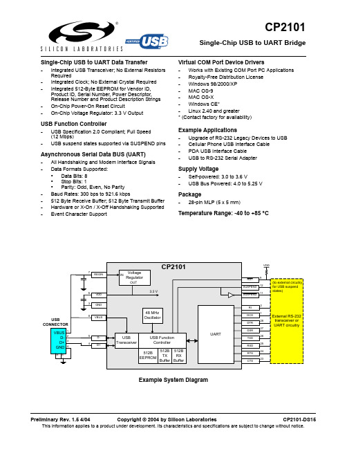
Single-Chip USB to UART BridgeCP2101Single-Chip USB to UART Data Transfer-Integrated USB Transceiver; No External Resistors Required-Integrated Clock; No External Crystal Required -Integrated 512-Byte EEPROM for Vendor ID, Product ID, Serial Number, Power Descriptor, Release Number and Product Description Strings -On-Chip Power-On Reset Circuit-On-Chip Voltage Regulator: 3.3 V OutputUSB Function Controller-USB Specification 2.0 Compliant; Full Speed (12 Mbps)-USB suspend states supported via SUSPEND pinsAsynchronous Serial Data BUS (UART)-All Handshaking and Modem Interface Signals -Data Formats Supported:•Data Bits: 8•Stop Bits: 1•Parity: Odd, Even, No Parity -Baud Rates: 300 bps to 921.6 kbps-512 Byte Receive Buffer; 512 Byte Transmit Buffer -Hardware or X-On / X-Off Handshaking Supported -Event Character SupportVirtual COM Port Device Drivers-Works with Existing COM Port PC Applications -Royalty-Free Distribution License -Windows 98/2000/XP -MAC OS-9-MAC OS-X -Windows CE*-Linux 2.40 and greater* (Contact factory for availability)Example Applications-Upgrade of RS-232 Legacy Devices to USB -Cellular Phone USB Interface Cable -PDA USB Interface Cable -USB to RS-232 Serial Adapter Supply Voltage-Self-powered: 3.0 to 3.6 V-USB Bus Powered: 4.0 to 5.25 V Package-28-pin MLP (5 x 5 mm)Temperature Range: -40 to +85 °CCP2101Table of Contents1.System Overview (4)2.Absolute Maximum Ratings (4)Table 2.1. Absolute Maximum Ratings (4)3.Global DC Electrical Characteristics (5)Table 3.1. Global DC Electrical Characteristics (5)Table 3.2. UART and Suspend I/O DC Electrical Characteristics (5)4.Pinout and Package Definitions (6)Table 4.1. Pin Definitions for the CP2101 (6)Figure 4.1. MLP-28 Pinout Diagram (Top View) (7)Figure 4.2. MLP-28 Package Drawing (8)Table 4.2. MLP-28 Package Dimensions (8)Figure 4.3. Typical MLP-28 Landing Diagram (9)Figure 4.4. Typical MLP-28 Solder Mask (10)B Function Controller and Transceiver (11)Figure 5.1. Typical Connection Diagram (11)6.Asynchronous Serial Data Bus (UART) Interface (12)Table 6.1. Data Formats and Baud Rates (12)7.Internal EEPROM (12)Table 7.1. Default USB Configuration Data (12)8.Virtual Com Port Device Drivers (13)9.Voltage Regulator (14)Table 9.1. Voltage Regulator Electrical Specifications (14)Figure 9.1. Configuration 1: USB Bus-Powered (14)Figure 9.2. Configuration 2: USB Self-Powered (15)Figure 9.3. Configuration 3: USB Self-Powered, Regulator Bypassed (15)1.System OverviewThe CP2101 is a highly-integrated USB-to-UART Bridge Controller providing a simple solution for updating RS-232 designs to USB using a minimum of components and PCB space. The CP2101 includes a USB 2.0 full-speed function controller, USB transceiver, oscillator, EEPROM and asynchronous serial data bus (UART) with full modem control signals in a compact 5 x 5 mm MLP-28 package. No other external USB components are required.The on-chip EEPROM may be used to customize the USB Vendor ID, Product ID, Product Description String, Power Descriptor, Device Release Number and Device Serial Number as desired for OEM applications. The EEPROM is programmed on-board via the USB allowing the programming step to be easily integrated into the product manufacturing and testing process.Royalty-free Virtual COM Port (VCP) device drivers provided by Silicon Laboratories allow a CP2101-based product to appear as a COM port to PC applications. The CP2101 UART interface implements all RS-232 signals, including control and handshaking signals, so existing system firmware does not need to be modified. In many existing RS-232 designs, all that is required to update the design from RS-232 to USB is to replace the RS-232 level-translator with the CP2101.An evaluation kit for the CP2101 (Part Number: CP2101EK) is available. It includes a CP2101-based USB-to-UART/RS-232 evaluation board, a complete set of VCP device drivers, USB and RS-232 cables, and full documentation. Contact a Silicon Labs’ sales representatives or go to to order the CP2101 Evaluation Kit.2.Absolute Maximum RatingsTable 2.1. Absolute Maximum RatingsParameter Conditions Min Typ Max Units Ambient temperature under bias–55—125°C Storage Temperature–65—150°C Voltage on any I/O Pin or RST with respect to–0.3— 5.8V GNDVoltage on V DD with respect to GND–0.3— 4.2V Maximum Total current through V DD and GND——500mA——100mA Maximum output current sunk by RST or anyI/O pinNote: stresses above those listed under “Absolute Maximum Ratings” may cause permanent damage to the device. This is a stress rating only and functional operation of the devices at those or any other condi-tions above those indicated in the operation listings of this specification is not implied. Exposure to maxi-mum rating conditions for extended periods may affect device reliability.CP21013.Global DC Electrical CharacteristicsTable 3.1. Global DC Electrical CharacteristicsV DD = 2.7 to 3.6 V, –40 to +85 °C unless otherwise specifiedParameter Conditions Min Typ Max Units Supply Voltage 3.0 3.3 3.6V Supply Current V DD = 3.3 V—25—mA Supply Current in Suspend V DD = 3.3 V—325—µA Specified Operating Temperature Range–40—+85°CTable 3.2. UART and Suspend I/O DC Electrical CharacteristicsV DD = 2.7 to 3.6 V, -40 to +85 °C unless otherwise specifiedParameters Conditions Min Typ Max UNITSOutput High Voltage I OH = -3mAI OH = -10µAI OH = -10mAVDD-0.7VDD-0.1VDD-0.8VOutput Low Voltage I OL = 8.5mAI OL = 10µAI OL = 25mA 1.00.60.1VInput High Voltage 2.0V Input Low Voltage0.8V Input Leakage Current2550µACP21014.Pinout and Package DefinitionsTable 4.1. Pin Definitions for the CP2101Name Pin #Type DescriptionV DD6Power InPowerOut3.0–3.6 V Power Supply Voltage Input.3.3 V Voltage Regulator Output. See Section 9.GND3GroundRST9 D I/O Device Reset. Open-drain output of internal POR or V DD monitor. An external source can initiate a system reset by driving this pin low for at least 15 µs.REGIN7Power In 5 V Regulator Input. This pin is the input to the on-chip voltage regu-lator.VBUS8 D In VBUS Sense Input. This pin should be connected to the VBUS signal of a USB network. A 5 V signal on this pin indicates a USB network connection.D+4 D I/O USB D+D–5 D I/O USB D–TXD26 D Out Asynchronous data output (UART Transmit) RXD25 D In Asynchronous data input (UART Receive) CTS23* D In Clear To Send control input (active low)RTS24* D Out Ready to Send control output (active low)DSR27* D in Data Set Ready control input (active low)DTR28* D Out Data Terminal Ready control output (active low) DCD1* D In Data Carrier Detect control input (active low)RI2* D In Ring Indicator control input (active low)SUSPEND12* D Out This pin is driven high when the CP2101 enters the USB suspend state.SUSPEND11* D Out This pin is driven low when the CP2101 enters the USB suspend state.NC10, 13–22These pins should be left unconnected or tied to V DD. *Note: Pins can be left unconnected when not used.CP2101Figure 4.1. MLP-28 Pinout Diagram (Top View)CP2101Figure 4.2. MLP-28 Package DrawingTable 0.1. MLP-28 Package DimensionsMM MIN TYP MAX A 0.800.90 1.00A100.020.05A200.65 1.00A3—0.25—b 0.180.230.30D — 5.00—D2 2.90 3.15 3.35E — 5.00—E2 2.90 3.15 3.35e —0.5—L 0.450.550.65N —28—ND —7—NE —7—R 0.09——AA —0.435—BB —0.435—CC —0.18—DD—0.18—CP2101Figure 4.3. Typical MLP-28 Landing DiagramCP2101Figure 4.4. Typical MLP-28 Solder Mask11Rev. 1.5B Function Controller and TransceiverThe Universal Serial Bus function controller in the CP2101 is a USB 2.0 compliant full-speed device with integrated transceiver and on-chip matching and pull-up resistors. The USB function controller manages all data transfers between the USB and the UART as well as command requests generated by the USB host controller and commands for controlling the function of the UART.The USB Suspend and Resume signals are supported for power management of both the CP2101 device as well as external circuitry. The CP2101 will enter Suspend mode when Suspend signaling is detected on the bus. On entering Suspend mode, the CP2101 asserts the SUSPEND and SUSPEND signals. SUSPEND and SUSPEND are also asserted after a CP2101 reset until device configuration during USB Enumeration is completeThe CP2101 exits the Suspend mode when any of the following occur: (1) Resume signaling is detected or generated, (2) a USB Reset signal is detected, or (3) a device reset occurs. On exit of Suspend mode, the SUSPEND and SUSPEND signals are de-asserted.Both SUSPEND and SUSPEND temporarily float high during a CP2101 reset. If this behavior is undesirable, a strong pulldown (10 kΩ) can be used to ensure SUSPEND remains low during reset. See Figure 5.1 for other recommended options.Figure 5.1. Typical Connection DiagramRev. 1.5126.Asynchronous Serial Data Bus (UART) InterfaceThe CP2101 UART interface consists of the TX (transmit) and RX (receive) data signals as well as the RTS, CTS, DSR, DTR, DCD and RI control signals. The UART supports RTS/CTS, DSR/DTR and X-On/X-Off handshaking.The UART is programmable to support a variety of data formats and baud rates. The data format and baud rate programmed into the UART is set during COM port configuration on the PC. The data formats and baud rates available are listed in Table 6.1.7.Internal EEPROMThe CP2101 includes an internal EEPROM that may be used to customize the USB Vendor ID, Product ID, Product Description String, Power Descriptor, Device Release Number and Device Serial Number as desired for OEM applications. Customization of the USB configuration data is optional. If the EEPROM is not programmed with OEM data, the default configuration data shown in Table 7.1 is used. However, a unique serial number is required for OEM applications in which it is possible for multiple CP2101-based devices to be connected to the same PC.The internal EEPROM is programmed via the USB. This allows the OEM's USB configuration data and serial number to be written to the CP2101 on-board during the manufacturing and testing process. A stand-alone utility for programming the internal EEPROM is available from Silicon Laboratories. A library of routines provided in the form of a Windows ® DLL is also available. This library can be used to integrate the EEPROM programming step into custom software used by the OEM to streamline testing and serial number management during manufacturing. The EEPROM has a typical endurance of 100,000 write cycles with a data retention of 100 years.Table 6.1. Data Formats and Baud RatesData Bits 8Stop Bits 1Parity Type None, Even, OddBaud Rates300, 600, 1200, 1800, 2400, 4800, 7200, 9600, 14400, 19200, 28800, 38400, 56000, 57600, 115200, 128000, 230400, 460800, 921600Table 7.1. Default USB Configuration DataName Value Vendor ID 10C4h Product IDEA60h Power Descriptor (Attributes)80hPower Descriptor (Max. Power)32h Release Number 0100hSerial Number0001 (63 characters maximum)Product Description String“CP2101 USB to UART Bridge Controller” (126 characters maximum)13Rev. 1.58.Virtual Com Port Device DriversThe CP2101 Virtual COM Port (VCP) device drivers allow a CP2101-based device to appear to the PC's application software as an additional COM port (in addition to any existing hardware COM ports). Application software running on the PC accesses the CP2101-based device as it would access a standard hardware COM port. However, actual data transfer between the PC and the CP2101 device is performed over the USB. Therefore, existing COM port applications may be used to transfer data via the USB to the CP2101-based device without modifying the application. Contact Silicon Laboratories for the latest list of supported operating systems.Note:The Silicon Laboratories VCP device drivers are required for device operation and are only distributed as part of the CP2101 Evaluation Kit (Part Number: CP2101EK). Contact any of Silicon Lab’s sales representatives or go to to order the CP2101 Evaluation Kit. The CP2101 drivers and programming utilities are subject to change without notice. Subscription to the website "Auto Email Alert" system for automatic notification of updates and the use of the "Product Update Registration" service is recommended.Rev. 1.5149.Voltage RegulatorThe CP2101 includes an on-chip 5-to-3 V voltage regulator. This allows the CP2101 to be configured as either a USB bus-powered device or a USB self-powered device. These configurations are shown in Figure 9.1 and Figure 9.2. When enabled, the 3 V voltage regulator output appears on the V DD pin and can be used to power external 3V devices. See Table 9.1 for the voltage regulator electrical characteristics.Alternatively, if 3 V power is supplied to the V DD pin, the CP2101 can function as a USB self-powered device with the voltage regulator disabled. For this configuration, it is recommended that the REGIN input be tied to the 3 V net to disable the voltage regulator. This configuration is shown in Figure 9.3.The USB max power and power attributes descriptor must match the device power usage and configuration. See application note “AN144: CP2101 Customization Guide” for information on how to customize USB descriptors for the CP2101.Note:It is recommended that additional decoupling capacitance (e.g., 0.1 µF in parallel with 1.0 µF) be provided on the REGIN input.Figure 9.1. Configuration 1: USB Bus-PoweredTable 9.1. Voltage Regulator Electrical Specifications–40 to +85 °C unless otherwise specifiedParameterConditionsMin Typ Max Units Input Voltage Range 4.0— 5.25V Output VoltageOutput Current = 1 to 100 mA*3.0 3.3 3.6V VBUS Detection Input Threshold 1.0 1.84.0V Bias Current—90TBDµA* The maximum regulator supply current is 100 mA.15Rev. 1.5Figure 9.2. Configuration 2: USB Self-PoweredFigure 9.3. Configuration 3: USB Self-Powered, Regulator BypassedRev. 1.516Document Change ListRevision 1.4 to Revision 1.5Updated Example System Diagram on page 1.Updated Table 3.1, “Global DC Electrical Characteristics,” on page 5.Added Table 3.2, “UART and Suspend I/O DC Electrical Characteristics,” on page 5 Added Table note to Table 4.1, “Pin Definitions for the CP2101,” on page 6 Added Figure 5.1. , "Typical Connection Diagram" on page 11Removed asterisk from the “Linux 2.40 and greater” bullet on page 117Rev. 1.5NotesRev. 1.518Contact InformationSilicon Laboratories Inc.4635 Boston Lane Austin, TX 78735Tel: 1+(512) 416-8500 Fax: 1+(512) 416-9669 Toll Free: 1+(877) 444-3032Email:********************** Internet: Silicon Laboratories and Silicon Labs are trademarks of Silicon Laboratories Inc.Other products or brandnames mentioned herein are trademarks or registered trademarks of their respective holdersThe information in this document is believed to be accurate in all respects at the time of publication but is subject to change without notice. Silicon Laboratories assumes no responsibility for errors and omissions, and disclaims responsibility for any consequences resulting from the use of information included herein. Additionally, Silicon Laboratories assumes no responsibility for the function-ing of undescribed features or parameters. Silicon Laboratories reserves the right to make changes without further notice. Silicon Laboratories makes no warranty, representation or guarantee regarding the suitability of its products for any particular purpose, nor does Silicon Laboratories assume any liability arising out of the application or use of any product or circuit, and specifically disclaims any and all liability, including without limitation consequential or incidental damages. Silicon Laboratories products are not designed, intended, or authorized for use in applications intended to support or sustain life, or for any other application in which the failure of the Silicon Laboratories product could create a situation where personal injury or death may occur. Should Buyer purchase or use Silicon Laboratories products for any such unintended or unauthorized application, Buyer shall indemnify and hold Silicon Laboratories harmless against all claims and damages.。
CP2102(USB转UART)

Section
Page
1. System Overview . . . . . . . . . . . . . . . . . . . . . . . . . . . . . . . . . . . . . . . . . . . . . . . . . . . . . . . . .4 2. Absolute Maximum Ratings . . . . . . . . . . . . . . . . . . . . . . . . . . . . . . . . . . . . . . . . . . . . . . . .4 3. Global DC Electrical Characteristics . . . . . . . . . . . . . . . . . . . . . . . . . . . . . . . . . . . . . . . . .5 4. Pinout and Package Definitions . . . . . . . . . . . . . . . . . . . . . . . . . . . . . . . . . . . . . . . . . . . . .6 5. USB Function Controller and Transceiver . . . . . . . . . . . . . . . . . . . . . . . . . . . . . . . . . . . . 11 6. Asynchronous Serial Data Bus (UART) Interface . . . . . . . . . . . . . . . . . . . . . . . . . . . . . . 12 7. Internal EEPROM . . . . . . . . . . . . . . . . . . . . . . . . . . . . . . . . . . . . . . . . . . . . . . . . . . . . . . . . 12 8. CP2101 Device Drivers . . . . . . . . . . . . . . . . . . . . . . . . . . . . . . . . . . . . . . . . . . . . . . . . . . .13
刷机线USB转串口TTL线使用方法简介

刷机线USB转串口TTL线使用方法简介USB转串口TTL小板安装测试:1.首先安装USB转串口的驱动程序(USB转串口驱动下载地址)2.下载串口调试助手用于测试小板好坏以及性能(串口调试助手下载地址)3.用一根杜邦线或短接冒短接小板上的TXD和RXD 端口4.把小板插到计算机的USB端口上,首次计算机会检测到新硬件并自动安装,小板电源指示灯亮5.进入计算机的“设备管理器”查看系统分配的端口号即COM?,同一计算机不同USB口分配的端口号是不同的(进入设备管理器方法查看)6.打开串口调试助手,设置好端口号(即COM?号)和波特率后点击“连接”,如果“连接”前面的灯变为红色说明打开串口成功7.在发送窗口设置好要发送的内容,点击“发送“,如果在接收窗口接收到的内容与发送的内容相同说明小板完好(测试示意图查看)USB转TTL小板与USB转RS232小板区别:B转TTL小板插上USB口后,电源指示灯为红色;而USB转RS232小板插上USB口后,电源指示灯为黄色B转TTL小板板上有一些元件没有安装;而USB转RS232小板上的元件是完全安装了的B转TTL小板是TTL电平,可直接与5V电平相接;而USB转RS232小板是标准RS232电平,可直接与计算机的串口相接,二者不能混用接收机接线方法:1.关掉接收机电源,打开接收机机壳,先查看升级端口在板子上没有没RXD、TXD、GND、VCC等字样标识,如果有进入第4步,否则继续2.关掉接收机电源,用万用表电阻档先找出地线GND。
(10欧姆以下)3.打开接收机电源,再用万用表电压档找出 RXD和TXD两根信号线。
(RXD电压一般小于2v,txd电压一般小于4v,有部分的接收机是没有电压输出的。
)4.将小板RXD与接收机的TXD连接,小板TXD与接收机RXD连接,小板GND与接收机GND连接5.电源VDD一般不用接,但有部分的接收机一定要接才能升级。
(电压一定小于5.5v)6.如果不能联机将RXD TXD 互调一下。
单路USB转多路串口方案分享

单路USB转多路串口方案分享串口,对于从事电子行业的朋友应该再也熟悉不过了,它是一种非常通用的设备通信的协议,大多数台式机箱都有RS232-DB9的接口,而且还有多个USB接口。
笔记本电脑通常只有3个USB口,而没有DB9端口,如果想使用串口功能,只能使用USB-TTL模块。
如果需要多个串口时,就要占用多个USB口,再加上鼠标、调试器等,PC提供的USB口就不够用了。
本文分享几种使用单USB口转多路串口的方案,串口之间相互独立,互不干扰。
1. CH9342单芯片实现双串口如果你最多只需要两路串口,那么CH9342是个不错的选择,它是一款单路USB转双串口芯片,提供两组全双工的9线异步串口UART0/1,用于为计算机扩展异步串口,或者将普通的串口设备升级到USB总线。
应用电路:评估板:2. CH9344单芯片实现4路串口如果两路串口不够用,不用担心,我们还有4路串口芯片,CH9344是一款单路USB转4串口控制芯片,提供4组全双工的异步串口UART0/1/2/3,用于为计算机扩展异步串口,或者将普通的串口设备升级到USB总线。
外部只需要一个30M的晶体和少量的电容即可使用,支持波特率1200-7.8125Mbps,LQFP-48封装。
应用电路:评估板:3. CH934X+CH438实现多串口如果需要更多的串口,可以试试CH934X配合CH438的方式。
CH943X是USB转多串口控制芯片,主要负责处理USB接口所有数据传输,并通过并行接口操作CH438,实现多个串口数据的接收和发送。
安装好驱动后,插入USB转串口模块,在电脑上会出现多个串口,这些串口操作方式上和电脑自带的串口一模一样,各个串口相互独立,互不干扰。
USB转多串口应用图如下:N可以为2、4、8、16,波特率支持1200-921600bps,各个串口操作与电脑自带硬件串口一模一样,相互独立,互不干扰。
在官网上并没有找到相关的应用资料,可能需要联系厂家获取资料。
USB转TTL模块使用说明.doc
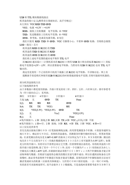
小常识(非常重要):TXD:发送端,一般表示为自己的发送端,正常通信必须接另一个设备的RXD。
RXD:接收端,一般表示为自己的接收端,正常通信必须接另一个设备的TXD。
正常通信时候本身的TXD永远接设备的RXD!自收自发:正常通信时RXD接其他设备的TXD,因此如果要接收自己发送的数据顾名思义,也就是自己接收自己发送的数据,即自身的TXD直接连接到RXD,用来测试本身的发送和接收是否正常,是最快最简单的测试方法,当出现问题时首先做该测试确定是否产品故障。
也称回环测试。
电平逻辑:TTL电平:通常数据表示采用二进制,规定+5V等价于逻辑"1",0V等价于逻辑"0",称作TTL信号系统,是正逻辑RS232电平:采用-12V到-3V,等价于逻辑"0",+3V到+12V的逻辑电平,等价于逻辑"1",是负逻辑的产品说明:1、主芯片为CP2102,安装驱动后生成虚拟串口2、USB取电,引出接口包括3.3V(<40mA),5V,GND,TX,RX,信号脚电平为3.3V,正逻辑3、板载状态指示灯、收发指示灯,正确安装驱动后状态指示灯会常亮,收发指示灯在通信的时候会闪烁,波特率越高亮度越低4、支持从300bps~1Mbps间的波特率5、通信格式支持:1)5,6,7,8位数据位;2)支持1,1.5,2停止位;3)odd,even,mark,space,none校验6、支持操作系统:windows vista/xp/server 2003/200,MacOS-X/OS-9,Linux7、USB头为公头,可直接连接电脑USB口8、贴片元件为SMT工艺生产,质量稳定9、不含USB头体积为:33*15(mm)购买该产品包括以下配件:1、焊接测试好的模块一个2、20cm长4P杜邦线一条注:该USB转串口可以用STC-ISPV3.94以上版本下载STC旧版本单片机即STC89C(LE)和STC12C(LE)系列(新版本芯片不一定能下载,有网友将软件上最高和最低波特率设置为一样时可以下载,我们不对此做保证,请自行斟酌)(STC-ISP下载地址<复制到浏览器地址栏>:/datasheet/stc/STC-ISP-V4.83/STC-ISP -V4.83-NOT-SETUP-CHINESE.EXE,下载后解压缩即可)请看清楚,这不是驱动!下载STC单片机步骤:TXD接到单片机的RXD,RXD接单片机的TXD,GND 接GND,5V接VCC,在软件上点下载,然后再把上面说的四个脚插到单片机上。
USB转TTL模块数据线接法
USB转TTL模块数据线接法机顶盒的接口定义(顺带讲点基础知识,高手可略过)从左到右VCC RXD TXD GNDVCC:电源+3.2V -> +3.3VRXD:接收上位机数据电平范围:0->VCCTXD:发送数据给上位机电平范围:0->VCCGND:参考地,也就是电源负极,0电位我们只使用RXD TXD和GND,VCC引脚要小心,不要和GND短路,否则将会烧毁LOD(稳压)芯片机顶盒的RXD接RS232的TXD机顶盒的TXD接RS232的RXD机顶盒的GND接RS232的GND我们将上述电平范围的通讯电平称作TTL电平而RS232通讯端口(计算机原本的RS232口和用USB接口转出的标准RS232口)的标准电平范围是+15V->-15V。
所以需要做电平转换。
当然有些USB转RS232也有TTL电平输出的。
我这里是使用一个已有的单片机的下载器上的RS232电平转换,不详细讨论,网上有提醒新手的是购买和使用USB转RS232的时候要搞清楚电平范围,否则可能损坏机器的。
部分机顶盒接线方法以下接线图供参考由于多数接口都是使用排插,升级口常见的有三针、四针、五针、六针和九针,排序参看考为(针口面向自己),见列表:脚位3针接口4针接口5针接口6针接口左起1(6) 无GND TX None2(5) RX RX RX GND3(4) TX TX VCC1RX4(3)VCC(3.3V)VCC(3.3V)GND TX5(2) 无Vcc2 VCC(3.3V)6(1) 无None4线升级接口:1脚--接地,2脚--RX ,3脚--TX ,4脚--VCC ,(卓异) 5脚--不接6线升级接口:1脚—空,2脚--接地,3脚--RX,4脚--TX,5脚--VCC,6脚—空以上仅仅是供参考首先先找出接地引脚GND(红笔接射频线金属,再用黑笔测量各个针脚,0阻值导通即为地GND),确定好GND后,再将机顶盒通电,再测量各针脚空载时的电压,即黑表笔接地,红表笔测出的电压是3.36V~3.30V的基本上可以判定为TXD、RXD的针脚,测出的电压在5V左右的为VCC(负载在数据线MX232芯片上有可能降为3.3V这样),如果是五针的升级口,有的可以不需理会而让它空置,但需要特别注意的是,有的机顶盒的5针的升级口很是特殊,除了其中一个VCC1外,还有一个引脚为Vcc2(有的标识为BL),空载电压大概是1.65V这样,在刷新时就必须将VCC1和Vcc2两个针脚短接才能正常读取和烧写数据,否则读写速度将会极其的慢以至读写都不成功,所以在遇到读取备份文件很慢时,就必须考虑将两个针脚进行短接才能读写数据,而使用此两个针脚短接的方法也可激活变成砖头的机器(后面再具体阐述)。
- 1、下载文档前请自行甄别文档内容的完整性,平台不提供额外的编辑、内容补充、找答案等附加服务。
- 2、"仅部分预览"的文档,不可在线预览部分如存在完整性等问题,可反馈申请退款(可完整预览的文档不适用该条件!)。
- 3、如文档侵犯您的权益,请联系客服反馈,我们会尽快为您处理(人工客服工作时间:9:00-18:30)。
Rev. 1.1 11/13Copyright © 2013 by Silicon LaboratoriesCP2105CP2105S INGLE -C HIP USB TO D UAL UART B RIDGESingle-Chip USB to Dual UART Data Transfer● Integrated USB transceiver; no external resistorsrequired● Integrated clock; no external crystal required● Integrated 296-Byte One-Time Programmable ROM for storing customizable product information ● On-chip power-on reset circuit● On-chip voltage regulator: 3.45V outputUSB Peripheral Function Controller● USB Specification 2.0 compliant; full-speed (12Mbps)● USB Suspend states supported via SUSPEND pinsTwo UART Interfaces (“Enhanced” and “Standard”)● Flow control options:-Hardware (CTS / RTS)-Software (X-On / X-Off)-No flow control● Configurable I/O (1.8V to V DD ) using V IO pin● Configurable I/O (V DD to 5V) using external pull-up● All modem interface signals available (when GPIO is notused)Enhanced UART Interface Features● Data formats supported:-Data bits: 5, 6, 7, and 8-Stop bits: 1, 1.5, and 2-Parity: odd, even, mark, space, no parity ● Baud rates: 300bps to 2.0Mbps● 320 Byte receive and transmit buffers ● Two GPIO signals for status and control ● RS-485 mode with bus transceiver controlStandard UART Interface Features● Data format: 8 data bits, 1 Stop bit ● Parity: Even, Odd, No parity ● Baud rates: 2400bps to 921600bps● 288 Byte receive and transmit buffers ● Three GPIO signals for status and controlVirtual COM Port Device Drivers● Works with Existing COM Port PC Applications ● Royalty-Free Distribution License ● Windows 7/Vista/XP/Server 2003/2000● Mac OS-X ● LinuxUSBXpress™ Direct Driver Support● Royalty-Free Distribution License ● Windows 7/Vista/XP/Server 2003/2000● Windows CE 6.0, 5.0, and 4.2Supply Voltage● Self-powered: 3.0 to 3.6V● USB bus powered: 4.0 to 5.25V ● I/O voltage: 1.8V to V DDPackage● RoHS-compliant 24-pin QFN (4 x 4mm)Ordering Part Number● CP2105-F01-GMTemperature Range: –40 to +85°CCP21052Rev. 1.1CP2105Rev. 1.13T ABLE OF C ONTENTSSectionPage1. System Overview . . . . . . . . . . . . . . . . . . . . . . . . . . . . . . . . . . . . . . . . . . . . . . . . . . . . . . . . .42. Electrical Characteristics . . . . . . . . . . . . . . . . . . . . . . . . . . . . . . . . . . . . . . . . . . . . . . . . . .53. Pinout and Package Definitions . . . . . . . . . . . . . . . . . . . . . . . . . . . . . . . . . . . . . . . . . . . . .84. QFN-24 Package Specifications . . . . . . . . . . . . . . . . . . . . . . . . . . . . . . . . . . . . . . . . . . . .115. USB Function Controller and Transceiver . . . . . . . . . . . . . . . . . . . . . . . . . . . . . . . . . . . .136. Asynchronous Serial Data Bus (UART) Interfaces . . . . . . . . . . . . . . . . . . . . . . . . . . . . .136.1. ECI Baud Rate Generation . . . . . . . . . . . . . . . . . . . . . . . . . . . . . . . . . . . . . . . . . . . .147. GPIO Mode and Modem Mode . . . . . . . . . . . . . . . . . . . . . . . . . . . . . . . . . . . . . . . . . . . . . .148. GPIO Pins . . . . . . . . . . . . . . . . . . . . . . . . . . . . . . . . . . . . . . . . . . . . . . . . . . . . . . . . . . . . . .158.1. GPIO.0-1—Transmit and Receive Toggle . . . . . . . . . . . . . . . . . . . . . . . . . . . . . . . .158.2. GPIO.1_ECI—RS-485 Transceiver Bus Control . . . . . . . . . . . . . . . . . . . . . . . . . . . .168.3. Hardware Flow Control (RTS and CTS) . . . . . . . . . . . . . . . . . . . . . . . . . . . . . . . . . .179. One-Time Programmable ROM . . . . . . . . . . . . . . . . . . . . . . . . . . . . . . . . . . . . . . . . . . . . .1810. Voltage Regulator . . . . . . . . . . . . . . . . . . . . . . . . . . . . . . . . . . . . . . . . . . . . . . . . . . . . . . .1911. CP2105 Device Drivers . . . . . . . . . . . . . . . . . . . . . . . . . . . . . . . . . . . . . . . . . . . . . . . . . .2111.1. Virtual COM Port Drivers . . . . . . . . . . . . . . . . . . . . . . . . . . . . . . . . . . . . . . . . . . . . .2111.2. USBXpress Drivers . . . . . . . . . . . . . . . . . . . . . . . . . . . . . . . . . . . . . . . . . . . . . . . . .2111.3. Driver Customization . . . . . . . . . . . . . . . . . . . . . . . . . . . . . . . . . . . . . . . . . . . . . . . .2111.4. Driver Certification . . . . . . . . . . . . . . . . . . . . . . . . . . . . . . . . . . . . . . . . . . . . . . . . . .2112. Relevant Application Notes . . . . . . . . . . . . . . . . . . . . . . . . . . . . . . . . . . . . . . . . . . . . . . .22Document Change List . . . . . . . . . . . . . . . . . . . . . . . . . . . . . . . . . . . . . . . . . . . . . . . . . . . . .23Contact Information . . . . . . . . . . . . . . . . . . . . . . . . . . . . . . . . . . . . . . . . . . . . . . . . . . . . . . . .24CP21054Rev. 1.11. System OverviewThe CP2105 is a highly integrated USB-to-Dual-UART Bridge Controller providing a simple solution for updating RS-232 designs to USB using a minimum of components and PCB space. The CP2105 includes a USB 2.0 full-speed function controller, USB transceiver, oscillator, one-time programmable ROM, and two asynchronous serial data buses (UART) with full modem control signals in a compact 4x4mm QFN-24 package (sometimes called “MLF” or “MLP”).The on-chip one-time programmable ROM may be used to customize the USB Vendor ID, Product ID, Product Description String, Power Descriptor, Device Release Number, Interface Strings, Device Serial Number, and Modem/GPIO configuration as desired for OEM applications.Royalty-free Virtual COM Port (VCP) device drivers provided by Silicon Labs allow a CP2105-based product to appear as two COM ports in PC applications. The CP2105 UART interfaces implement all RS-232 signals including control and handshaking, so existing system firmware does not need to be modified. The device also features a total of five GPIO signals that can be user-defined for status and control information. Support forI/O interface voltages down to 1.8V is provided via a V IO pin. Direct access driver support is also available through the Silicon Labs USBXpress driver set. See for the latest application notes and product support information for the CP2105.An evaluation kit for the CP2105 (Part Number: CP2105EK) is available. It includes a CP2105-based USB-to-UART/RS-232 evaluation board, a complete set of VCP device drivers, USB and RS-232 cables, and full documentation. Contact a Silicon Labs sales representatives or go to to order the CP2105 Evaluation Kit.CP2105Rev. 1.152. Electrical CharacteristicsTable 1. Absolute Maximum RatingsParameterTest ConditionMin Typ Max Unit Ambient Temperature Under Bias –55—125°C Storage Temperature–65—150°C Voltage on RST, GPIO or UART Pins with respect to GNDV IO > 2.2V V IO < 2.2V –0.3–0.3—— 5.8V IO + 3.6VVoltage on VBUS with respect to GNDV DD > 3.0V V DD not powered –0.3–0.3—— 5.8V DD + 3.6VVoltage on V DD or V IO with respect to GND –0.3— 4.2V Maximum Total Current through V DD , V IO , and GND ——500mA Maximum Output Current Sunk by RST or any I/O pin——100mANote:Stresses above those listed may cause permanent damage to the device. This is a stress rating only, and functionaloperation of the devices at or exceeding the conditions in the operation listings of this specification is not implied. Exposure to maximum rating conditions for extended periods may affect device reliability.Table 2. Global DC Electrical CharacteristicsV DD =3.0 to 3.6V, –40 to +85 °C unless otherwise specified.ParameterTest Condition Min Typ Max Unit Digital Supply Voltage (V DD ) 3.0— 3.6V Digital Port I/O Supply Voltage (V IO ) 1.8—V DD V Voltage on V PP with respect to GND during a ROM programming operationV IO > 3.3V5.75—V IO + 3.6V Capacitor on V PP for ROM programming —4.7—µF Supply Current 1Normal Operation; V REG Enabled —1718.5mA Supply Current 1Suspended;V REG Enabled—100220µA Supply Current - USB Pull-up 2—200228µA Specified Operating Temperature Range–40—+85°CNotes:1.If the device is connected to the USB bus, the USB Pull-up Current should be added to the supply current for totalsupply current.2. The USB Pull-up supply current values are calculated values based on USB specifications.CP21056Rev. 1.1Table 3. UART and Suspend I/O DC Electrical CharacteristicsV DD=3.0 to 3.6V, V IO=1.8 V to V DD, –40 to +85°C unless otherwise specified.Parameters Test Condition Min Typ Max UnitOutput High Voltage (V OH)I OH=–10µAI OH=–3mAI OH=–10mA V IO–0.1V IO–0.2———V IO–0.4———VOutput Low Voltage (V OL)I OL=10µAI OL=8.5mAI OL=25mA —————0.60.10.4—VInput High Voltage (V IH)0.7 x V IO——V Input Low Voltage (V IL)——0.6VInput Leakage Current Weak Pull-Up OffWeak Pull-Up On, V IO=0V ———25150µAMaximum Input Voltage Open drain, logic high (1)—— 5.8V Table 4. Reset Electrical Characteristics–40 to +85 °C unless otherwise specified.Parameter Test Condition Min Typ Max Unit RST Input High Voltage0.75 x V IO——V RST Input Low Voltage——0.6V Minimum RST Low Time toGenerate a System Reset15——µs V DD Ramp Time for Power On——1msTable 5. Voltage Regulator Electrical Specifications–40 to +85°C unless otherwise specified.Parameter Test Condition Min Typ Max Units Input Voltage Range 3.0— 5.25V Output Voltage Output Current=1 to 100mA* 3.3 3.45 3.6V VBUS Detection Input Threshold 2.5——V Bias Current——120µA *Note:The maximum regulator supply current is 100mA. This includes the supply current of the CP2105.CP2105Rev. 1.17Table 6. GPIO Output Specifications–40 to +85 °C unless otherwise specified.ParameterTest ConditionMin Typ Max Unit RS-485 Active Time After Stop Bit —1—bit time*TX Toggle Rate —7.5—Hz RX Toggle Rate—7.5—Hz*Note: Bit-time is calculated as 1 / baud rate.CP21058Rev. 1.13. Pinout and Package DefinitionsTable 7. CP2105 Pin Definitions Name Pin #Type DescriptionV DD6Power InPower Out Power Supply Voltage Input.Voltage Regulator Output. See Section 10.V IO5Power In I/O Supply Voltage Input.GND2Ground. Must be tied to ground.RST9 D I/O Device Reset. Open-drain output of internal POR or V DD monitor. An externalsource can initiate a system reset by driving this pin low for the time specifiedin Table4.REGIN7Power In5V Regulator Input. This pin is the input to the on-chip voltage regulator. VBUS8 D In VBUS Sense Input. This pin should be connected to the VBUS signal of aUSB network.D+3 D I/O USB D+D–4 D I/O USB D–SUSPEND RI_SCI 1* D OutD InIn GPIO mode, this pin indicates whether the device is in the USB Suspend ornot. The polarity can be configured via the configuration PROM, and defaultsto active-low.In modem control mode, this pin is the Ring Indicator control input (active low)for the Standard Comm Interface.GPIO.0_SCI DCD_SCI 24* D I/OD InIn GPIO mode, this pin is a user-configurable input or output for the StandardComm Interface.In modem control mode, this pin is the Data Carrier Detect control input(active low) for the Standard Comm Interface.GPIO.1_SCI DTR_SCI 23* D I/OD OutIn GPIO mode, this pin is a user-configurable input or output for the StandardComm Interface.In modem control mode, this pin is the Data Terminal Ready control output(active low) for the Standard Comm Interface.GPIO.2_SCI DSR_SCI 22* D I/OD inIn GPIO mode, this pin is a user-configurable input or output for the StandardComm Interface.In modem control mode, this pin is the Data Set Ready control input (activelow) for the Standard Comm Interface.TXD_SCI21 D Out Asynchronous data output (UART Transmit) for the Standard Comm Inter-face.RXD_SCI20 D In Asynchronous data input (UART Receive) for the Standard Comm Interface.RTS_SCI19* D Out Ready to Send control output (active low) for the Standard Comm Interface. *Note:Pins can be left unconnected when not used.CP2105Rev. 1.19CTS_SCI 18* D In Clear To Send control input (active low) for the Standard Comm Interface.SUSPENDRI_ECI 17*D OutD In In GPIO mode, this pin indicates whether the device is in the USB Suspend or not. The polarity can be configured via the configuration PROM, and defaults to active-low.In modem control mode, this pin is the Ring Indicator control input (active low) for the Standard Comm Interface.NC DCD_ECIV PP16*—D InSpecialIn GPIO mode, this pin is not used.In modem control mode, this pin is the Data Carrier Detect control input (active low) for the Enhanced Comm Interface.Additionally, in either mode programming of the configuration ROM via the USB interface can be accomplished if a 4.7 F capacitor is connected between this pin and GND.GPIO.0_ECI DTR_ECI 15* D I/OD Out In GPIO mode, this pin is a user-configurable input or output for the Enhanced Comm Interface.In modem control mode, this pin is the Data Terminal Ready control output (active low) for the Enhanced Comm Interface.GPIO.1_ECIDSR_ECI 14*D I/OD in In GPIO mode, this pin is a user-configurable input or output for the Enhanced Comm Interface.In modem control mode, this pin is the Data Set Ready control input (active low) for the Enhanced Comm Interface.TXD_ECI 13 D Out Asynchronous data output (UART Transmit) for the Enhanced Comm Inter-face.RXD_ECI 12 D In Asynchronous data input (UART Receive) for the Enhanced Comm Interface.RTS_ECI 11* D Out Ready to Send control output (active low) for the Enhanced Comm Interface.CTS_ECI10*D InClear To Send control input (active low) for the Enhanced Comm Interface.Table 7. CP2105 Pin Definitions (Continued)Name Pin #Type Description*Note: Pins can be left unconnected when not used.CP210510Rev. 1.1Figure2.QFN-24 Pinout Diagram (Top View)4. QFN-24 Package SpecificationsFigure3.QFN-24 Package DrawingTable 8. QFN-24 Package DimensionsDimension Min Typ Max Dimension Min Typ Max A0.700.750.80L0.300.400.50A10.000.020.05L10.00—0.15b0.180.250.30aaa——0.15D 4.00 BSC.bbb——0.10D2 2.55 2.70 2.80ddd——0.05e0.50 BSC.eee——0.08E 4.00 BSC.Z—0.24—E2 2.55 2.70 2.80Y—0.18—Notes:1.All dimensions shown are in millimeters (mm) unless otherwise noted.2. Dimensioning and Tolerancing per ANSI Y14.5M-1994.3. This drawing conforms to JEDEC Solid State Outline MO-220, variation WGGD except forcustom features D2, E2, Z, Y, and L, which are toleranced per supplier designation.4. Recommended card reflow profile is per the JEDEC/IPC J-STD-020 specification for Small BodyComponents.Figure4.QFN-24 Recommended PCB Land PatternTable 9. QFN-24 PCB Land Pattern DimensionsDimension Min Max Dimension Min Max C1 3.90 4.00X2 2.70 2.80C2 3.90 4.00Y10.650.75E0.50 BSC Y2 2.70 2.80X10.200.30Notes:General1.All dimensions shown are in millimeters (mm) unless otherwise noted.2. This Land Pattern Design is based on the IPC-7351 guidelines.Solder Mask Design3. All metal pads are to be non-solder mask defined (NSMD). Clearance between the soldermask and the metal pad is to be 60 m minimum, all the way around the pad.Stencil Design4. A stainless steel, laser-cut and electro-polished stencil with trapezoidal walls should be usedto assure good solder paste release.5. The stencil thickness should be 0.125mm (5 mils).6. The ratio of stencil aperture to land pad size should be 1:1 for all perimeter pads.7. A 2x2 array of 1.10 x 1.10mm openings on a 1.30mm pitch should be used for the centerpad.Card Assembly8. A No-Clean, Type-3 solder paste is recommended.9. The recommended card reflow profile is per the JEDEC/IPC J-STD-020 specification for SmallBody Components.5. USB Function Controller and TransceiverThe Universal Serial Bus (USB) function controller in the CP2105 is a USB 2.0 compliant full-speed device with integrated transceiver and on-chip matching and pullup resistors. The USB function controller manages all data transfers between the USB and the UARTs as well as command requests generated by the USB host controller and commands for controlling the function of the UARTs and GPIO pins.The USB Suspend and Resume states are supported for power management of both the CP2105 device as well as external circuitry. The CP2105 will enter Suspend mode when Suspend signaling is detected on the bus. On entering Suspend mode, the SUSPEND signals will be asserted if the corresponding interface is configured for GPIO mode. SUSPEND is also asserted after a CP2105 reset until device configuration during USB Enumeration is complete. SUSPEND is active-low by default, but can be configured using the PROM to be active high.The CP2105 exits the Suspend mode when any of the following occur: Resume signaling is detected or generated, a USB Reset signal is detected, or a device reset occurs. On exit of Suspend mode the SUSPEND signal is de-asserted. SUSPEND is weakly pulled to VIO in a high impedance state during a CP2105 reset. If this behavior is undesirable, a strong pulldown (10k ) can be used to ensure SUSPEND remains low during reset.The logic level and output mode (push-pull or open-drain) of various pins during USB Suspend is configurable in the PROM. See Section 9 for more information.6. Asynchronous Serial Data Bus (UART) InterfacesThe CP2105 contains two UART interfaces, known as the Enhanced Communications Interface (ECI) and Standard Communications Interface (SCI)Each UART interface consists of the TXD (transmit) and RXD (receive) data signals as well as RTS and CTS flow control signals. Optionally, the modem control signals DSR, DTR, DCD, and RI can be enabled for each interface. If modem control signals are not required for the application, these pins can be configured to operate with alternate functions, such as GPIO and SUSPEND signals. The UARTs support RTS/CTS, DSR/DTR, and X-On/X-Off handshaking. The UARTs are programmable to support a variety of data formats and baud rates. The ECI supports several additional UART configuration options beyond those supported by the SCI. If the Virtual COM Port drivers are used, the data format and baud rate are set during COM port configuration on the PC. If the USBXpress drivers are used, the CP2105 is configured through the USBXpress API. The data formats and baud rates available to each interface are listed in Table10.Table 10. Data Formats and Baud RatesInterface Enhanced Communication Interface (ECI)Standard Communication Interface (SCI) Data Bits15, 6, 7, and 88Stop Bits1, 1.52, and 21Parity Type None, Even, Odd, Mark, Space None, Even, OddBaud Rate300bps to 2.0Mbps32400, 4800, 7200, 9600, 14400, 19200, 28800, 38400, 56000, 57600, 115200, 128000, 230400, 460800, 921600Notes:1.Data sizes of 5 and 6 bits are not supported at baud rates above 921600bps.2. 1.5 stop bits only available when using 5 data bits.3. See “6.1. ECI Baud Rate Generation” for more details on possible baud rates for the ECI interface.6.1. ECI Baud Rate GenerationThe baud rate generator for the enhanced interface is very flexible, allowing the user to request any baud rate in the range from 300bps to 2.0Mbps. If the baud rate cannot be directly generated from the 48MHz oscillator, the device will choose the closest possible option. The actual baud rate is dictated by Equation 1 and Equation 2.Equation 1.Clock Divider CalculationEquation 2.Baud Rate CalculationMost baud rates can be generated with an error of less than 1.0%. A general rule of thumb for the majority of UART applications is to limit the baud rate error on both the transmitter and the receiver to no more than ±2%. The clock divider value obtained in Equation 1 is rounded to the nearest integer, which may produce an error source. Another error source will be the 48MHz oscillator, which is accurate to ±0.25%. Knowing the actual and requested baud rates, the total baud rate error can be found using Equation 3.Equation 3.Baud Rate Error CalculationThe UART also supports the transmission of a line break. The length of time for a line break is programmable from1 to 125ms, or it can be set to transmit indefinitely until a stop command is sent from the application.7. GPIO Mode and Modem ModeEach interface on the CP2105 can be configured in either GPIO Mode or Modem Mode. This allows the SCI and ECI to have either modem control signals or GPIO signals available at various pins. Table 11 shows the functions that are available in each mode.By default, both interfaces are configured for GPIO Mode.Only one mode can be selected for each interface. Also, the mode of the CP2105 can only be configured once and cannot be reset to the default configuration after being programmed. Refer to “AN223: Runtime GPIO Control for CP210x” for more information on how to configure the port pins of the CP2105.Table 11. CP2105 Modem Mode and GPIO ModeInterfacePin #Modem Mode GPIO Mode Standard CommunicationsInterface24DCD_SCI GPIO_0_SCI 23DTR_SCI GPIO_1_SCI 22DSR_SCI GPIO_2_SCI 1RI_SCI SUSPEND_SCI Enhanced CommunicationsInterface15DTR_ECI GPIO_0_ECI 14DSR_ECI GPIO_1_ECI 17RI_ECISUSPEND_ECIClock Divider 48MHz2Prescale Requested Baud Rate⨯⨯----------------------------------------------------------------------------------------------------=Prescale 4 if Requested Baud Rate 365 bps ≤=Prescale 1 if Requested Baud Rate 365 bps>=Actual Baud Rate 48MHz2Prescale Clock Divider⨯⨯----------------------------------------------------------------------------=Prescale 4 if Requested Baud Rate 365 bps ≤=Prescale 1 if Requested Baud Rate 365 bps>=Baud Rate Error (%)1001Actual Baud RateRequested Baud Rate ----------------------------------------------------------–⎝⎭⎛⎫⨯0.25%±=8. GPIO PinsThe CP2105 supports five user-configurable GPIO pins for status and control information. The Standard Communication Interface (SCI) has three GPIO pins and the Enhanced Communication Interface (ECI) has two GPIO pins. To use the pins as GPIO pins, the interface with the GPIO pins must be configured in GPIO Mode. By default, both communication interfaces on the CP2105 are configured for GPIO Mode. If the Modem Control signals are needed, the interface must be configured for Modem Mode. See Section 7 for more information on Modem Mode.Each of these GPIO pins are usable as inputs, open-drain outputs, or push-pull outputs. Four of the GPIO pins also have alternate functions listed in Table12 (GPIO.2_SCI does not have an alternate function).Table 12. GPIO Mode Alternate FunctionsGPIO Pin Alternate FunctionGPIO.0_ECI TX ToggleGPIO.1_ECI RX Toggle/RS-485 Transceiver ControlGPIO.0_SCI TX ToggleGPIO.1_SCI RX ToggleBy default, all of the GPIO pins are configured as a GPIO input. The configuration of the pins is one-time programmable for each device. The difference between an open-drain output and a push-pull output is when the GPIO output is driven to logic high. A logic high, open-drain output pulls the pin to the VIO rail through an internal, pull-up resistor. A logic high, push-pull output directly connects the pin to the VIO voltage. Open-drain outputs are typically used when interfacing to logic at a higher voltage than the VIO pin. These pins can be safely pulled to the higher, external voltage through an external pull-up resistor. The maximum external pull-up voltage is 5V.The speed of reading and writing the GPIO pins is subject to the timing of the USB bus. GPIO pins configured as inputs or outputs are not recommended for real-time signalling.More information regarding the configuration and usage of these pins can be found in “AN721: CP21xx Device Customization Guide” and “AN223: Runtime GPIO Control for CP210x” available on the Silicon Labs website. 8.1. GPIO.0-1—Transmit and Receive ToggleGPIO.0 and GPIO.1 are configurable as Transmit Toggle and Receive Toggle pins for both the Enhanced Communication Interface and the Standard Communication Interface. These pins are logic high when a device is not transmitting or receiving data, and they toggle at a fixed rate as specified in Table6 when data transfer is in progress. Typically, these pins are connected to two LEDs to indicate data transfer.Figure5.Transmit and Receive Toggle Typical Connection Diagram8.2. GPIO.1_ECI—RS-485 Transceiver Bus ControlGPIO.1_ECI is configurable as an RS-485 bus transceiver control pin or the Enhanced Communication Interface which is connected to the DE and RE inputs of the transceiver. When configured for RS-485 mode, the pin is asserted during UART data transmission as well as line break transmission and the RX Toggle mode is not available. The RS-485 mode of GPIO.1_ECI is active-high by default, and is also configurable for active-low mode.Figure6.RS-485 Transceiver Typical Connection Diagram8.3. Hardware Flow Control (RTS and CTS)To utilize the functionality of the RTS and CTS pins of the CP2105, the device must be configured to use hardware flow control.RTS, or Ready To Send, is an active-low output from the CP2105 and indicates to the external UART device that the CP2105’s UART RX FIFO has not reached the watermark level of 191 bytes on the Enhanced Communication interface or 63 bytes on the Standard Communication Interface and is ready to accept more data. When the amount of data in the RX FIFO reaches the watermark, the CP2105 pulls RTS high to indicate to the external UART device to stop sending data.CTS, or Clear To Send, is an active-low input to the CP2105 and is used by the external UART device to indicate to the CP2105when the external UART device’s RX FIFO is getting full. The CP2105 will not send more than two bytes of data once CTS is pulled high.Figure7.Hardware Flow Control Typical Connection Diagram9. One-Time Programmable ROMThe CP2105 includes an internal one-time programmable ROM that may be used to customize the USB Vendor ID (VID), Product ID (PID), Product Description String, Power Descriptor, Device Release Number, Interface Strings, and Device Serial Number as desired for OEM applications. If the programmable ROM has not been programmed, the default configuration data shown in Table13 and Table14 is used.Table 13. Default USB Configuration DataName ValueVendor ID10C4hProduct ID EA70hPower Descriptor (Attributes)80h (Bus-powered)Power Descriptor (Max. Power)32h (100 mA)Release Number0100h (Release Version 01.00)Serial String Unique 8 character ASCII string (16 characters maximum)Product Description String“CP2105 USB to UART Bridge Controller” (47 characters maximum)ECI Interface String“Enhanced COM Port” (32 characters maximum)ECI Operating Mode GPIO modeSCI Interface String“Standard COM Port” (32 characters maximum)SCI Operating Mode GPIO modeTable 14. Default GPIO, UART, and Suspend Configuration DataName ValueGPIO.0_ECI/DTR_ECI GPIO InputGPIO.1_ECI/DSR_ECI GPIO InputGPIO.0_SCI/DCD_SCI GPIO InputGPIO.1_SCI/DTR_SCI GPIO InputGPIO.2_SCI/DSR_SCI GPIO InputFlush_Buffers Flush ECI and SCI TX and RX FIFO on openSUSPEND/RI_ECI Push-pull, Active-LowSUSPEND/RI_SCI Push-pull, Active-LowRS-485 Level Active-HighWhile customization of the USB configuration data is optional, customizing the VID/PID combination is strongly recommended. A unique VID/PID combination will prevent the driver from conflicting with any other USB driver from a different manufacturer’s product. A vendor ID can be obtained from or Silicon Labs can provide a free PID for the OEM product that can be used with the Silicon Labs VID. Customizing the serial string for each individual device is also recommended if the OEM application is one in which it is possible for multiple CP210x-based devices to be connected to the same PC.The configuration data ROM can be programmed by Silicon Labs prior to shipment with the desired configuration information. It can also be programmed in-system over the USB interface by adding a capacitor to the PCB. If the configuration ROM is to be programmed in-system, a 4.7µF capacitor must be added between the NC/DCD_ECI/ VPP pin and ground. No other circuitry should be connected to NC/DCD_ECI/VPP during a programming operation, and V DD must remain at 3.3V or higher to successfully write to the configuration ROM.。