7寸车载专用高亮液晶屏规格书
奇美7寸液晶屏AT070TN83 规格书

群创7寸数字屏规格书
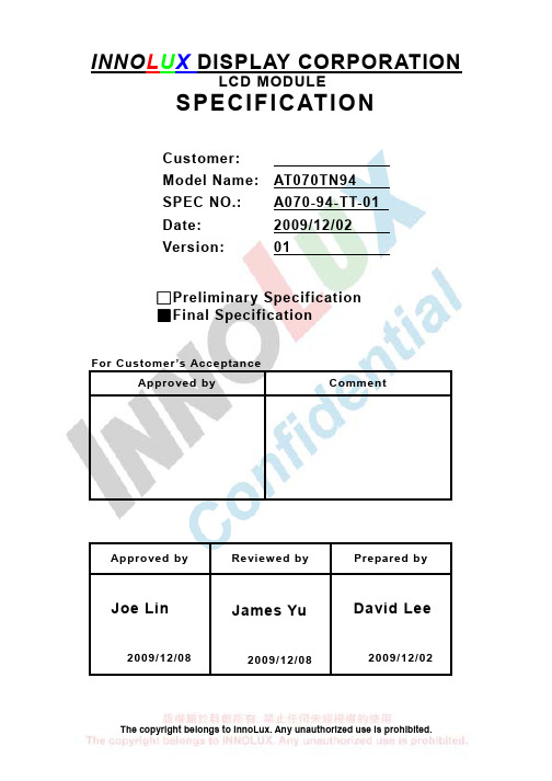
The copyright belongs to InnoLux. Any unauthorized use is prohibited.INNO L U X DISPLAY CORPORATIONLCD MODULESPECIFICATIONCustomer: Model Name: AT070TN94SPEC NO.: A070-94-TT-01 Date: 2009/12/02 Version:01□Preliminary Specification ■Final SpecificationFor Customer ’s AcceptanceApproved byCommentApproved byReviewed by Prepared byJoe Lin2009/12/08James Yu2009/12/08David Lee2009/12/02InnoLux copyright 2004All rights reserved,Copying forbidden.Record of RevisionVersion Revise Date Page ContentPre-Spec.01 2009/07/07 All Initial ReleaseFinal-spec.01 2009/12/02 All The first version final specification.6 Modify V COM to 3.8V(Typ.), 3.6V(Min.) and 4.0V(Max.).9 Add Input Clock and Data Timing Diagram.18 Update the Mechanical Drawing.The copyright belongs to InnoLux. Any unauthorized use is prohibited.I NNO L U XContents1. General Specifications (1)2. Pin Assignment (2)3. Operation Specifications (5)3.1. Absolute Maximum Ratings (5)3.1.1. Typical Operation Conditions (6)3.1.2. Current Consumption (7)3.1.3. Backlight Driving Conditions (7)3.2. Power Sequence (8)3.3. Timing Characteristics (9)3.3.1. AC Electrical Characteristics (9)3.3.2. Input Clock and Data Timing Diagram (9)3.3.3. Timing (10)3.3.4. Data Input Format (11)4. Optical Specifications (12)5. Reliability Test Items (16)6. General Precautions (17)6.1. Safety (17)6.2. Handling (17)6.3. Static Electricity (17)6.4. Storage (17)6.5. Cleaning (17)7. Mechanical Drawing (18)8. Package Drawing (19)8.1. Packaging Material Table (19)8.2. Packaging Quantity (19)8.3. Packaging Drawing (20)The copyright belongs to InnoLux. Any unauthorized use is prohibited.1. General SpecificationsNo. Item Specification Remark1 LCD size 7.0 inch(Diagonal)2 Driver element a-Si TFT active matrix3 Resolution 800 × 3(RGB) × 4804 Display mode Normally White, Transmissive5 Dot pitch 0.0642(W) × 0.1790(H) mm6 Active area 154.08(W) × 85.92(H) mm7 Module size 164.9(W) ×100.0(H) ×5.7(D) mm Note 18 Surface treatment Anti-Glare9 Color arrangement RGB-stripe10 Interface Digital11 Backlight power consumption 1.674W (Typ.)12 Panel power consumption 0.226W (Typ.)13 Weight 150g (Typ.)Note 1: Refer to Mechanical Drawing.2. Pin AssignmentFPC Connector is used for the module electronics interface. The recommended model is FH12A-50S-0.5SH manufactured by Hirose.Pin No. Symbol I/O Function Remark1 V LED+P Power for LED backlight (Anode)2 V LED+P Power for LED backlight (Anode)3 V LED-P Power for LED backlight (Cathode)4 V LED-P Power for LED backlight (Cathode)5 GND P Power ground6 V COM I Common voltage7 DV DD P Power for Digital Circuit8 MODE I DE/SYNC mode select Note 19 DE I Data Input Enable10 VS I Vertical Sync Input11 HS I Horizontal Sync Input12 B7 I Blue data(MSB)13 B6 I Blue data14 B5 I Blue data15 B4 I Blue data16 B3 I Blue data17 B2 I Blue data18 B1 I Blue data Note 219 B0 I Blue data(LSB) Note 220 G7 I Green data(MSB)21 G6 I Green data22 G5 I Green data23 G4 I Green data24 G3 I Green data25 G2 I Green data26 G1 I Green data Note 227 G0 I Green data(LSB) Note 228 R7 I Red data(MSB)29 R6 I Red data30 R5 I Red data31 R4 I Red data32 R3 I Red data33 R2 I Red data34 R1 I Red data Note 235 R0 I Red data(LSB) Note 236 GND P Power Ground37 DCLK I Sample clock Note 338 GND P Power Ground39 L/R I Left / right selection Note 4,540 U/D I Up/down selection Note 4,541 V GH P Gate ON Voltage42 V GL P Gate OFF Voltage43 AV DD P Power for Analog Circuit44 RESET I Global reset pin. Note 645 NC - No connection46 V COM I Common Voltage47 DITHB I Dithering function Note 748 GND P Power Ground49 NC - No connection50 NC - No connectionI: input, O: output, P: PowerNote 1: DE/SYNC mode select. Normally pull high.When select DE mode, MODE=”1”, VS and HS must pull high.When select SYNC mode,MODE= ”0”, DE must be grounded.Note 2: When input 18 bits RGB data, the two low bits of R,G and B data must be grounded.Note 3:Data shall be latched at the falling edge of DCLK.Note 4: Selection of scanning modeSetting of scan control inputU/D L/R Scanning direction GND DV DD Up to down, left to right DV DD GND Down to up, right to left GND GND Up to down, right to left DV DDDV DDDown to up, left to rightNote 5: Definition of scanning direction. Refer to the figure as below:Note 6: Global reset pin. Active low to enter reset state. Suggest to connect with an RCreset circuit for stability. Normally pull high.Note 7: Dithering function enable control, normally pull high. When DITHB=”1”,Disable internal dithering function, When DITHB=”0”,Enable internal dithering function,RightLeft DownUp3. Operation Specifications3.1. Absolute Maximum Ratings(Note 1)ValuesItem SymbolMin. Max.Unit RemarkDV DD -0.3 5.0 VAV DD 6.5 13.5 VV GH -0.3 40.0 VV GL -20.0 0.3 V Power voltageV GH-V GL- 40.0 V Operation Temperature T OP -30 85 ℃Storage Temperature T ST-30 85 ℃LED Reverse Voltage V R- 1.2 VEach LEDNote 2 LED Forward Current I F- 25 mA Each LEDNote 1: The absolute maximum rating values of this product are not allowed to be exceeded at any times. Should a module be used with any of the absolute maximum ratingsexceeded, the characteristics of the module may not be recovered, or in an extremecase, the module may be permanently destroyed.Note 2: V R Conditions: Zener Diode 20mA3.1.1. Typical Operation Conditions( Note 1)ValuesUnit Remark Item SymbolMin. Typ. Max.DV DD 3.0 3.3 3.6 V Note 2AV DD 10.2 10.4 10.6 VPower voltageV GH 15.3 16.0 16.7 VV GL -7.7 -7.0 -6.3 VInput signal voltage V COM 3.6 3.8 4.0 VInput logic high voltage V IH 0.7 DV DD - DV DD VNote 3 Input logic low voltage V IL 0 - 0.3 DV DD VNote 1: Be sure to apply DV DD and V GL to the LCD first, and then apply V GH.Note 2: DV DD setting should match the signals output voltage (refer to Note 3) of customer’s system board.Note 3: DCLK,HS,VS,RESET,U/D, L/R,DE,R0~R7,G0~G7,B0~B7,MODE,DITHB.3.1.2. Current ConsumptionValuesItem SymbolMin. Typ. Max.Unit RemarkI GH - 0.2 1.0 mA V GH =16.0VI GL - 0.2 1.0 mA V GL = -7.0V IDV DD - 4.0 10 mA DV DD =3.3VCurrent for DriverIAV DD - 20 50 mA AV DD =10.4V3.1.3. Backlight Driving ConditionsValuesItem SymbolMin. Typ. Max.Unit Remark Voltage for LED backlight V L 8.4 9.3 10.2 V Note 1 Current for LED backlight I L 170 180 200 mALED life time - 20,000 - - Hr Note 2Note 1: The LED Supply Voltage is defined by the number of LED at Ta=25℃ andI L =180mA.Note 2: The “LED life time” is defined as the module brightness decrease to 50% original brightness at Ta=25℃ and I L =180mA. The LED lifetime could be decreased ifoperating I L is lager than 180mA.3.2. Power Sequencea. Power on:Note: Data include R0~R7, B0~B7, GO~G7, U/D, L/R, DCLK, HS,VS,DE.DV DD→VGL→AVDD→VGH→Data→B/LB/L→Data→VGH→AVDD→VGL→DV DD3.3. Timing Characteristics3.3.1. AC Electrical CharacteristicsValuesItem SymbolMin. Typ. Max.Unit Remark HS setup time T hst8 - - nsHS hold time T hhd 8 - - nsVS setup time T vst8 - - nsVS hold time T vhd8 - - nsData setup time T dsu8 - - nsData hole time T dhd8 - - nsDE setup time T esu 8 - - nsDE hole time T ehd8 - - nsDV DD Power On Slew rate T POR - - 20 ms From 0 to 90% DV DDRESET pulse width T Rst 1 - - ms DCLK cycle time T coh 20 - - ns DCLK pulse duty T cwh 40 50 60 %3.3.2. Input Clock and Data Timing Diagram3.3.3. TimingValuesUnit Remark Item SymbolMin. Typ. Max.Horizontal Display Area thd- 800 - DCLKDCLK Frequency fclk26.4 33.3 46.8 MHzOne Horizontal Line th862 1056 1200 DCLKHS pulse width thpw 1 - 40 DCLKHS Blanking thb46 46 46 DCLKHS Front Porch thfp 16 210 354 DCLKValuesItem SymbolUnit RemarkMin. Typ. Max.Vertical Display Area tvd- 480 - THVS period time tv 510 525 650 THVS pulse width tvpw 1 - 20 THVS Blanking tvb23 23 23 THVS Front Porch tvfp7 22 147 TH3.3.4. Data Input Format4. Optical SpecificationsValuesItem Symbol ConditionMin. Typ. Max.Unit RemarkθL Φ=180°(9 o’clock) 60 70 -θRΦ=0°(3 o’clock) 60 70 -θTΦ=90°(12 o’clock) 40 50 -Viewing angle(CR≥ 10)θBΦ=270°(6 o’clock) 60 70 -degree Note 1T ON - 10 20 msec Note 3 Response timeT OFF - 15 30 msec Note 3 Contrast ratio CR 400 500 - - Note 4W X 0.26 0.31 0.36 -Color chromaticityW Y 0.28 0.33 0.38 -Note 2Note 5Note 6 Luminance L 320 400 - cd/m² Note 6 LuminanceuniformityY UNormalθ=Φ=0°70 75 - % Note 7Test Conditions:1. DV DD=3.3V, I L=180mA (Backlight current), the ambient temperature is 25℃.2. The test systems refer to Note 2.Note 1: Definition of viewing angle rangeFig. 4-1 Definition of viewing angleNote 2: Definition of optical measurement system.The optical characteristics should be measured in dark room. After 30 minutesoperation, the optical properties are measured at the center point of the LCD screen. (Response time is measured by Photo detector TOPCON BM-7, other items are measured by BM-5A/Field of view: 1° /Height: 500mm.)Normal line θ=Φ=0°Photo detectorΦ=90°12 o’clock directionΦ=270° 6 o’clock directionΦ=0°Φ=180°Active Area500mmLCMNormal line θ=Φ=0°Φ=90°12 o’clock directionΦ=270°6 o’clock directionΦ=0°Φ=180°Active AreaθLθTθBθRLCMNote 3: Definition of Response timeThe response time is defined as the LCD optical switching time interval between“White” state and “Black” state. Rise time (T ON) is the time between photo detector output intensity changed from 90% to 10%. And fall time (T OFF) is the timebetween photo detector output intensity changed from 10% to 90%.Fig. 4-3 Definition of response timeNote 4: Definition of contrast ratiostateBlack""theonLCDwhenmeasuredLuminancestateWhite""theonLCDwhenmeasuredLuminance(CR)ratioContrast=Note 5: Definition of color chromaticity (CIE1931)Color coordinates measured at center point of LCD.Note 6: All input terminals LCD panel must be ground while measuring the center area of the panel.The LED driving condition is I L=180mA .90%10%0%Photodetectoroutput(Relativevalue)ONTWhite (TFT OFF) Black (TFT ON) White (TFT OFF)Note 7:Definition of Luminance UniformityActive area is divided into 9 measuring areas (Refer to Fig. 4-4 ).Every measuring point is placed at the center of each measuring area.maxminBB(Yu)UniformityLuminance=L-------Active area length W----- Active area widthWW/3W/3W/6L/3L/3L/6LFig. 4-4 Definition of measuring pointsB max: The measured maximum luminance of all measurement position.B min: The measured minimum luminance of all measurement position.5. Reliability Test Items(Note3)Item Test Conditions Remark High Temperature Storage Ta = 85℃240hrs Note 1,Note 4 Low Temperature Storage Ta = -30℃240hrs Note 1,Note 4 High Temperature Operation Ts = 85℃240hrs Note 2,Note 4 Low Temperature Operation Ta = -30℃240hrs Note 1,Note 4 Operate at High Temperatureand Humidity+60℃, 90%RH 240hrs Note 4Thermal Shock -30℃/30 min ~ +85℃/30 min for a total 100cycles, Start with cold temperature and endwith high temperature.Note 4Vibration Test Frequency range:10~55Hz Stroke:1.5mmSweep:10Hz~55Hz~10Hz2 hours for each direction of X. Y. Z.(6 hours for total)Mechanical Shock 100G 6ms,±X, ±Y, ±Z 3 times for each directionPackage Vibration Test Random Vibration :0.015G*G/Hz from 5-200HZ, -6dB/Octave from 200-500HZ2 hours for each direction of X. Y. Z.(6 hours for total)Package Drop Test Height:60 cm1 corner, 3 edges, 6 surfacesElectro Static Discharge ± 2KV, Human Body Mode, 100pF/1500ΩNote 1: Ta is the ambient temperature of samples.Note 2: Ts is the temperature of panel’s surface.Note 3: In the standard condition, there shall be no practical problem that may affect the display function. After the reliability test, the product only guarantees operation,but don’t guarantee all of the cosmetic specification.Note 4: Before cosmetic and function test, the product must have enough recovery time, at least 2 hours at room temperature.6. General Precautions6.1. SafetyLiquid crystal is poisonous. Do not put it in your mouth. If liquid crystal touches your skin or clothes, wash it off immediately by using soap and water.6.2. Handling1. The LCD panel is plate glass. Do not subject the panel to mechanical shock or toexcessive force on its surface.2. The polarizer attached to the display is easily damaged. Please handle it carefullyto avoid scratch or other damages.3. To avoid contamination on the display surface, do not touch the module surfacewith bare hands.4. Keep a space so that the LCD panels do not touch other components.5. Put cover board such as acrylic board on the surface of LCD panel to protect panelfrom damages.6. Transparent electrodes may be disconnected if you use the LCD panel underenvironmental conditions where the condensation of dew occurs.7. Do not leave module in direct sunlight to avoid malfunction of the ICs.6.3. Static Electricity1. Be sure to ground module before turning on power or operating module.2. Do not apply voltage which exceeds the absolute maximum rating value.6.4. Storage1. Store the module in a dark room where must keep at 25±10℃ and 65%RH or less.2. Do not store the module in surroundings containing organic solvent or corrosivegas.3. Store the module in an anti-electrostatic container or bag.6.5. Cleaning1. Do not wipe the polarizer with dry cloth. It might cause scratch.2. Only use a soft sloth with IPA to wipe the polarizer, other chemicals mightpermanent damage to the polarizer.7. Mechanical Drawing8. Package Drawing8.1. Packaging Material TableNo. ItemModel(Material)Dimensions(mm)UnitWeight(kg)Quantity Remark1 LCMModuleAT070TN94 164.9 × 100.0 × 5.7 0.150 50pcs2 Partition BC Corrugatedpaper512 × 349 × 226 1.466 1set3 CorrugatedPaperB Corrugatedpaper510 × 350 0.071 4pcs4 CorrugatedBarB Corrugatedpaper512 × 11 × 3 0.046 4pcs5 Dust-ProofBagPE 700 × 530 0.048 1pcs6 A/S Bag PE 180 × 133 × 0.2 0.002 50pcs7 Carton Corrugatedpaper530 × 355 × 255 1.100 1pcs8 Total weight 10.682 kg± 5%8.2. Packaging QuantityTotal LCM quantity in Carton: no. of Partition 2 Rows × quantity per Row 25 = 508.3. Packaging Drawing。
JHD 新品介绍(7寸TFT控制方案)9-25

深圳晶华显示器材有限公司
SHENZHEN JINGHUA DISPLAYS CO., LTD.
SINCE 1987 INNOVATION
3.2, 背光驱动电路
3.2.1 内置背光驱动IC,实现恒流驱动,延长背光寿命. 3.2.2 背光开关可控:客户可根据自身需要实现背光的开关控制. 3.2.3 背光亮度可调:带PWM调节功能,客户只需对PWM寄存器设置相应的参数即 能灵活实现背光的PWM亮度调节功能.
深圳晶华显示器材有限公司
SHENZHEN JINGHUA DISPLAYS CO. Nhomakorabea LTD.
SINCE 1987 INNOVATION
二,产品外观图
给用户的标准 TFT接口
USB接口
产品正面与原标准7寸屏尺寸相当
产品背面有控制板:提供给用户的有标准TFT驱动接口 和USB接口,用户可选其中任何一种来驱动
SD/TF卡 槽
深圳晶华显示器材有限公司
SHENZHEN JINGHUA DISPLAYS CO., LTD.
SINCE 1987 INNOVATION
3.6 触摸屏驱动
3.6.1 内置四线电阻触摸屏驱动电路,可根据用户的需求来选择是否增加此部分电路。 3.6.2 最高支持12 bit ADC,能满足大部分四线电阻触摸屏的精度.
SINCE 1987 INNOVATION
JHD新产品推介
深圳晶华显示器材有限公司
SHENZHEN JINGHUA DISPLAYS CO., LTD.
SINCE 1987 INNOVATION
一,产品概述:
1.1 7寸TFT+TFT控制器+MCU(可选)架构 ,可以满足客户端灵活选择相应的驱动方案; 1.2. MCU内置USB驱动,支持USB2.0协议,向下兼容; 1.3. 预留32PIN标准的TFT MCU驱动接口,支持I8080和M6800时序; 1.4. 可灵活选择电源:外部电源或USB供电,如果选择 外部电源, 有+5V和+3.3V可供选择; 1.5. 内部已经集成LCD所有驱动电压,无需客户设计升压电路, 用户只需提供LCD控制器所需的信号就能正常驱动点亮TFT屏; 1.6. 背光驱动电压可选内部产生也可用户自己提供; 1.7. 内部集成通用SD卡作为存储媒介,可满足用户大容量存储; 1.8. 预留触摸屏驱动电路,可根据用户需求增加触摸屏驱动电路; 1.9. 可用于工控及其它终端显示领域。
信立科技XL7070s电阻式触摸屏使用手册_V1.1

XL7070s 触摸屏使用手册1 产品概述正视图背视图XL7070s是一款以先进的Cortex-A8 CPU为核心(主频1.0G)的高性能嵌入式一体化人机界面。
该产品设计采用7英寸高亮LED液晶显示器(分辨率800*480),四线电阻式触摸屏(分辨率4096*4096)。
支持WIN CE6.0, 同时预装Corware V2.9.8工业组态软件。
·液晶屏: 7寸TFT液晶屏、LED背光、颜色65535·分辨率:800*480·显示亮度:350cd/m2· C P U:ARM Cortex A8,主频1.0G·内存:256M DDRII RAM·触摸屏:四线电阻式,点动100万次以上·存储设备:256M NAND FLASH·SD卡扩展:可选,最大可扩展32G·接口:1*RS232、1*RS485、1*USB 2.0、1*LAN ·实时时钟:有·蜂鸣器:有·重量: 1.04 Kg·防护等级: IP 65(前面板)·耐压测试: 500V AC 1分钟·抗干扰性:工频磁场干扰度5级,磁场强度100A/m 2 外观尺寸开孔图3 挂钩安装说明1.将TPC放置于安装槽内2.将挂钩勾脚放于TPC侧面安装孔内,用十字起拧紧螺丝,安装完成。
4 电源连接接线步骤:步骤1:将DC24V电源线剥线后插入电源插头接线端子中;步骤2:使用一字螺丝刀将电源插头螺丝锁紧;步骤3:将电源插头插入产品的电源插座。
电源插头示意图及引脚定义如下:5 外部接口5.1 接口说明LAN USB COM1/2 电源5.2 串口引脚定义5.3 TPC与PLC的连接TPC Siemens S7-200系列PPI 9针D形母头9针D形公头TPC Omron C/CV/CS/CJ/CP系列HostLink 9针D形母头9针D形公头PORT口接口PIN引脚定义COM COM12 RS232 RXD3 RS232 TXD5 GNDCOM27 RS485 +8 RS485 -7 RS485 +8 RS485 - 8 D -3 D +2 RX 2 TX2-5k 电阻,推荐3.3K 2-5k 电阻,推荐3.3KTPC 三菱电机FX 系列编程口 9针 D 形母头 8针 Din 圆形公头6 工程下载6.1 工程下载方法一:6.1.1 硬件连接连接方式:网线连接6.1.2 启动TPC使用24V 直流电源给TPC 供电,开机启动后屏幕出现“CORTEK ”logo ,此时不需要任何操作,系统将自动进入工程运行界面。
XH70745B7寸电容触摸屏规格书-杭州旭虹科技有限公司)
边沿区域漏光宽度≤0.25mm
★
边沿区域漏光宽度>0.25mm
★
ITO表面不允许有不可清洁处理的脏
污、水印
★
无法清洁的脏污按点状不良判定
★
FPC 缺陷
凹痕,针孔 a≤w/3
★
开路/划伤线路/裂开
★
氧化,污染
★
FPC 折伤
FPC 折伤/压伤 ;死折(锐角折痕)不
允许,锐角凸起
★
6. Notice 注意事项
NO PART OF THIS SPECIFICATION MAY BE REPRODUCED OR TRANSMITTED IN ANY FORM OR BY ANY MEANS WITHOUT THE EXPRESSED WRITTEN PERMISSION OF WGJ.
工业液晶屏http://www.hzxuhong.com
80ºC,240hrs -30ºC,240hrs 60ºC/90% RH,240hrs
70ºC,24hrs -20 ºC,24hrs 60ºC/90%RH,24hrs -30 ~ 80℃, 60 Mins/cycle , Total 10
Cycles
4. Touch panel description 触摸屏功能描述
Date 日期 Ver.版
Hangzhou Xu Hong Technology Co.,Ltd
History of Version 变更记录
Description 描述
Page 页 Design by 变更人
2016-02-27
A0 在 XH70745A-GDA-A1 基础上更改盖板
10/10
LLL
2016-03-15
7 寸 TFT显示屏规格书
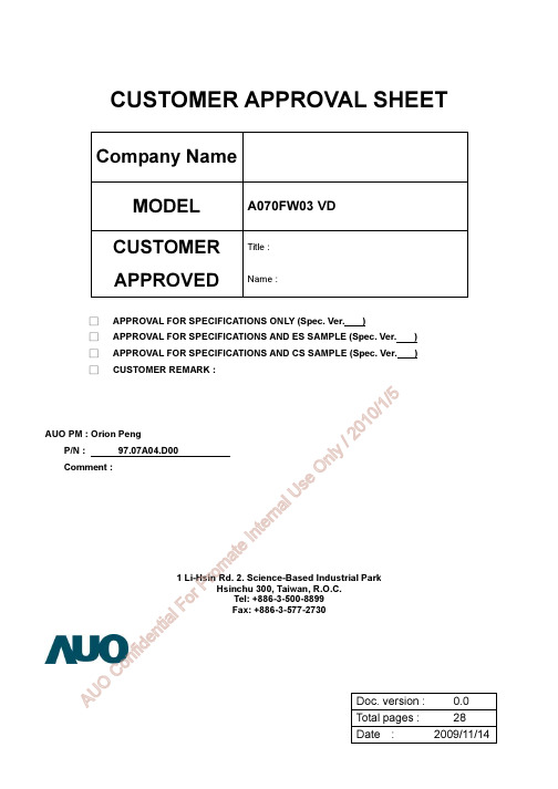
CUSTOMER APPROVAL SHEETCompany NameMODELA070FW03 VDCUSTOMERAPPROVEDTitle : Name :□ APPROVAL FOR SPECIFICATIONS ONLY (Spec. Ver. )□ APPROVAL FOR SPECIFICATIONS AND ES SAMPLE (Spec. Ver. ) □ APPROVAL FOR SPECIFICATIONS AND CS SAMPLE (Spec. Ver. ) □CUSTOMER REMARK :AUO PM : Orion PengP/N : 97.07A04.D00Comment :1 Li-Hsin Rd. 2. Science-Based Industrial ParkHsinchu 300, Taiwan, R.O.C.Tel: +886-3-500-8899 Fax: +886-3-577-2730Doc. version : 0.0 Total pages : 28A UOCo n fi de n ti a lF or Pr om a t eI nt er na l Us eOn l y / 2010/1/5Product Specification7.0" COLOR TFT-LCD MODULEModel Name :A070FW03 VDPlanned Lifetime: From 2009/Dec To2011/DecPhase-out Control:From 2011/Jul To 2011/DecEOL Schedule:2011/Jul< >Preliminary Specification < >Final SpecificationNote: The content of this specification is subject to change.© 2009 AU Optronics All Rights Reserved, Do Not Copy.A UOCo n fi de n ti a lF or Pr om a t eI nt er na l Us eOn l y / 2010/1/5Page:1/28Record of RevisionVersion Revise Date Page Content0.0 2009/03/10All First DraftA UOCo n fi de n ti a lF or Pr om a t eI nt er na l Us eOn l y / 2010/1/5Page:2/28ContentsA. General Information.....................................................................................................................................3B.Outline Dimension (4)1. TFT-LCD Module – Front View....................................................................................................................42. TFT-LCD Module – Rear View....................................................................................................................5 C.Electrical Specifications .............................................................................................................................6 1. TFT LCD Panel Pin Assignment .................................................................................................................6 2. Backlight Pin Assignment............................................................................................................................7 3. Absolute Maximum Ratings.........................................................................................................................7 3. Electrical DC Characteristics.......................................................................................................................8 4. Electrical AC Characteristics.....................................................................................................................10 6. Power On/Off Characteristics....................................................................................................................17 D. Optical Specification .................................................................................................................................18 E. Reliability Test Items .................................................................................................................................21 F.Packing and Marking.................................................................................................................................24 1. Packing Form............................................................................................................................................24 2. Module/Panel Label Information ...............................................................................................................25 3. Carton Label Information...........................................................................................................................25 G.Precautions (26)A UOCo n fi de n ti a lF or Pr om a t eI nt er na l Us eOn l y / 2010/1/5Page:3/28A. General InformationThis product is for portable DVD and digital photo frame application. NO. ItemUnit Specification Remark1 Screen Sizeinch 7.0(Diagonal)2 Display Resolution dot480RGB(W)×234(H)3 Overall Dimensionmm 164.9 (W)×100(H)×5.7(D) Note 1 4 Active Area mm154.08(W)×86.58(H) 5 Pixel Pitchmm 0.107(W)×0.370(H)6 Color Configuration --R. G. B. Stripe Note 2 7 NTSC Ratio% 48%8 Display Mode -- Normally White 9Panel surface Treatment -- Anti-Glare, 3H10 Weight g TBD 11 LCD Module Power ConsumptionW 2.212 Viewing direction6 o’clock (gray inversion)Note 1: Not include blacklight cable and FPC. Refer next page to get further information. Note 2: Below figure shows dot stripe arrangement.( 1………………………..234)A UOCo n fi de n ti a lF or Pr om aPage:4/28ALL RIGHTS STRICTLY RESERVED. ANY PORTION OF THIS PAPER SHALL NOT BE REPRODUCED, COPIED, OR TRANSFORMED TO ANY OTHER FORMSWITHOUT PERMISSION FROM AU OPTRONICS CORP.B. Outline Dimension (D00)1. TFT-LCD Module – Front ViewA UOPage:5/28ALL RIGHTS STRICTLY RESERVED. ANY PORTION OF THIS PAPER SHALL NOT BE REPRODUCED, COPIED, OR TRANSFORMED TO ANY OTHER FORMSWITHOUT PERMISSION FROM AU OPTRONICS CORP.2. TFT-LCD Module – Rear ViewA UPage:6/28C. Electrical Specifications1. TFT LCD Panel Pin AssignmentPin no Symbol I/O DescriptionRemark1 GND - Ground for logic circuit2 V CC I Supply voltage of logic control circuit for scan driver3 V GL I Negative power for scan driver4 V GH IPositive power for scan driver5 STVR I/O Vertical start pulse Note 16 STVL I/O Vertical start pulse Note 17 CKV I Shift clock input for scan driver 8 U/D I UP/DOWN scan control input Note 1,29 OEV I Output enable input for scan driver 10 VCOM I Common electrode driving signal 11 VCOM I Common electrode driving signal12 L/R I LEFT/RIGHT scan control input Note 1,213 MOD I Sequential sampling and simultaneous sampling setting14 OEH IOutput enable input for data driver15 STHL I/O Start pulse for horizontal scan lineNote 1 16 STHR I/O Start pulse for horizontal scan lineNote 1 17 CPH3 I Sampling and shifting clock pulse for data driver18 CPH2 I Sampling and shifting clock pulse for data driver19 CPH1 I Sampling and shifting clock pulse for data driver20 V CC I Supply voltage of logic control circuit for data driver21 GND - Ground for logic circuit22 VRIAlternated video signal input(Red) 23 VGI Alternated video signal input(Green) 24VBI Alternated video signal input(Blue)25 AV DD I Supply voltage for analog circuit 26AV SS-Ground for analog circuitA UOCo n fi de n ti a lF or Pr om a t eI nt er na l Us eOn l y / 2010/1/5Page:7/28I: Input pin; P: Power pin; G: Ground pin; C: capacitor pinRefer to figure as below:Pin26 Pin12. Backlight Pin AssignmentRecommended connector : E&T H201K-P020N-02BPin no Symbol I/O Description Remark1 VLEDPLED power supply2GNDLEDP LED ground3. Absolute Maximum RatingsItemSymbol Condition Min. Max. Unit RemarkV CCGND=0-0.3 7 V AV DD AGND=0-0.3 7VV GH -0.3 18 V V GL GND=0-15 0.3 V Power voltageV GH -V GL-33VV i-0.3 AV DD +0.3 VNote 3 V I-0.3 V CC +0.3 V Note 4 Input signal voltageVCOM-2.9 7.5 VNote 1: Functional operation should be restricted under ambient temperature (25℃).Note 2: Maximum ratings are those values beyond which damages to the device may occur. Functionaloperation should be restricted to the limits in the Electrical Characteristics chapter.Note 3: VR, VG, VB.Note 4: STHL, STHR, OEH, LRC, CPH1~CPH3, STVD, STVU, OEV, CKV, UDC, MODA UOCo n fi de n ti a lF or Pr om a t eI nt er na l Us eOn l y / 2010/1/5Page:8/283. Electrical DC Characteristicsa. Typical Operation Condition (AGND =GND = 0V)ItemSymbol Min. Typ. Max. Unit Remark V CC3 3.3 5.5 VDigital powerAV DD4.5 55.5 V Analog PowerV GH 14.3 15 15.7 V Positive power supply for gate driver Power VoltageVGL-10.5 -10 -9.5 V Negative power supply for gate driverV iA 0.4 - AV DD -0.4V Refer to Horizontal timing V iAC - 4- V AC component Video signal amplitude(VR,VG,VB) V iDC -AV DD /2 -VDC componentH LevelVIH 0.8xVCC - VCC VInputSignal Voltage L Level VIL GND - 0.2xVC VNote 1. V CAC 3.5 5.6 6.5 VAC component Gamma referencevoltageV CDC1.41.72.0VDC component Note 1: STHL, STHR, OEH, LRC, CPH1~CPH3, STVD, STVU, OEV, CKV, UDC, MOD.Note2: Must follow power On/Off Sequence.Note 3: If input signal amplitude is 3.3V, recommend value for Vcc is 3.3VIf input signal amplitude is 5V, recommend value for Vcc is 5Vb. Current Consumption (AGND=GND=0V)ParameterSymbol ConditionMin. Typ. Max. Unit RemarkInput current for V GH I GH V GH =15V- 0.12 1.0 m A Input current for V Gl I GL V Gl =-10V- 0.15 1.0 mA Input current for Vcc I CC DV CC =3.3- 2 6.0 mA Input current for Avdd I DDAV DD =5V-5.330mAA UOCo n fi de n ti a lF or Pr om a t eI nt er na l Us eOn l y / 2010/1/5Page:9/28c. Backlight Driving ConditionsThe backlight (LED module, Note 1) is suggested to drive by constant current with typical value.ParameterSymbol Min. Typ. Max. Unit Remark LED light bar CurrentI L-- 200 -- mABL Power ConsumptionP BL --2.1 --WNote 1 LED Life TimeL L 10,000 ---- Hr Note 2, 3Note 1: The LED driving condition is defined for LED module (24 LED). The voltage range will be 8.7 to 11.6V based on suggested driving current set as 200mA .Note 2: Define “LED Lifetime”: brightness is decreased to 50% of the initial value. LED Lifetime isrestricted under normal condition, ambient temperature = 25℃ and LED lightbar current =200mA .Note 3: If it uses larger LED lightbar voltage more than 200mA , it maybe decreases the LED lifetime.A UOCo n fi de n ti a lF or Pr om a t eI nt er na l Us eOn l y / 2Page:10/284. Electrical AC Characteristicsa. Signal AC CharacteristicsParameterSymbol Min. Typ. Max. Unit. Remark Clock cycle time t CPH100 103 107 ns CPH1 CPH pulse duty t CWH 405060%CPH1CPH pulse delay t C12 30 t CPH /3 t CPH /2 ns CPH1STH setup time t SUH 20 - - ns STHR,STHL STH hold time t HDH 20- - ns STHR,STHL STH pulse width t STH 1 t CPH STHR,STHL STH period t H 61.8 63.7 66.1 μs STHR,STHL OEH pulse width t OEH 1 - - t CPH OEH (Note 1)Sample and hold disable timet DIS1 1 - - t CPH Note 2 OEV pulse width t OEV 2.0 3.4 6.5 μs OEV CKV pulse width t CKV 1.0 3.1 4.68 μs CKV Clean enable timet DIS2 1.0- 1 t OEVμs Note 3 Horizontal display start t SH 1t CPH Horizontal display timing ranget DH 480t CPH STV setup time t SUV 400 -- ns STVU, STVD STV hold time t HDV 400 -- ns STVU, STVD STV pulse width t STV - -1t H STVU, STVDVertical display start t SV 3t H Vertical display timing ranget DV 234 t HVCOM rising time t rCOM - 5 μs VCOM falling time t fCOM- 5 μs VCOM delay time t DCOM 2 - - μs TFT charging time t ch 55 - - μs Output time delay t del 3 - - μs Setup time of analog VR/VG/VBt asu 60 - - ns Hold time of analog VR/VG/VBt ahd 40 - - ns Frame rate5060-HzNote 1: The maximum pulse width of OEH should refer to the minimum of tDIS1 and the hsyncback porch.Note 2: t DIS1 is time difference between OEH and STHL.Note 3: t DIS2 is time difference between OEV and CKVA UOCo n fi de n ti a lF or Pr om a t eI nt er na l Us eOn l y / 2010/1/5Sampling clock timingVersion:0.0Page: 15/28ALL RIGHTS STRICTLY RESERVED. ANY PORTION OF THIS PAPER SHALL NOT BE REPRODUCED, COPIED, OR TRANSFORMED TO ANY OTHER FORMS WITHOUT PERMISSION FROM AU OPTRONICS CORP.Vertical timing (From up to down)a lUs e On ly / 2010/1/5Version:0.0Page: 16/28ALL RIGHTS STRICTLY RESERVED. ANY PORTION OF THIS PAPER SHALL NOT BE REPRODUCED, COPIED, OR TRANSFORMED TO ANY OTHER FORMS WITHOUT PERMISSION FROM AU OPTRONICS CORP.Page: 17/28 6. Power On/Off CharacteristicsPower OnPage:18/28D. Optical SpecificationAll optical specification is measured under typical condition (Note 1, 2)Item Symbol Condition Min. Typ. Max. Unit Remark Response TimeRise FallTr Tfθ=0°-- --12 1824 36ms ms Note 3 Contrast ratioCRAt optimizedviewing angle 300 400 -- Note 4TopBottom LeftViewing AngleRight 30 50 50 5040 65 65 65 -- -- -- -- deg. Note 5Brightness Y Lθ=0° 320 400 -- cd/m 2 Note 6 X θ=0° 0.25 0.30 0.35 ChromaticityWhiteY θ=0° 0.27 0.32 0.37 UniformityΔY L%7075 -- %Note 7Note 1: Ambient temperature =25℃, and LED lightbar current I L = 200 mA . To be measured in the dark room.Note 2: To be measured on the center area of panel with a viewing cone of 1° by Topcon luminance meterBM-5A, after 15 minutes operation.Note 3: Definition of response time:The output signals of photo detector are measured when the input signals are changed from“black” to “white”(falling time) and from “white” to “black”(rising time), respectively.The response time is defined as the time interval between the 10% and 90% of amplitudes.Refer to figure as below.A UOCo n fi de n ti a lF or Pr om 1/5Note 4.Definition of contrast ratio:Contrast ratio is calculated with the following formula.statusBlack"" at is LCD when output detector Photo statusWhite"" at is LCD when output detector Photo (CR) ratio Contrast =Note 5. Definition of viewing angle, θ, Refer to figure as below.Note 6. Measured at the center area of the panel when all the input terminals of LCD panel areelectrically opened.Note 7: Luminance Uniformity of these 9 points is defined as below:A UOCo n fi de n ti a lF or Pr om a t eI nt er nA UOCo n fi de n ti a lF or Pr om a t eI nt er na l Us eOn l y / 2010/1/5Page:21/28E. Reliability Test ItemsNo. Test itemsConditions Remark1 High Temperature Storage240Hrs2 Low Temperature Storage Ta= -2240Hrs3 High Ttemperature Operation Tp240Hrs4 Low Temperature Operation Ta= -1 240Hrs5 High Temperature & High HumidityTp= 580% RH 240Hrs Operation6 Heat Shock -20d/1hr~70d/1hr judge 50cyclesNon-operation7 Electrostatic DischargeContact = ± 4 kV, class B Air = ± 8 kV, class BNote 4 8Image Sticking25, 4hrsNote 5Frequency range : 10~55HzStoke: 1.5mmSweep: 10 Hz ~55 Hz 2 hours for each direction of X,Y,Z9Vibration4 hours for Y directionNon-operationJIS C7021, A-10condition A : 15 minutes10 Mechanical Shock100G . 6ms, ±X,±Y,±Z3 times for each directionNon-operation JIS C7021,A-7condition C 11 Vibration (With Carton)Random vibration:0.015G 2/Hz from 5~200Hz–6dB/Octave from 200~500Hz IEC 68-3412 Drop (With Carton)Height: 60cm1 corner, 3 edges, 6 surfaces13 Pressure5kg, 5sec Note 6Note 1: Ta: Ambient Temperature. Tp: Panel Surface TemperatureNote 2: In the standard conditions, there is not display function NG issue occurred. All the cosmeticspecification is judged before the reliability stress.Note 3: All the cosmetic specification is judged before the reliability stress.Note 4 : All test techniques follow IEC6100-4-2 standard.A UOCo n fi de n ti a lF or Pr om a t eI nt er na l Us eOn l y / 2010/1/5Page:22/28Contact Discharge :330Ω, 150pF, 1sec, 8 point, 25times/pointgray pattern. After 20 minutes, the mura is less than JND 2.5Note 6: The panel is tested as figure. The jig is ψ10 mm made by Cu with rubber and the loadingspeed is 3mm/min on position 1~5. After the condition, no glass crack will be found and panelfunction check is OK.( no guarantee LC mura 、LC bubble)A UOCo n fi de n ti a lF or Pr om a t eI nt eUs eOn l y / 201Page:23/28A UOCo n fi de n ti a lF or Pr om a t eI nt er na l Us eOn l y / 2010/1/5Page:24/28F. Packing and Marking1. Packing FormA UOCo n fi de n ti a lF or Pn l y2. Module/Panel Label InformationThe module/panel (collectively called as the “Product”) will be attached with a label of Shipping Numberwhich represents the identification of the Product at a specific location. Refer to the Product outline drawing for detailed location and size of the label. The label is composed of a 22-digit serial number and printed with code128 with the following definition:Example:501M06ZL06123456781Z05: Product Manufacturing Week Code: WK50 Product Version: Version 1 Product Manufactuing Factory: M063. Carton Label InformationThe packing carton will be attached with a carton label where packing Q’ty, AUO Model Name, AUO PartNumber, Customer Part Number (Optional) and a series of Carton Number in 13 or 14 digits are printed. TheCarton Number is apparing in the following format:Refer to the drawing of packing format for the location and size of the carton label.A UOCo n fi de n ti a lF or Pr om a t eI nt er na l Us eOn l y / 2010/1/5G. Precautions1. Do not twist or bend the module and prevent the unsuitable external force for display module during assembly.2. Adopt measures for good heat radiation. Be sure to use the module with in the specified temperature.3. Avoid dust or oil mist during assembly.4. Follow the correct power sequence while operating. Do not apply the invalid signal, otherwise, it will cause improper shut down and damage the module.5. Less EMI: it will be more safety and less noise.6. Please operate module in suitable temperature. The response time & brightness will drift by different temperature.7. Avoid to display the fixed pattern (exclude the white pattern) in a long period, otherwise, it will cause image sticking.8. Be sure to turn off the power when connecting or disconnecting the circuit. 9. Polarizer scratches easily, please handle it carefully. 10. Display surface never likes dirt or stains.11. A dewdrop may lead to destruction. Please wipe off any moisture before using module.12. Sudden temperature changes cause condensation, and it will cause polarizer damaged.13. High temperature and humidity may degrade performance. Please do not expose the module to the direct sunlight and so on.14. Acetic acid or chlorine compounds are not friends with TFT display module.15. Static electricity will damage the module, please do not touch the module without any groundeddevice.16. Do not disassemble and reassemble the module by self.17. Be careful do not touch the rear side directly.18. No strong vibration or shock. It will cause module broken.19. Storage the modules in suitable environment with regular packing.20. Be careful of injury from a broken display module.21. Please avoid the pressure adding to the surface (front or rear side) of modules, because it will causethe display non-uniformity or other function issue.A UOCo n fi de n ti a lF or Pr om a t eI nt er na l Us eOn l y / 2010/1/5。
7寸高清监视器说明书

单色显示、点对点、峰值辅助对焦、伪色彩、过曝提示、亮度直方图、扫 描模式、中心标记、分割、放大)其中一个设置为本键的定义功能,设置 时请进入菜单的系统设置中进行。 F2 F3 F4 自定义键,见 F1 说明 自定义键,见 F1 说明 自定义键,见 F1 说明
三、功能菜单操作介绍 1. 菜单说明 图像颜色(该设置共有 2 页菜单)
.市电经电源适配器输入,本产品可选配 12V/1.2A 的直流变压器,直接插
入直流电源输入口;客户也可自行选用输出电压为直流 6~18V,输出功率>15W 的电源适配器。 请注意电源的输入极性为内正外负,否者可能引起机器的损坏! 如图:
在使用电源适配器供电时,请使用本机选配的电源适配器,如果因为其他原
拆卸:当要将遮阳罩从监视器机身上拆卸下来时,双手分别握紧监视器机身及遮 阳罩,将遮阳罩向监视器上方拖动,即可将遮阳罩与监视器分离开来。 依下图指示步骤,按顺序合上遮阳罩。
①
左右平衡向上移动遮阳罩,将挂爪与插槽之间脱离。
取下遮阳罩
8
7 吋液晶监视器使用说明书
G . TALLY 的使用与连接 TALLY 套件 ● 具有 TALLY 的使用与连接 使用随机 TALLY 套件按照图示将来自切换台的 TALLY 信号线进行连接 连接方法: 8.1.有源接法:将 GND 与 G 用导线短路接地接入 0-5V 电压 当电压是 0.3-2.7V 时,绿色 TALLY 灯常亮 当电压是 2.8-5.5V 时,红色 TALLY 灯闪烁 8.2.无源接法:将 GND,R+,G 全部短接红色 TALLY 灯闪烁
●第二页菜单
12
7 吋液晶监视器使用说明书
※ 菜单时间:菜单显示时间选择 ※ 上下缩放:选中此功能时,用“ 下比例进行放大或缩小 ※ 左右缩放:选中此功能时,用“ ” 或“ ”键,可分别调整图像画面的 ”或“ ”键,可分别调整图像画面的上
S01-HSD070I 翰彩7.0寸数字显示屏,亮度:350,HSD070IDW1 (右侧排线)规格书(翰彩)

H a n n Sta r Di sp l a y C o rp .
DocБайду номын сангаасment Title Document No. HSD070IDW1-E Formal Specification DC140-000650 Page No. Revision 4/27 1.0
1.0 GENERAL DESCRIPTION
Interface pin connection
Electrical characteristics ……………………………. Reliability test items…………………………………… Outline dimension …………………………….……
Lot mark ……………………………………………... Package specification ………………………………. General precaution …………………………………….
2.1.2
Back-Light Unit Item LED current LED voltage
Symbol IL VL
Typ. 180 10.5
Max.
- -
Unit mA V
Note (1) (2)(3) (1) (2)(3)
Note (1) Permanent damage may occur to the LCD module if beyond this specification. Functional operation should be restricted to the conditions described under normal operating conditions. (2) Ta =25±2 (3) Test Condition: LED current 180 mA. The LED lifetime could be decreased if operating IL is larger than 180mA.