数字集成电路设计与分析
cmos数字集成电路设计流程
CMOS数字集成电路设计流程一、介绍CMOS数字集成电路设计是现代电子工程中的重要分支之一,涉及到数字逻辑、电子设计自动化、半导体器件物理和工艺等多个领域。
在数字集成电路的设计流程中,工程师需要进行功能分析、设计规划、逻辑综合、电路布局、版图设计、物理验证和后仿真等多个环节。
本文将就CMOS数字集成电路设计流程的各个环节进行详细介绍。
二、功能分析在进行CMOS数字集成电路设计之前,工程师需要首先完成功能分析。
在功能分析阶段,工程师需要明确电路的功能需求,包括各种逻辑门、寄存器、存储器等组件的功能与接口要求。
还需要对设计的电路进行规模估计,明确设计的规模和复杂度,为后续的设计规划和逻辑综合提供依据。
三、设计规划在完成功能分析之后,工程师需要进行设计规划。
设计规划阶段需要明确设计的总体结构、数据传输路径、时钟和控制信号的分配等。
还需要进行功耗和面积的预估,并确定设计的性能指标和约束条件等。
四、逻辑综合逻辑综合是数字集成电路设计的重要环节之一。
在逻辑综合过程中,工程师需要将设计的功能描述转换为门级网表,然后进行优化,包括面积优化、功耗优化、时序优化等。
逻辑综合的结果将是门级网表,为后续的电路布局和版图设计提供基础。
五、电路布局电路布局是数字集成电路设计的关键环节之一。
在电路布局过程中,工程师需要将逻辑综合的门级网表映射到物理结构上,并进行布线和布局设计。
电路布局需要考虑电路的面积、功耗、时序等多个方面的优化,并确保电路的稳定性和可靠性。
六、版图设计版图设计是数字集成电路设计中的重要环节之一。
在版图设计过程中,工程师需要将电路布局转换为实际的版图,并进行细化设计,包括晶体管布局、金属线路设计、接口电路设计等。
版图设计需要满足工艺规则和制约条件,确保设计的可制造性和可测试性。
七、物理验证物理验证是数字集成电路设计中不可或缺的一环。
在物理验证过程中,工程师需要进行电路的各种仿真和验证工作,包括静态时序分析、动态时序分析、功耗分析、布局抽取等。
数字集成电路分析与设计 第二章答案
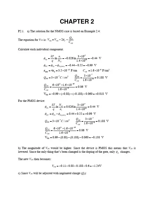
CHAPTER 2P2.1. a) The solution for the NMOS case is based on Example 2.4: The equation for V T0 is: 02BT FB F OXQ V V C φ=-- Calculate each individual component.1710()1362OX 077200611196310ln 0.026ln 0.44 V 1.4100.440.550.99 V 4 3.510 F/cm1.610 F/cm 310310/0.188 V 1.610610 1.6100.1.610i FpA GC Fp G gate OXB B OX OX OX n kT q NC Q Q C cmC Q C φφφφεε-------⨯==-=-⨯=-=--=-==⨯=⨯⨯=⨯==⨯⨯⨯⨯==⨯TO 06 V V 0.99(0.88)(0.188)0.0600.018 V=------=+ For the PMOS device:1710()77200611196TO 310ln 0.026ln 0.44 V 1.4100.440.550.99 V 310310/0.188 V1.610610 1.6100.06 V 1.610V 0.99(0.88)(0.188)0.0600.138 D Fn i GC Fn G gate B B OX OX OX N kT q n Q Q C cmC Q C φφφφ-----⨯===⨯=-=+=+⨯=⨯==⨯⨯⨯⨯==⨯=---=-Vb) The magnitude of V T0 would be higher. Since the device is PMOS this means that V T0 islowered. Since the only thing that’s been changed is the doping of the gate, only G φ changes. The new V T0 then becomes:00.110.880.1880.6 1.24V T V =----=-c) Since V T0 will be adjusted with implanted charge (Q I ):60.40.0180.382(1.610)(0.382)IOXIOXI Q C Q V C Q V -=-==⨯To calculate the threshold implant level N I :I I I I qN Q Q N q==For the NMOS device from part(a):6122190.610 3.8210/1.610I I Q N ions cm q --⨯=-=-=⨯⨯ (p-type) For the PMOS device from part(a):612219(1.610)(0.40.138)2.6210/1.610I I Q N ions cm q --⨯-=-=-=⨯⨯ (n-type) For the PMOS device from part(b):612219(1.610)(1.240.4)8.410/1.610I I Q N ions cm q --⨯-=-=-=⨯⨯ (p-type)d) The advantage of having the gate doping be n + for NMOS and p + for PMOS could be seen from analysis above. Doping the gates in such a way leads to devices with lower threshold voltages, but enables the implant adjustment with the same kind of impurities that used in the bulk (p-type for NMOS and n-type for PMOS). If we were to use the same kind of doping in gate as in the body (i.e. n + for PMOS and p + for NMOS) that would lead to higher un-implanted threshold voltages. Adjusting them to the required lower threshold voltage would necessitate implantation of the impurities of the opposite type near the oxide-Si interface. This is not desirable. Also, the doping of the poly gate can be carried out at the same time as the source and drain and therefore does not require an extra step.P2.2. First, convert ox t to units of cm:810100cm222210cm 10ox t -=⨯=ÅÅNow, using the mobility equation:()()20 1.8568130/V70cm0.8114102210pep nGS T ox cm V s V V t μμθ--==≈⎛⎫⎛⎫-+ ⎪⎪+ ⎪⎝⎭⎝⎭P2.3. a) For each transistor, derive the region of operation. In our case, for 0V,0.4V GS V =, thetransistor is in the cutoff region and there is no current. For 0.8V,1.2V GS V =, firstcalculate the saturation voltage Dsat V using:()GS T C DSAT GS T C V V E L V V V E L-=-+For our transistors, this would be:Next, we derive the IV characteristics using the linear and saturation current equations,we get the graphs shown below.IV Characteristic of NMOS01020304050607000.20.40.60.811.2Volts (V)C u r r e n t (u A )IV Characteristic of PMOSVolts (V)C u r r e n t (u A )To plot DS I vs. GS V , first identify the region of operation of the transistor. For GS T V V <, the transistor is in the cutoff region, and there is negligible current. For GS T V V > and GS DS V V ≤, the transistor is in the saturation region and saturation current expression should be used. The graphis shown below. Clearly, it is closer to the linear model.Ids vs. Vgs of NMOS010********607000.20.40.60.811.21.4Vgs (V)I d s (V )P2.4. For each transistor, first determine if the transistor is in cutoff by checking to see if V GS isless than or greater than V T . V T may have to be recalculated if the source of the transistor isn’t grounded. If V GS is less than V T , then it is in cutoff, otherwise, it is in either triode or saturation.To determine if it is in the triode saturation region, check to see if V DS is less than or greater than V DSAT . If V DS is less than V DSAT , then it is in triode, otherwise, it is in saturation. a. Cutoff00.200.2V0.4V GS G S T T GS TV V V V V V V =-=-===∴<b. Cutoff01.2 1.20V0.4V GS G S T T GS TV V V V V V V =-=-===∴<c. Linear01.20 1.2V0.4V GS G S T T GS TV V V V V V V =-=-===∴>The transistor is not in the cutoff region.()()()()()()1.20.460.20.48V 1.20.460.20.2V GS T C DSATGS T C DS DS DSATV V E L V V V E L V V V --===-+-+=∴<d. Saturation: In this case, because D G V V > the transistor is in the saturation region. To see this, recognize that in a long-channel transistor if D G V V >, the transistor is in saturation. Since the saturation drain voltage Dsat V is smaller in a velocity-saturated transistor than in a long-channel transistor, if the long-channel saturation region equation produces a saturated transistor, than the velocity-saturated saturation region equation will also.P2.5. In both cases, the first step it to calculate the maximum value of X V given G V . If thevoltage at the drain is higher than this maximum value, then ,max X X V V =, otherwise,X D V V =. The maximum value of X V is G T V V - but 0T T V V ≠ because of body effect andwe consider its effect.(),max 0001.20.40.988X G T G T G T G T V V V V V V V V V γγγγ=-=-+=--=--+=--=-There are two ways to calculate this, either through iteration or through substitution. Iteration:For the iteration method, we need a starting value for V X,max . A good starting value would be 0 1.20.40.8V G T V V -=-=. We plug this value on the RHS of the equation, calculate a new V X,max and repeat until we reach a satisfactory converged value.Old Vx,max New Vx,max 0.800 0.728 0.728 0.734 0.734 0.734In this, only three iterations are needed to reach 0.734V. Substitution:The term makes things a bit tricky, we get around this by making the following substitution:2,max 2,max 0.880.88X X x V V x =+∴=-Therefore:,max 220.9880.880.98800.2 1.87X V x x x =--=-=+-2,max 1.27, 1.470.880.733,1.28X x V x ===-=-= We use the first value since second value is above V DD . a. Since ,max D X V V >, ,max 0.733V X X V V ==. b. Since ,max D X V V <, ,max 0.6V X X V V ==. P2.6.a. Initially, when 0V in V =, the transistor is in the cutoff region and 0V X V =. Thisvalue is constant until V in exceeds V t 0. From then, X in T V V V =- and body effect must be taken into account. This trend continues until 0.7V X D V V ==, and the value of V inat that point must be calculated. From then on, 0.7V X D V V ==. To plot V X in the second region, we first derive an expression for V X vs. V in.(),max 0000.40.212X G T G T in T in T in in V V V V V V V V V V V γγγγ=-=-+=---=--=--=--Substituting:2,max2,max 0.880.88X X x V V x =+∴=-Therefore:,max 220.2120.880.21200.20.66X in in in V V x V x x V =---=--=+--220.880.88XxV x====-=-⎝⎭Since this is a quadratic function, there will be two graphs of V X. Only one of thesegraphs intersects with V X in the first region. In this case, plug 0.4inV= and see which one gives 0V. In our case, it would be the ‘+’ version of the quadratic.To see where region 3 begins, we simply isolate V in:()()()22220.880.2 2.710.2 2.71440.2 2.711.16V4XinVV=-⎝⎭-+-==+-==The final graph is shown in Figure 错误!未找到引用源。
数字集成电路设计方法、流程
数字集成电路设计方法、流程数字集成电路设计是指将数字电路功能进行逻辑设计、电路设计和物理布局设计,最终实现数字电路在集成电路芯片上的实现。
数字集成电路设计方法包括:1.设计需求分析:对于待设计的数字电路,首先需要了解设计需求。
明确电路所需的功能、性能指标、工作条件等,以确定电路设计的目标和约束条件。
2.逻辑设计:通过使用硬件描述语言(HDL)或者可视化设计工具,设计数字电路的功能逻辑。
在逻辑设计中,使用逻辑门、寄存器、计数器、状态机等基本逻辑单元,以及组合逻辑和时序逻辑的方法,实现所需功能。
3.电路设计:根据逻辑设计的结果,进行电路级设计。
包括选择和设计适当的电路模型、搭建电路拓扑、设计功耗、提高抗噪声性能等。
在电路设计中,需要考虑电源电压、电路延迟、功耗、抗干扰性能等因素。
4.物理布局设计:根据电路设计的结果,进行芯片级物理布局设计。
将电路中的逻辑单元和电路模块进行排布,设计电路的物理连接,并确定芯片的尺寸、引脚位置等。
物理布局设计需要考虑电路的功耗、面积、信号干扰等因素。
5.时序分析:对于复杂的数字电路,在设计过程中需要进行时序分析,以确保电路在各种工作条件下都能正常工作。
时序分析包括时钟分析、延迟分析、时序约束等。
6.仿真验证:在设计完成后,通过仿真验证电路的功能和性能。
使用仿真工具对电路进行功能仿真、逻辑仿真和时序仿真,验证设计的正确性。
7.物理设计:在完成电路设计和仿真验证后,进行物理设计,包括版图设计、布线、进行负载和信号完整性分析,以及完成设计规则检查。
8.集成电路硅掩模制作:根据物理设计结果,生成集成电路的掩模文件。
掩模文件是制造集成电路所需的制作工艺图。
9.集成电路制造:根据掩模文件进行集成电路的制造。
制造过程包括光刻、蚀刻、沉积、离子注入等工艺。
10.设计验证和测试:在集成电路制造完成后,进行设计验证和测试,确保电路的功能和性能符合设计要求。
数字集成电路设计的流程可以总结为需求分析、逻辑设计、电路设计、物理布局设计、时序分析、仿真验证、物理设计、硅掩模制作、集成电路制造、设计验证和测试等步骤。
数字集成电路设计实验报告
数字集成电路设计实验报告
摘要:
本实验旨在设计一个数字集成电路,实现特定功能。
本报告将介绍实验目的、背景和理论知识、设计方法、实验步骤、结果分析和讨论以及实验总结。
1.实验目的:
设计一个数字集成电路,实现特定功能,并通过实验验证设计的正确性和可行性。
2.背景和理论知识:
简要介绍数字集成电路的基本概念和原理,并介绍与本实验相关的理论知识,包括逻辑门、布尔代数、时序电路等。
3.设计方法:
本部分将详细介绍实验中采用的设计方法,包括采用的逻辑门类型、布尔代数的转换方法、时序电路的设计方法等。
4.实验步骤:
本部分将详细描述实验的具体步骤,包括电路图的绘制、器件的选择和布局、逻辑设计的步骤、时序电路的设计方法、电路的仿真等。
5.结果分析和讨论:
本部分将对实验结果进行分析和讨论,比较设计与实际结果的差异,分析可能的原因,并讨论实验的局限性和改进方向。
6.实验总结:
总结实验过程中的收获和经验,评估实验的结果和设计的可行性,并提出对未来工作的展望和建议。
通过对数字集成电路设计实验的详细介绍和分析,本报告旨在提供一份完整的实验报告,帮助读者理解实验过程和结果,并为今后的设计工作提供参考。
集成电路设计与实现技术分析
集成电路设计与实现技术分析随着计算机和信息技术的迅猛发展,集成电路设计与实现技术成为了现代电子工程研究领域的一大重点。
集成电路是一种将数十亿个晶体管、二极管、电容等元件集成在一起的现代电子器件,可以实现各种复杂的电路功能,并具有功耗低、速度快、尺寸小等优点。
本文将从集成电路设计的基本原理、设计流程、常用工具和实现技术等方面进行分析。
一、集成电路设计的基本原理集成电路设计的基本原理是将一个大的电路功能模块进行分解,然后将各个分解出的模块进行功能设计和物理细节设计,最后将各个模块组合在一起形成完整的电路。
具体来说,集成电路设计的基本原理包括以下五个方面:1. 电路设计原理。
在集成电路设计中,需要根据需要设计出各种电路模块,包括模拟电路、数字电路、混合电路等。
针对不同类型的电路,需要采取不同的设计方法和设计流程。
2. 设计目标和指标。
在集成电路设计时,需要根据实际需要确定设计目标和指标,包括性能、功耗、可靠性、成本等,以确保设计效果和实际应用效果相符合。
3. 物理细节设计。
在集成电路设计时,需要考虑到电子元器件的物理特性,包括电阻、电容、电感、晶体管等,并根据实际情况进行物理细节设计,包括原理图设计、布局设计等。
4. 制造和加工工艺。
在集成电路设计时,需要考虑到制造和加工工艺的要求,包括工艺流程、工艺控制、工艺变量等,以确保集成电路可以成功制造和完好运行。
5. 整个电路的优化设计。
在集成电路设计中,需要对整个电路进行优化设计,包括优化模型、线路优化、布局优化等,以确保电路的各项指标达到最优化的设计效果。
二、集成电路设计的流程分析集成电路设计的流程通常包括电路分解、电路设计分析、电路综合和验证等四个步骤。
具体流程如下:1. 电路分解。
将大的电路模块分解成若干个小模块,然后进行单独设计和测试。
2. 电路设计分析。
对单个模块进行电路设计,包括原理图设计、和布局设计等。
3. 电路综合。
将各个模块根据指定的规则进行组合,形成完整的电路。
电路中的数字集成电路设计与分析
电路中的数字集成电路设计与分析数字集成电路(Digital Integrated Circuit,简称DIC)是现代电子电路中的重要组成部分。
它们基于数字信号处理和逻辑运算,被广泛应用于计算机、通信、控制系统等领域。
本文将分析数字集成电路的设计原理和技术,并探讨其在电路中的应用。
一、数字集成电路的基本原理1.1 数字电路和模拟电路的区别数字电路是一种使用二进制数表示信息的电路,通过处理离散的数字信号进行逻辑运算;而模拟电路则是通过处理连续的模拟信号进行运算。
数字电路具有精确性高、噪声干扰小等优点,适合用于逻辑运算和信号处理。
1.2 数字集成电路的分类数字集成电路根据功能和结构可以分为多种类型,包括时序电路、组合电路和存储电路等。
其中时序电路用于时钟信号控制的功能电路,组合电路用于逻辑运算的功能电路,存储电路用于存储信息的功能电路。
二、数字集成电路的设计过程2.1 设计规划在进行数字集成电路设计之前,需要明确设计目标,包括功能需求、性能指标和设计约束等。
同时,还需对设计流程和设计工具进行规划,确保设计过程的有效性和可行性。
2.2 逻辑设计逻辑设计是数字集成电路设计的核心环节,通过逻辑门、触发器等基本模块的组合和连接,实现设计目标的功能和逻辑运算。
逻辑设计需要使用专业的设计语言和工具,如VHDL、Verilog等。
2.3 电路图设计电路图设计是将逻辑设计转化为具体的电路图的过程,包括将逻辑门、触发器等模块转化为相应的元件和连线。
在电路图设计中,需要考虑电路的布局和连接方式,以满足电路的性能指标和工艺要求。
2.4 仿真和验证仿真和验证是数字集成电路设计的重要环节,通过软件仿真和硬件验证,验证设计的正确性和稳定性。
仿真和验证过程需要使用仿真工具和测试设备,确保设计结果符合预期。
2.5 物理设计和布局物理设计和布局是将电路图设计转化为真实芯片的过程。
在物理设计中,需要考虑芯片的几何结构、层次布局和连线规划等。
[精品]数字集成电路分析与设计教学大纲.doc
数字集成电路分析与设计一、课程基本情况课程编号40260103开课单位微纳电子学系课程名称中文名称数字集成电路分析与设计英文名称Digital Integrated Circuit Analysis and Design教学目的与重点教学目的:1)让学生掌握数字集成电路的工作原理与分析方法2)让学生掌握数字集成电路与系统的设计流程和基本方法3)培养学生实际设计数字集成电路与系统的能力教学重点:1) CMOS反相器的特性,数字集成电路分析与设计的关键问题2)组合逻辑链的性能优化3)互连线的延时模型与分析4)同步时序电路的分析和设计5)数据通路运算单元的分析与设计6)存储器的工作原理的理解与分析课程负责人刘雷波吴行军课程类型□文化素质课□公共基础课□学科基础课□专业基础课■专业课□其它教学方式■讲授为主□实验/实践为主□专题讨论为主□案例教学为主□自学为主□其它授课语言■中文口中文+英文(英文授课>50%)□英文□其他外语学分学时学分 3 总学时48考核方式及成绩评定标准作业:15%,课程设计:15%,期中考试(闭卷):30%,期末考试(闭卷):40%教材及主要参考书中文外文教材数字集成电路一电路、系统与设计(第二版),JanM.Rabaey等著,周润德等译,电子工业出版社。
Jan M. Rabaey etc. “Digital Integrated Circuits , A Design Perspective (Second Edition)", Prentice Hall , 2003.主要参考书CMOS数字集成电路一分析与设计(第3版),Sung-Mo Kang等著,王志功等译,清华大学出版社(影Sung-Mo Kang, Yusuf Leblebici,"CMOS Digital IntegratedCircuits-Analysis and Design(ThirdEdition)".三、课程主要教学内容9.4高级互连技术9. 5综述9.6总结第10章存储器(6学时)(教材第12章)10.1分类10.2结构10.3内核--- 存储单元和阵列10.4外围电路10.5可靠性10.6总结。
数字集成电路分析与设计 第三章答案
CHAPTER 3P3.1. The general approach for the first two parameters is to figure out which variables shouldremain constant, so that when you have two currents, you can divide them, and every variable but the ones you want to calculate remain. In this case, since the long-channel transistor is in saturation for all values of V GS and V DS , only one equation needs to be considered:()()2112DS N OX GS T DS W I C V V V Lμλ=-+ For the last two parameters, now that you have enough values, you can just choose oneset of numbers to compute their final values.a. The threshold voltage, V T0, can be found by choosing two sets of numbers with the same V DS ’s but with different V GS ’s. In this case, the first two values in the table can be used.()()()()()()211122222201022001121121.2 1.210000.82800.8DS N OX GS T DS DS N OX GS T DS T DS T DS T T W I C V V V L W I C V V V LV I V I V V μλμλ=-+=-+-⎛⎫-===⎪--⎝⎭ 00.35V T V ∴=b. The channel modulation parameter, λ, can be found by choosing two sets of numberswith the same V GS ’s but with different V DS ’s. In this case, the second and third values in the table can be used.()()221 1.225010.8247DS DS I I λλ+==+ -10.04V λ∴=c. The electron mobility, µn , can now be calculated by looking at any of the first three sets of numbers, but first, let’s calculate C OX .631062-31m 10μm22?.210μm1m 10 0.0351 1.610/2.210OX OX t C F cm--=⨯⨯===⨯Now calculate the mobility by using the first set of numbers.()()()()()()()()()()()()22111021262101111 1.21 1.222210002cm 348V-s 1.610(4.75)1.20.3510.04 1.21DS N OX GS T DS N OX T DS N OX GS T DS W W I C V V V C V L LA I W C V V V L μλμλμμλ-=-+=-+===⨯-+-+d. The body effect coefficient gamma, γ, can be calculated by using the last set of numbers since it is the only one that has a V SB greater than 0V.()()()()244124414411221 1.20.468VDS N OX GS T DS DS GS T N OX DS GS T T GS W I C V V V LI V V W C V LV V V V μλμλ=-+-=+-==-==12000.6VT T T T V V V V γγγ=+-====P3.2. The key to this question is to identify the transistor’s region of operation so that gatecapacitance may be assigned appropriately, and the primary capacitor that will dischargedat a rate of V It C ∂∂= by the current source may be identified. Then, because the nodes arechanging, the next region of operation must be identified. This process continues until the transistor reaches steady state behavior. Region 1:Since 0V GS V = the transistor is in the cutoff region. The gate capacitance is allocated to GB C . Since no current will flow through the transistor, all current will come from the source capacitor and the drain node remains unchanged.68-151010V V 6.67100.6671510s nsSB V I I t C C -∆⨯====⨯=∆⨯ The source capacitor will discharge until 1.1V GS T V V == when the transistor enters thesaturation region. This would require that the source node would be at 3.3 1.1 2.2V S G GS V V V =-=-=.()15961510 3.3 2.2 1.6510s 1.65ns 1010C t V I ---⨯∆=∆=-=⨯=⨯ Region 2:The transistor turns on and is in saturation. The current is provided from the capacitor atthe drain node, while the source node remains fairly constant. The capacitance at the drain node is the same as the source node so the rate of change is given by:68-151010V V 6.67100.6671510s nsSB V I I t C C -∆⨯====⨯=∆⨯ Since the transistor is now in the saturation region, GS V can be computed based on thecurrent flowing through the device.()22 1.1 1.37V 3.3 1.37 1.93VGS T GST S G GS kW I V V LV V V V V =-==+==-=-=This is where the source node settles. This means that most of the current is discharged through the transistor until the drain voltage reaches a value that puts the transistor at the edge of saturation.3.3 1.1 2.2VDS GS TD G T V V V V V V =-=-=-=If we assume that all the current comes from the transistor, and the source node remains fixed, the drain node will then discharge at a rate equal to that of the source node in the first region. Region 3:The transistor is now in the linear region the gate capacitance is distributed equally to both GS C and GD C . and both capacitors will discharge at approximately the same rate.-151510V0.28621510510nsV I A t C μ-∆===∆⨯⨯+⨯The graph is shown below.00.511.522.533.5024681012Time (ns)V o l t a g e (V )P3.3. The gate and drain are connected together so that DS GS V V = which will cause thetransistor to remain in saturation. This is a dc measurement so capacitances are not required. Connect the bulk to ground and run SPICE. P3.4. Run SPICE. P3.5. Run SPICE. P3.6. Run SPICE. P3.7. Run SPICE.P3.8. First, let’s look at the various parameters and identify how they affect V T .∙ L – Shorter lengths result in a lower threshold voltage due to DIBL. ∙ W – Narrow width can increase the threshold voltage.∙ V SB – Larger source-bulk voltages (in magnitude) result in a higher threshold voltage. ∙ V DS –Larger drain-source voltages (in magnitude) result in a lower threshold voltage due to DIBL. The transistor with the lowest threshold voltage has the shortest channel, larger width, smallest source-bulk voltage and largest drain-source voltage. This would be the first transistor listed.The transistor with the highest threshold voltage has the longest channel, smallest width,largest source-bulk voltage and smallest drain-source voltage. This would be the last transistor listed. P3.9. Run SPICE.P3.10. Run SPICE. The mobility degradation at high temperatures reduces I on and the increasemobile carriers at high temperatures increase I off . P3.11. The issues that prompted the switch from Al to Cu are resistance and electromigration.Copper wires have lower resistances and are less susceptible to electromigration problems. Copper on the other hand, reacts with the oxygen in SiO 2 and requires cladding around the wires to prevent this reaction.For low-k dielectrics, the target value future technologies is 2.High-k dielectrics are being developed as the gate-insulator material of MOSFET’s. This is because the current insulator material, SiO 2, can not be scaled any longer due to tunneling effects.P3.12. Self-aligned poly gates are fabricated by depositing oxide and poly before the source anddrain regions are implanted. Self-aligned silicides (salicides) are deposited on top of the source and drain regions using the spacers on the sides of the poly gate. P3.13. To compute the length, simply use the wire resistance equation and solve for L .LR TWRTWL ρρ==First convert the units of ρ to terms of μm. Aluminum:2.7μΩρ=cm 6Ω10μΩ⨯610μm100cm ⨯()()()0.027Ωμm1000.812963μm 2.96mm0.027RTWL ρ=====Copper:1.7μΩρ=cm 6Ω10μΩ⨯610μm100cm ⨯()()()0.017Ωμm1000.814706μm 4.71mm0.017RTWL ρ=====P3.14. Generally, the capacitance equation in terms of permittivity constants and spacing is:k C WL tε=a. 4k = ()()()()230048.8510 3.541100SiO k k C WL TL t S S Sεε-====b. 2k = ()()()()30028.8510 1.771100k k C WL TL t S SSεε-====The plots are shown below.Capacitance vs. Spacing01234567800.511.522.533.544.555.5Spacing (um)C a p a c i t a n c e (f F)。
数字集成电路分析与设计 第七章答案
CHAPTER 7P7.1. Assume that all nodes start at 0V. The first row outputs will be at DD T V V -. Since thesenodes are also the gate nodes of the second row of transistors, their source nodes will be at 2DD T V V -. Likewise, the last row of transistors have voltages of 3DD T V V -. However, this value is below 0V so we leave them at 0V.1.2V1.2V0.73V 0.73V 0.73V0.33V0.33V0.33V0V0V0VP7.2. (a)(b)(c)(d)P7.3. (a) First calculate V Q .()01.80.51.15Q DD T DD T V V V V V Vγ=-=-+=--=Since this is slightly below 1.3V (voltage at which the PMOS turns on), we assume that the PMOS is slightly on. Since the PMOS’s V GS is quite low (because Q is high) and its V DS is quite high (because Q is low), the transistor is very likely in saturation. Similarly for the NMOS, because its V GS is high and its V DS is low, it’s likely in the linear region. Equating the two currents:()()()()()()()()22,,222211DSNDSN CN NQ Q CN NSDP sat DSN linV N N OX GSN T DSN P sat OX GSP T V GSP T CP PN V N N OX Q T Q P sat OX DD Q T V DD Q T CP PE L N I I W C V V V W v C V V V V E L L W C V V V W v C V V V V V V E L L μμ=---=-++----=--++For simplicity we shall assume that 11Q CN NV E L +≈ and220QV ≈.()()()2N N OX Q T QP sat OX DD Q T DD Q T CP P NW C V V V W v C V V V V V V E L L μ---≈--+Solve to produce:0.0080V Q V ≈When the CLK goes low, the intermediate output suffers from clock feedthough. To calculate the effects of clock feedthrough, let us first compute the capacitances involved. The capacitance from the clock signal to Q is:(.2/)(.2)0.0.4fF GS OL C C fF um um ===The capacitance from the Q to ground is:()()()(),310.2320.2 1.4fF Q DN IN inv d g C C C C W C W =+=+=+=The capacitive feedthrough equation is:()210.04 1.80.05V 0.04 1.41.150.05 1.1VGS CLK Q GS Q Q Q Q C V V C C V V V -∆∆===-++=+∆=-=To get the new value of Q V , first determine the determine the regions of operation of the transistors in the inverter by calculating V S . Then, once again, use the currentequations to determine Q V .Since the new voltage of V Q is still greater than the switching voltage, the transistors are in the same regions:()()()()()()2000460.4100.2810P N sat OX DD Q T Q N N OX Q T DD Q T CP P OXW L v C V V V V W C V V V V V E L C μ---≈---+⨯⨯≈()()()21.8 1.10.50.2270OX C --()()0.016V1.10.5 1.8 1.10.5 4.8≈---+(b) In this case 1.8Q DD V V V == and 0Q V =. Clock feedthrough has no effect since the transmission gate CLK signals cancel each other out.()()()()()()()(),3151515315(23)312.5102100.2110(2)0.23(210)(0.2)312.5101100.2257.532.5pass pass inv d inv eqn g eff g eqn d t R C R C R C W C W C W R C Wps ps ps----=+=+++⎡⎤=⨯⨯+⨯+⨯+⎣⎦⨯⨯=+=P7.4.a. Out A BC =+BBOutb. Out AB BC C =++Outc. ()Out A B C AB ABC AB =+++=+BBOutd. ()()1Out A B C AB ABC AB AB C AB A B =+++=+=+==+OutP7.5.a. ()Out A B C =+b. ()()Out A B C D E =+++ P7.6.a. Out A BC =+c bclkclkV DDb. Out AB BCC =++a bclkclkV DDc.()Out A B C AB ABC AB =+++=+V DDd.()()()Out A B C AB A B C A B AB=+++=+++=+aclkclkV DDP7.7.Assuming that one of the transistors in each transmission gate is being driven by a min-sized inverter:a.()()()()122333passinvRC R R RLERC R R+====b.()()()()()()()()313133313133AAinvCCinvRRC RLERC R RRRC RLERC R R========()()()()339333BBinvRRC RLERC R R====P7.8.a. Out A sel B sel =⋅+⋅b.R inv 6.25k ΩC inv,diff 1.2fF C pass,gate 0.8fF C pass,diff0.8fFR pass 6.25k ΩCpass,diff0.8fFCpass,gate0.8fFfC inv,gate2.4f fFCpass,diff0.8fFc. ()()(),,,,,,2A C inv inv diff pass gate pass diff inv pass inv gate pass gate pass diff t R C C C R R fC C C -=++++++ d. (),,inv inv LOADC out inv diff LOAD inv inv diffR R C t fC C R C f f-=+=+ e.()()()()(),,,,,,,,220inv inv diff pass gate pass diff inv pass inv gate pass gate pass diff inv LOADinv inv diff inv LOAD inv pass inv gate t R C C C R R fC C C R C R C fR C dtR R C df f f =++++++++=+-===3.2=P7.9. In both of these cases, the logical effort is the same due to the fact that the longest pathfrom output to ground is three transistors long. Assume that the CLK arrives ahead of the signals. Then,12()26663R R LE R λλ+== P7.10. We will use 0.18um technology and the node names below:W=4W=4OutFor the two inverter inputs:()()()3230.2 1.2fF inv g C C W ===For the pass gate inputs:()0.4fF pass g C C W ==At node x:()(3)(2) 1.4x eff eff g C C W C W C W fF =++=At node y:()2((2))(2)2y eff g eff C C W C W C W fF =++=At node Out:()((2))(2) 1.2out eff g eff C C W C W C W fF =++=The shortest path is through the one of the G ND input nodes to the output:()()()()min 212.5 1.4212.5 1.247.5x out t RC RC k fF k fF ps =+=+=The longest path is through one of the inverters to the output.()()()()()()max 2312.5 1.4212.52312.5 1.2112.5sx y out t RC RC RC k fF k fF k fF p =++=++=P7.11. At 0t =: DD F V =0X =?Y =.When the a goes high the first time, the voltage at X would be computed using the charge-sharing formula:()101.21V 210F DDX X F C V V C C ===++But because the maximum allowable voltage at node x is 0.734V, set 0.734V X V = Then recomputed V F :()()()()10 1.220.734 1.05V 10F DD X X F F C V C V V C --===When Phi goes down, F DD V V = and V X and V Y remains the same. The next time the Phi goes up, all the internal nodes are 0. When Phi goes down, F DD V V = and V X and V Y remains at 0. P7.12.P7.13.a. The input settings that give you the worst-case charge sharing are any of 1a c e === and both of 0b d ==. Essentially, what you are doing it trying to create the greatest amount of parasitic capacitances without creating a path to G ND .b. Assuming that transistors share nodes to reduce capacitance.()()()()()()()12*11125(3)(5) 5.2fF 333190.2 1.8fF 5.2 1.8 1.34V 5.2 1.8g d g d C C W C W C W C C W W W C V V C C =++==++=====++ The actual voltage would be larger than this since the internal node cannot rise above V DD -V T .c. This circuit fails if the worse case voltage falls below the switching voltage which can be computed to be V S =0.92V. Therefore, the circuit will operate properly. P7.14. Both of these circuits act as latches. When EN is on, there is a path from the output toeither V DD or G ND . The first latch is better than the second because the second latch suffers from charge sharing. When EN is off, there is no path from the output to either of the sources, if IN is switching it is possible for whatever charge that is held on OUT to be shared with the internal nodes between the two NMOS’s or the two PMOS’s. Therefore, the second one is not as good as the first one. P7.15.a.OUT OL X DD TV V V V V ==-b. First, let ’s find the required change in voltage:()()2OUT DD OLX DD T DD T TV V V V V V V V V ∆=-∆=+--=Now, let’s set up the clock feedthrough equation and solve for C b :22b OUT X b XX X T Xb OUT X DD OL TC V V C C V C V C C V V V V V ∆∆=+∆==∆-∆--。
vlsi数字集成电路一般设计流程
vlsi数字集成电路一般设计流程VLSI数字集成电路一般设计流程数字集成电路(VLSI)是现代电子技术领域的重要组成部分,广泛应用于计算机、通信、消费电子等领域。
VLSI数字集成电路的设计流程是一个系统性的过程,涉及到从需求分析到电路设计、验证、布局布线等多个环节。
本文将介绍VLSI数字集成电路的一般设计流程。
一、需求分析需求分析是VLSI数字集成电路设计的第一步,主要目的是明确设计要求和功能需求。
在需求分析阶段,设计团队与客户或项目经理进行沟通,了解项目的背景、功能要求、性能指标等。
同时,还需要考虑电路的功耗、面积、可靠性等因素,以确定设计的整体目标。
二、框架设计在框架设计阶段,设计团队根据需求分析的结果,确定整个电路的结构和功能模块。
框架设计需要考虑各个模块之间的连接方式、数据传输方式、时序要求等。
同时,还需要确定使用的逻辑门、存储器、寄存器等基本元件,并进行初步的电路图设计。
三、逻辑设计逻辑设计是VLSI数字集成电路设计的核心环节,主要目的是将框架设计的功能模块转化为逻辑电路。
在逻辑设计阶段,设计团队使用硬件描述语言(如Verilog、VHDL)进行电路的建模和描述,利用逻辑门、时序电路等元件进行电路的逻辑实现。
四、验证验证是确保电路设计正确性的重要环节。
在验证阶段,设计团队需要使用仿真工具对电路进行功能仿真,并设计测试用例进行验证。
通过仿真和测试,可以发现电路设计中的错误或潜在问题,并对其进行修复和优化。
五、布局布线布局布线是将逻辑电路转化为物理电路的过程。
在布局布线阶段,设计团队将逻辑电路转化为实际的布局图,确定各个元件的位置和相互之间的连线关系。
同时,还需要考虑电路的面积、功耗、信号延迟等因素,并进行布线优化。
六、物理验证物理验证是检验布局布线结果的环节。
在物理验证阶段,设计团队对布局布线后的电路进行电气规则检查(DRC)和电磁规则检查(ERC),以确保电路的物理完整性和可靠性。
根据验证结果,可以对布局布线进行调整和优化。
- 1、下载文档前请自行甄别文档内容的完整性,平台不提供额外的编辑、内容补充、找答案等附加服务。
- 2、"仅部分预览"的文档,不可在线预览部分如存在完整性等问题,可反馈申请退款(可完整预览的文档不适用该条件!)。
- 3、如文档侵犯您的权益,请联系客服反馈,我们会尽快为您处理(人工客服工作时间:9:00-18:30)。
问答:Point out design objects in the figure such as :design, cell, reference, port, pin, net, then write a command to set 5 to net ADesign: topReference: ADD DFFCell: U1 U2Port: A B clk sumPin: A B D QNet: A B SINSet_load 5 [get_nets A]why do we not choose to operate all our digital circuits at these low supply voltages? 答:1)不加区分地降低电源电压虽然对减少能耗能正面影响,但它绝对会使门的延时加大 2)一旦电源电压和本征电压(阈值电压)变得可比拟,DC特性对器件参数(如晶体管阈值)的变化就变得越来越敏感3)降低电源电压意味着减少信号摆幅。
虽然这通常可以帮助减少系统的内部噪声(如串扰引起的噪声),但它也使设计对并不减少的外部噪声源更加敏感)问道题:1.CMOS静态电路中,上拉网络为什么用PMOS,下拉网络为什么用NMOS管2.什么是亚阈值电流,当减少VT时,V GS =0时的亚阈值电流是增加还是减少?3.什么是速度饱和效应4.CMOS电压越低,功耗就越少?是不是数字电路电源电压越低越好,为什么?5.如何减少门的传输延迟? P2036.CMOS电路中有哪些类型的功耗?7.什么是衬垫偏置效应。
8.gate-to-channel capacitance C GC,包括哪些部分VirSim有哪几类窗口3-6. Given the data in Table 0.1 for a short channel NMOS transistor withV DSAT = 0.6 V and k′=100 µA/V2, calculate V T0, γ, λ, 2|φf|, and W / L:解答:对于短沟道器件:2'min min [()](1)2DGS T DS V WI k V V V V L λ=--+ min min[(),,]GS T DS DSAT V V V V V =-在选择公式的时候,首先要确定工作区域,表格中的所有V DS 均大于V DSAT ,所以不可能工作在线性区域。
如果工作在饱和区域则: V T 应该满足 : V GS -V T <V DSAT 2-V T <0.6 1.4<V T这是不可能的,所以可以假设所有的数据都是工作在速度饱和区域 所以:2'[()](1)2DSAT D GS t DSAT DS V WI k V V V V L λ=--+由 1&22'00.6[(2.5)0.6](1 1.8)18122D W I k Vt L λ=--+=2'00.6[(2)0.6](1 1.8)12972D W I k Vt L λ=--+= 20200.6(2.5)0.61812212970.6(2)0.62Vt Vt --=--0.44VtV=(01.4Vt V<) 所以 1,2,3是在速度饱和区由 2&312971 1.813611 2.5λλ+=+10.08V λ-=由 2&4 1297/1146=[(2-Vt0)x0.6-o.62/2]/[(2-Vt)x0.6-0.62/2] Vt=0.587V由 2 &5 Vt=0.691V这两个值都满足 Vt<1.4, 所以表中的数据都是工作的速度饱和状态0(22)SB f fVt Vt V γφφ=++-由4 &5 和 00.44Vt V=可以计算出20.6f Vφ= 和1/20.3V γ=2'1297[()]2DSAT DGS t DSAT V WI A k V V V L μ==-- 得到 W/L=1.53-7 Giv en Table 0.2 ,the goal is to derive the important device parametersfromthese data points. As the measured transistor is processed in a deep-submciron technology, the‘unified model ’ holds. From the material constants, we also could determine that the saturation voltage V DSAT equals -1V. You may also assume that -2ΦF = -0.6V.NOTE: The parameter values on Table 3.3 do NOT hold for this problem. a. Is the measured transistor a PMOS or an NMOS device? Explain your answer.b. Determine the value of VT0.c. Determine γ.d. Determine λ.e. Given the obtained answers, determine for each of the measurements the operation region of the transistor (choose from cutoff, resistive, saturated, and velocity saturated ). Annotateyour finding in the right-most column of the above.解答:a) 这是 PMOS 器件 b) 2'min min[()](1)2D GS T DS V WI kV V V V Lλ=--+比较各表中(),,GS T DS DSAT V V V V -的值知道1,4为工作在速度饱和状态由 1&42'[()](1)2DSAT D GS t DSAT DS V WI k V V V V L λ=--+2'01[( 2.5)(1)](1*( 2.5))84.3752D W I k Vt L λ=----+-=-2'01[( 2.0)(1)](1*( 2.5))56.252D W I k Vt L λ=----+-=-20201( 2.5)(1)84.375256.251( 2.0)(1)2Vt Vt -----=-----Vt 0=0.5Vc) 由 1&5和上面求出的Vt0的值: 1,5工作在速度饱和区域 则:(-84.375)/(-72.0)=[(-2.5-Vt0)*(-1)-12/2]/[(-2.5-Vt)*(-1)-12/2]求出Vt ,代入下面公式:0Vt Vt γ=+-求出:γ=0.538V 1/2d)由 1&6,因为1,6均工作在速度饱和区域:84.3751( 2.5)80.6251( 1.5)λλ-+-=-+-λ=0.05V -1e)1-vel. Sat, 2-cutoff, 3-saturation , 4-5-6 vel. Sat, 7-linear3-8 An NMOS device is plugged into the test configuration shown below in Figure0.4. The input V in =2V. The current source draws a constant current of 50 µA. R is a variableresistor that can assume values between 10k Ω and 30 k Ω. Transistor M1 experiences short channel effects and has following transistor parameters: k ’ = 110*10-6 V/A2, V T = 0.4 ,and V DSAT = 0.6V. The transistor has a W/L = 2.5µ/0.25µ. For simplicity body effect andchannel length modulation can be neglected. i.e λ=0, γ=0. .a. When R =10k Ω find the operation region, V D and V S .b. When R= 30k Ω again determine the operation region V D , V Sc. For the case of R = 10k Ω, would V S increase or decrease if λ ≠ 0. Explain qualitatively解答:1)当 R=10k, V D =V DD -IRV D =2.5-50x10-6x104=2.5-0.5=2V假设器件工作在饱和区 ( 需要以后验证)则:2'()50D GS t WI K V V A Lμ=-= GS t V V -=0.3V 所以 V GS =0.3+0.4=0.7VV S =2-0.7=1.3VVmin=min(V GS -Vt, V DSAT , V DS )=min(0.3,0.6,0.7)=V GS -Vt 所以是饱和区V D =2VV S =1.3V saturation operationb) V D =2.5-30x103x50x10-6=2.5-1.5=1V assume linear op:2'()]502DS DGS t DS V WI K V V V A L μ=--=26(1)1101010(20.4)(1)]502S S S V V V Aμ--⨯⨯----= 0.93S V V=Min(V GS -V T ,V DS ,V DSAT )=min((1-0.93-0.4).0.07,0)=V DS SO linearc) increas e , R = 10k Ω2'()(1)D GS t DS WI K V V V Lλ=-+ R 变化,则V D 必须变化以保持电流稳定,(1)DS V λ+试图增加电流,而为了恒定电流值,V GS 必须减小,即V S 必须增加 1、(10)P137Assume an inverter in the generic 0.25 mm CMOS technology designed with a PMOS/NMOS ratio of 3.4 and with the NMOS transistor minimum size (W = 0.375 mm, L = 0.25 mm, W /L =1.5). V M = 1.25 V, please compute V IL , V IH , N ML , N MH . the processparametersispresentedintable1()(/2)(1)DM n DSATnin Tn DSATn n out IV k VV V V V λ=--+由此可以得到 V IL , V IH , NM L , NM H :因为V IH =V M -V M /g , V IL =V M +(V DD -V M )/g NM H =V DD -V IH , NM L =V IL V IL =1.2V, V IH =1.3V, NM L =NM H =1.25.3、For the inverter of Figure 1 and an output load of 3 pF ,at Vout=2.5V, I DVsat =0.439mA, at Vout=1.25V, I D vsat=0.41mAfig 1a. Calculate t plh , t phl , and t p .b. Are the rising and falling delays equal? Why or why not? 解答:t pLH =0.69R L C L = 155 nsec.对于 tp HL :首先计算 R on for V out at 2.5V and 1.25V. 因为 Vout=2.5V, I DVsat =0.439mA 所以 Ron= 5695 当 Vout=1.25V, IDvsat=0.41m 所以Ron= 3049.这样, Vout=2.5Vand Vout=1.25V 之间的平均电阻 Raverage=4.372k t pLH =0.69RaverageC L =9.05nsec. t p =av{t pLH , t pHL }=82.0nsecb. Are the rising and falling delays equal? Why or why not? Solutiont pLH >> t pHL 因为 R L =75k 远大于有效线性电阻 effective linearized on-resistance of M1.5-5 The next figure shows two implementations of MOS inverters. The first inverter uses onlyNMOS transistors. Calculate V OH , V OL , V M for each case. 有的参数参考表1解答:电路 A.V OH: 当 M1关掉, M2 的阈值是:当下面条件满足的时候,M2将关闭:所以 V OUT=V OH=1.765VV OL: 假设V IN=V DD=2.5V.我们期望 V OUT为低, 因此我们可以假设M2工作在速度饱和区,而M1工作在线性区域.因为 I D1= I D2 , 所以 V OUT=V OL=0.263V, 假设成立V M: 当V M=V IN=V OUT.假设两晶体管均工作在速度饱和区域, 我们得到下面两个方程:设 I D1=I D2, 得到 V M=1.269V电路 B.当 V IN=0V, NMOS 关掉,PMOS 打开,并把V OUT拉到VDD, so V OH=2.5. 同样, 当 V IN=2.5V, the PMOS关掉,NMOS 把 V OUT拉到地, 所以V OL=0V.为了计算 V M: V M=V IN=V OUT.假设两晶体管均工作在速度饱和区域,可以得到下面两组方程.设 I D3+ I D2 =0 ,可以得到r V M = 1.095V.所以假设两晶体管均工作在速度饱和区域是正确的.5-7Consider the circuit in Figure 5.5. Device M1 is a standard NMOS device. Device M2 has allthe same properties as M1, except that its device threshold voltage is negative and。