PCB常见不良中英文对照电子厂专业术语
中英对照PCB专业术语精选全文

analog circuit
模拟电路
amplitude
电压幅度
amp-hour
安培小时
amperometric titration
电流滴定
ampere
安{培)
amorphous thin film
非晶薄膜
amorphous thin film
非晶薄膜
amorphous semiconductor material
单向导电膜安装,各向异性导电膜连接
anisotropic conductive contact
单向导电接触,各向异性导电接触
anisotropic conductive adhesives
单向导电黏结剂,各向异性导电黏结剂
angstrom unit
埃单位
angle rotor
角转头
angle of contact
烷基咪唑
alkaline permanganate solution
碱性高锰酸盐溶液
alkaline etchant
碱性蚀刻液
alkaline degreasing
化学除油
alkaline cleaner
破性清洗液
alkaline ammonia etchant
氨碱蚀刻液
ALIVH
任意层内导通孔
aliphatic solvent
adhesion promotion
增教处理,附着力增强
by-product
副产品,副产物
butt lead
搭接引线,对接引线
butting connector
对接引脚
butter coat
厚涂层,外表树脂层
不良中英文对照表
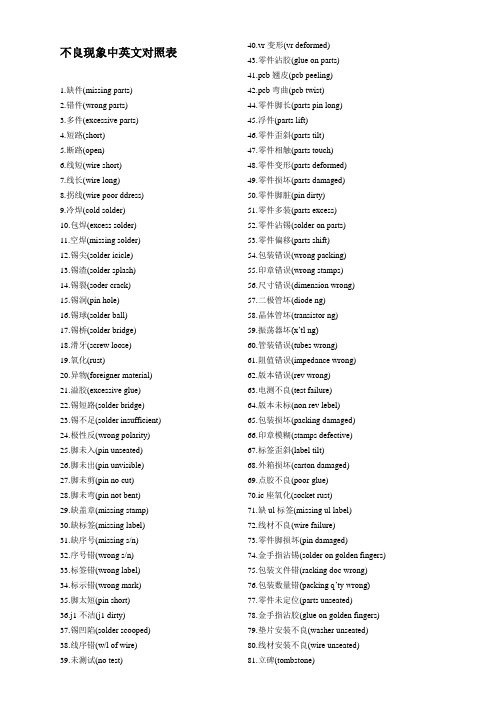
不良现象中英文对照表1.缺件(missing parts)2.错件(wrong parts)3.多件(excessive parts)4.短路(short)5.断路(open)6.线短(wire short)7.线长(wire long)8.拐线(wire poor ddress)9.冷焊(cold solder)10.包焊(excess solder)11.空焊(missing solder)12.锡尖(solder icicle)13.锡渣(solder splash)14.锡裂(soder crack)15.锡洞(pin hole)16.锡球(solder ball)17.锡桥(solder bridge)18.滑牙(screw loose)19.氧化(rust)20.异物(foreigner material)21.溢胶(excessive glue)22.锡短路(solder bridge)23.锡不足(solder insufficient)24.极性反(wrong polarity)25.脚未入(pin unseated)26.脚未出(pin unvisible)27.脚未剪(pin no cut)28.脚未弯(pin not bent)29.缺盖章(missing stamp)30.缺标签(missing label)31.缺序号(missing s/n)32.序号错(wrong s/n)33.标签错(wrong label)34.标示错(wrong mark)35.脚太短(pin short)36.j1不洁(j1 dirty)37.锡凹陷(solder scooped)38.线序错(w/l of wire)39.未测试(no test) 40.vr变形(vr deformed)43.零件沾胶(glue on parts)41.pcb翘皮(pcb peeling)42.pcb弯曲(pcb twist)44.零件脚长(parts pin long)45.浮件(parts lift)46.零件歪斜(parts tilt)47.零件相触(parts touch)48.零件变形(parts deformed)49.零件损坏(parts damaged)50.零件脚脏(pin dirty)51.零件多装(parts excess)52.零件沾锡(solder on parts)53.零件偏移(parts shift)54.包装错误(wrong packing)55.印章错误(wrong stamps)56.尺寸错误(dimension wrong)57.二极管坏(diode ng)58.晶体管坏(transistor ng)59.振荡器坏(x’tl ng)60.管装错误(tubes wrong)61.阻值错误(impedance wrong)62.版本错误(rev wrong)63.电测不良(test failure)64.版本未标(non rev lebel)65.包装损坏(packing damaged)66.印章模糊(stamps defective)67.标签歪斜(label tilt)68.外箱损坏(carton damaged)69.点胶不良(poor glue)70.ic座氧化(socket rust)71.缺ul标签(missing ul label)72.线材不良(wire failure)73.零件脚损坏(pin damaged)74.金手指沾锡(solder on golden fingers)75.包装文件错(racking doc wrong)76.包装数量错(packing q’ty wrong)77.零件未定位(parts unseated)78.金手指沾胶(glue on golden fingers)79.垫片安装不良(washer unseated)80.线材安装不良(wire unseated)81.立碑(tombstone)。
PCB及PCBA缺陷中英文对照表

PCB及PCBA缺陷中英文对照表PCB及PCBA缺陷中英文对照表1板面凹痕dent 41漏印字符skip2内层白斑I/L white spot 42金粗Au too big3线路缺口circuit nick 43金簿Au too thin4蚀刻不净undering etching 44金手指缺口G/F voids/nick on G/F 5绿油剥离S/M peel off 45金手指发黑G/F too black6显影不净under developing 46字符印反inverse C/M7基材白点laminate measling 47金手指针孔G/F pinholes8铜面氧化copper oxide 48标志不清symbol unclear9绿油上焊盘s/m on pad 49标志错symbol wrong10白字上焊盘c/m on pad 50绿油鬼影ghost in S/M11阻焊不良poor S/M 51手指印finger print12线路擦花track scratch 52补线不良poor line repairing13锡上线sn on circuit 53锡高exessive solder14聚锡sn mass 54孔小hole undersize15锡灰sn gray 55字符错wrong C/M16焊盘露铜cu exposed on pad 56字符印偏C/M misalignment17锡上金手指sn on G/F 57字符入孔C/M in hole18金手指凹痕G/F dent 58字符重影C/M doubloe image19金手指擦花G/F scratch 59漏镀金手指missing plating G/F20金手指粗糙G/F roughness 60金手指发白G/F gray21v-cut不良poor V-cut 61焊盘脱落pad break off/pad peel off 22倒边不良poor milling 62焊盘露铜pad expose cu23针床压伤ET dent 63断绿油桥missing S/M bridge24拖锡不良poor touch up 64塞孔block hole25补金不良poor repairing Au 65水迹water print26补油不良poor repairing s/m 66锡珠solder ball27针孔pinhole 67砂孔pitting28胶渍paster stain 68油薄S/M too thin29k孔内毛刺burrs in hole 69聚油excess solder mask 30锡珠入孔solder in hole 70锡粗Sn too thick31露铜expose Cu 71线路上锡Sn overlap scratch 32露镍expose Ni 72绿油下杂物contamination under S/M 33绿油起泡solder mask blister 73焊盘损坏land damage34绿油起皱solder mask winbles 74焊盘翘起lifted land35金手指氧化G/F oxiding 75偏位misregistration36金颜色不良Au discoloration 76漏钻孔missing hole37金面凸起Au surface blister 77焊盘缺口nick on pad 38绿油入孔solder mask in hole 78线路缺口nick on track 39爆板board angle damafe40翘板warp1开路open circuit 46焊盘翘起lifted land2短路short circuit 47漏钻孔missing hole线路狗牙circuit wist 48露布纹weave exposure3线路缺口circuit nick 49钻偏孔hole misregistratiion 4线路凹痕circuit dent 50孔损害hole damage5渗镀plating Bloody 51基材分层delamination6焊盘缺口pad nick 52蚀刻过度over etching7内层白斑I/L white spot 53多孔hole too much8黑化不良poor B.O 54残铜remain Cu9爆板measling 55孔内露基材laminate exposure in hole10粉红圈pinking ring 56焊盘脱落pad break off 11层压起泡press blister 57焊盘凹痕pad dent12错位misregistation 58焊盘凸起pad bulge13偏位shift 59焊盘损坏pad damaged14孔内无铜no Cu on Pth 60焊盘缺口pad nick15孔内毛刺hole burrs 61焊盘露铜pad expose Cu 16NPTH有铜Cu on NPTH 30修理不良poor repairing17铜面露基材exposed laminate 31铜薄copper too thin18铜面凹痕dent on Cu surface 32内层擦花I/L scratch19胶渍gum residue 33内层偏位I/L misregistation20夹膜D/F nip 34内层杂物I/L inclusions21蚀刻不尽under etching 35掉膜film off22线幼line too thin 36干膜碎D/F meaking23孔大hole oversize 37退锡不尽poor Sn stripping 24孔小hole undersize 38间隙小space too marrow 25偏孔hole misregistration 39板薄board too thin26铜面瘤粒Cu nodule 40板厚board too thickness27显影不尽under developing 41针孔pinhole28铜面刮伤scratch on Cu surface 42崩孔breakout29塞孔hole plugged 43侧蚀undrcut45亚色dull colour 44镀层粗糙plating layer roughness PCB及PCBA常用度量衡单位换算所属目录:FASTPCBA靖邦公司资料发布时间:2009-01-01 1英尺=12英寸1英寸inch=1000密尔mil1mil=25.4um1mil=1000uin mil密耳有时也成英丝1um=40uin(有些公司称微英寸为麦,其实是微英寸)1OZ=28.35克/平方英尺=35微米H=18微米4mil/4mil=0.1mm/0.1mm线宽线距1ASD=1安培/平方分米=10.76安培/平方英尺1AM=1安培分钟=60库仑主要用于贵金属电镀如镀金1平方分米=10.76平方英尺1盎司=28.35克,此为英制单位1加仑(英制)=4.5升1加仑美制=3.785升1KHA=1000安小时1安培小时=3600库仑比重波美度=145-145/比重SG.SG.比重(克/立方厘米)=145/(145-波美PCB及PCBA行业专用名词PCB及PCBA行业专用名词BOM(Bill of material) 物料需求單Laminate 基板Copper foil 銅箔Solder mask(s/m) 防焊Bare Board 空板Microetching 微蝕Exposure 曝光Dry Film 干膜Matte side 毛面Rcc(Resin coated copper) 背膠銅箔Final shaping 成型Electrical test(ET) 電測Visual Inspection 外觀檢查Gold Finger(G/F) 金手指Legend 文字Post Cure 后烤Desmear 除膠渣Developing 顯影Pattern Plating 線路電鍍Panel Plating 全板電鍍Puddle Effect 水坑效應Oxide Coating 黑氧化Routing Bit 銑刀Tolerance 公差Post Treatment 后處理Adhesion 附著力Stripping 去膜Baking 烘烤AQL(acceptable quality level) 品質允收水準Optical Target 光學靶點Lay up 疊合Chromation 鉻化處理Undercut 側蝕Microvia 微孔Annular Ring 孔環Burr 毛頭Entek 有機保焊處理Conformal Mask 銅窗Drum Side 光面Diazo Film 偶氮棕片Cut Lamination 下料Sheets Cutting 裁板Inner Layer Drilling 內層鑽孔Outter Layer Drilling 一次孔2nd Drilling 二次孔PCB及PCBA专用名词Laser Drilling 雷射鉆孔Blind&Burried Hole Drilling 盲(埋)孔鉆孔screen printing 網版印刷silk screen 絲網印刷scum 透明殘膜skip printing 跳印漏印squeege 刮刀type 种類abietic acid 松脂酸air knife 風刀bridging 搭橋橋接flux 助焊劑product process 制程pre-process 制前solder bridge 錫橋soler bump 錫突solder plug 錫塞immersion gold 浸金(化金)thin core 薄基板twist 板翘, 板扭warp ,warpage 板彎weave eposure 織紋顯露wicking 燈蕊效應yield 良品abrasion resistance 耐磨性absorption 吸收accelerated test 加速實驗acceleration 速化反應accelerator 加速剂batch 批cold solder joint 冷焊點component side 零件面double side 雙面double side board 雙面板fiducial mark 基準記號finished board 成品板lot size 批量rack 掛架register mark 對準用標記solder side 錫鉛面thickness 厚度warehouse 仓库wet process 濕制程Beveling 斜邊chamfer 道角dimension 尺寸Fixture 治具interconnection 互相連通line space 線距line width 線寬misregistration 對不准mouse bite 蝕刻缺口nick 缺口master drawing 主圖print and etch board 印刷後及蝕刻後板crease 皺褶dent 凹陷glass fiber 玻璃纖維布pin hole 針孔pit 凹點target hole 靶孔PCBA及PCB专用名词(二)PCBA及PCB专用名词(二)Black Oxide Removal 黑化還原Plug Hole 塞孔Ink Print&precure 印刷及預烤Scrub 表面處理Spray Coating 靜電噴涂Printing of Legend 文字印刷Pumice ( Wet Blasting) 噴砂Immersion Ni/Au(Electoless Ni/Au) 浸鎳金Hot Air Solder Leveling 噴錫N/C routing 撈型Beveling of G/F 金手指斜边Cleanning&Baking 清洗及烘烤Fixture Testing 治具測試original A/W 客戶原稿working A/W 工作片working master 工作母片carlson pin 定位梢component hole(>30mil) 零件孔drill facet 鑽尖切削面drill pointer 鑽尖重磨機drilled blank board 已鑽孔的裸板hole diameter 孔徑hole location 孔位hole number 孔數lay back 刃角磨損margin 鑽頭刃帶open circuits 斷路runout 偏轉slot 開槽spindle 鑽軸tooling hole 工具孔stacking structure 疊板結構blow hole, void in PTH hole 吹孔孔破deburring 去毛頭electroless-deposition 無電鍍化etchback 回蝕air inclusion 氣泡chase 網框fabric 網布liquid 液態\狀mealing 泡點trim line 裁切線v-cut v型切槽golden board 標準板back lighting 背光crack 裂痕crazing 白斑dimension stability 尺寸安全性failure 故障fault 缺陷瑕疵gap 鑽尖分開gel time 膠化時間haloing 白邊白圈hardener 硬化劑hole counter 數孔機hook 外弧insulation resistance 絕緣阻抗ionizable(ionic) contaminants 離子性污染land 焊墊microsectioning 微切片法negative etchback 反回蝕overlap 鑽尖重曡peel strength 抗撕強度pink ring 粉紅圈REJ(reject) 拒收退貨release agent(sheets) 脫膜劑resin content 膠含量resin flow 膠流量resin recession 樹脂下限resin smear 膠渣rework 重工specification(spec.) 規範innerlayer&outlayer 內外層gold plating 鍍金QC(quality control) 品管back up 墊板blister 起泡局部分层caul plate 隔板, 钢板open circuits 断路sampling size 抽樣數edge spacing 板邊空地ground plane 接地層laminator 壓膜機M/T 磁帶disk 磁片。
PCB专业用语中英文对照

PCB专业用语中英文对照PCB,全称是Printed Circuit Board,即印制电路板,是电子器件中不可缺少的一部分。
在PCB的生产和使用过程中,有许多特定的专业术语,以下将列出一些常见的PCB专业用语的中英文对照,以帮助PCB行业的从业人员更好地了解和使用这些术语。
1. Pad - 表面贴装元件引脚焊盘2. Via - 通孔3. Trace - 线路走线4. Solder mask - 焊盘阻焊5. Silkscreen - 字体绘制6. Substrate - 基板7. RoHS - 过度有害物质限制指令8. PCB Assembly - PCB组装9. Panel - 夹板10. Gerber file - Gerber文件(PCB板图文件的一种)11. Copper weight - 铜箔厚度12. SMD - 表面贴装元件13. Through-hole - 贯通孔除此之外,还有一些专业用语需要注意:1. Blind via - 盲孔2. Buried via - 埋孔3. Soldering - 焊接4. Copper pour - 铜泡5. Annular ring - 环形垫片6. Plated through-hole - 化学镀铜孔7. Gold finger - 金手指(PCB板边部的带触点金属部件)8. OSP - 有机锡防护(一种PCB表面处理方法)以上仅列举了部分PCB专业用语的中英文对照,如需更全面的了解,需要从事相关行业或有专业经验的人士掌握更多知识。
在PCB制造和使用过程中,正确使用这些专业用语是非常重要的,它们不仅可以帮助我们更好地了解PCB的生产过程和使用方法,还可以提高工作效率和避免出现误解和错误。
不良描述中英文对照
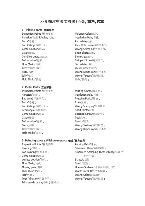
不良描述中英文对照(五金,塑料,PCB) 1.Plastic parts 塑膠部件-Inspection Points /檢查要點: Abrasion/划痕,Bubbles/气泡, Burrs/毛刺,Bad Plating/電鍍不良, Contamination/雜質,Crack/爆裂,Combine Lines/結合線, Deformation/變形,Flow Marks/流痕,Greasy Dirt/油污,Haze/霧狀,Jelly/泠膠,Mold Marks/模痕, Melange Color/混色, Oppilation Hole/盲孔,Pull White/拉白,Pour Hole uneven/澆口不平, Wrong Stamping/字麥不符, Short Shots/缺料, Shrinkage/縮水,Stripped Screw/螺絲滑牙, Top White/頂白,Weld Lines/夾水紋,Wrong Dimension/尺寸不符, Wrong Texture/紋理錯誤, Light/發亮;-质量-2. Metal Parts 五金部件Inspection Points /檢查要點: Abrasion/划痕,Bad Weld/焊接不良,Burrs/毛刺,Bad Plating/電鍍不良, Bend angle/折彎角度, Contamination/雜質, Crack/爆裂,Deformation/變形,Dents/凹痕,Greasy Dirt/油污,Mold Marks/模痕, Missing Stamp/漏沖壓, Oppilation Hole/盲孔, Pressing Marks/壓痕,Rust/生鏽,Wrong Stamping/字麥錯誤, Short Shots/缺料,Stripped Screw/螺絲滑牙,Pits/疤痕,Specks/斑點Wrong Texture/紋理錯誤, Wrong Dimension/尺寸不符;bb3. Painting parts / SilkScreen parts 噴油/絲印部件Inspection Points /檢查要點: Bleeding/滲色,Bad Painting/噴油不良, Contamination/雜質,deviate position/偏位,Flow Marks/流痕,Missing paint/漏噴,Over Paint/肥油,Pits/疤痕,Poor Adhesion/附著力差,Print Words Leans/印刷字體傾斜, Pooring Paint/薄油,Silkscreen Haze/絲印模糊,Silkscreen Stamping Inconsistency/絲印字樣不一致,Scratch/划傷,Speck/斑點,Uneven Surface Oil/表面油層不均勻, Words Break Off/字体斷開,Wrong Color/錯誤顏色,Wrong Texture/紋理錯誤;-4. PCB 印制线路板Open/开路;Short/短路;Weave Texture/板料席纹; Foreign Residue/外来杂物; Delamination/爆板,分层;Dent/凹陷;Dent on G/F/金手指凹陷; Scratch/擦花;Misregistration/对位不正;Board Damage/板子损坏;C/M Illegible/白字不清;C/M on pad/白字上垫;Copper expoure/露铜;Solder Mask on Pad/绿油上垫; Uneven Solder Mask/绿油不平均; Solder Mask peeling off/绿油脱落; Missing Hole/漏孔; Excess Hole/多孔;Wrong Hole Size/孔径错误;Hole Breakout/崩孔;Nick Trace/线路缺口;Void on Trace/线路铜穿;Diskdown/线路不良/狗牙;Solder Mask inside hole/绿油入孔; Discolouration under Solder Mask/绿油颜色不良;Foreign matter under Solder Mask/绿油下杂物;Solder Mask skipping/不过油;Solder on Gold Finger/金手指上锡;Poor Bevelling/斜边不良;Gold Finger burrs/金手指损坏;Ping Ring/粉红圈.5. Electronic parts 电子元件No AVL/没AVL;not on AVL/不在AVL上;Mfg/Mfg P/N dis-match AVL/ 与AVL不符; D/C overdue/ D/C 过期;无D/C;wrong part/错料;no reel/无卷轴;bulk packing for chip/ 散装;No dry packing(HIC change color)/ 无真空包装(防潮卡变色);No ESD packing/无防静电包装;illegible marking/印字不清,wrong marking/印字错;deformation/变型;micro crack/裂料;damaged part/ 烂料;Lead bent(PTH/SMT)/脚弯;Solder balls damaged/锡球坏wrong lead form/脚型错;wrong pitch/脚距不符;coplanar problem/平整度不良; pad(lead) oxidization/锡垫(引脚)氧化; wrong direction in tape(tray)/带中(盘中)方向错;short pins/引脚短;failed in solderability/ 焊锡不良;size(dimensions) out of specification/ 尺寸超标;function fail/ 功能不良;no tolerance/无误差范围; contamination/杂质;wrong identification for pin1/ 第1脚标识错.Broker Buy/炒料;(巻装物料)巻带前无空余巻带No blank cover tape for feeder loading巻带粘力不足Not enough adhesive for the cover tape. 料盤变形Reel Deforming/卷带变型.。
PCB及PCBA缺陷中英文对照表
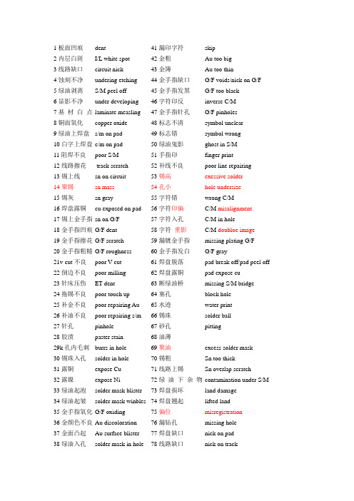
1板面凹痕dent 41漏印字符skip2内层白斑I/L white spot 42金粗Au too big3线路缺口circuit nick 43金簿Au too thin4蚀刻不净undering etching 44金手指缺口G/F voids/nick on G/F5绿油剥离S/M peel off 45金手指发黑G/F too black6显影不净under developing 46字符印反inverse C/M7基材白点 laminate measling 47金手指针孔G/F pinholes8铜面氧化copper oxide 48标志不清symbol unclear9绿油上焊盘s/m on pad 49标志错symbol wrong10白字上焊盘c/m on pad 50绿油鬼影ghost in S/M11阻焊不良poor S/M 51手指印finger print12线路擦花 track scratch 52补线不良poor line repairing13锡上线sn on circuit 53锡高exessive solder14聚锡sn mass 54孔小hole undersize15锡灰sn gray 55字符错wrong C/M16焊盘露铜cu exposed on pad 56字符印偏C/M misalignment17锡上金手指sn on G/F 57字符入孔C/M in hole18金手指凹痕G/F dent 58字符重影C/M doubloe image19金手指擦花G/F scratch 59漏镀金手指missing plating G/F20金手指粗糙G/F roughness 60金手指发白G/F gray21v-cut不良poor V-cut 61焊盘脱落pad break off/pad peel off 22倒边不良poor milling 62焊盘露铜pad expose cu23针床压伤ET dent 63断绿油桥missing S/M bridge24拖锡不良poor touch up 64塞孔block hole25补金不良poor repairing Au 65水迹water print26补油不良poor repairing s/m 66锡珠solder ball27针孔pinhole 67砂孔pitting28胶渍paster stain 68油薄29k孔内毛刺burrs in hole 69聚油excess solder mask30锡珠入孔solder in hole 70锡粗Sn too thick31露铜expose Cu 71线路上锡Sn overlap scratch32露镍expose Ni 72绿油下杂物 contamination under S/M 33绿油起泡solder mask blister 73焊盘损坏land damage34绿油起皱solder mask winbles 74焊盘翘起lifted land35金手指氧化G/F oxiding 75偏位misregistration36金颜色不良Au discoloration 76漏钻孔missing hole37金面凸起Au surface blister 77焊盘缺口nick on pad38绿油入孔solder mask in hole 78线路缺口nick on track39爆板board angle damafe40翘板warp1开路open circuit 46焊盘翘起lifted land2短路short circuit 47漏钻孔missing hole线路狗牙circuit wist 48露布纹weave exposure3线路缺口circuit nick 49钻偏孔hole misregistratiion4线路凹痕circuit dent 50孔损害hole damage5渗镀plating Bloody 51基材分层delamination6焊盘缺口pad nick 52蚀刻过度over etching7内层白斑I/L white spot 53多孔hole too much8黑化不良poor B.O 54残铜remain Cu55孔内露基材 laminate exposure in hole 10粉红圈pinking ring 56焊盘脱落pad break off11层压起泡press blister 57焊盘凹痕pad dent12错位misregistation 58焊盘凸起pad bulge13偏位shift 59焊盘损坏pad damaged14孔内无铜no Cu on Pth 60焊盘缺口pad nick15孔内毛刺hole burrs 61焊盘露铜pad expose Cu16NPTH有铜Cu on NPTH 30修理不良poor repairing17铜面露基材exposed laminate 31铜薄copper too thin18铜面凹痕dent on Cu surface 32内层擦花I/L scratch19胶渍gum residue 33内层偏位I/L misregistation20夹膜D/F nip 34内层杂物I/L inclusions21蚀刻不尽under etching 35掉膜film off22线幼line too thin 36干膜碎D/F meaking23孔大hole oversize 37退锡不尽poor Sn stripping24孔小hole undersize 38间隙小space too marrow25偏孔hole misregistration 39板薄board too thin26铜面瘤粒Cu nodule 40板厚board too thickness27显影不尽under developing 41针孔pinhole28铜面刮伤scratch on Cu surface 42崩孔breakout29塞孔hole plugged 43侧蚀undrcut45亚色dull colour 44镀层粗糙plating layer roughness。
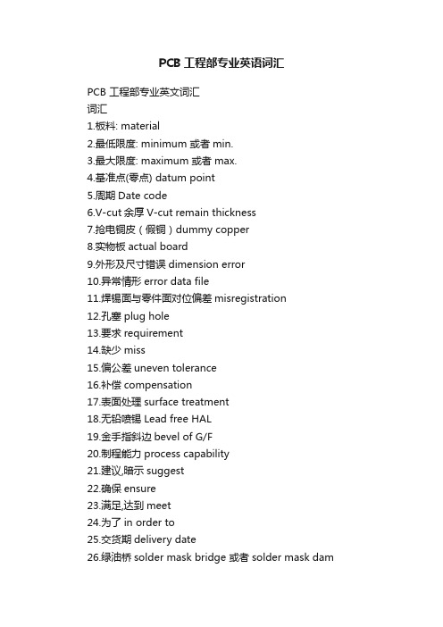
PCB工程部专业英语词汇
PCB工程部专业英语词汇PCB 工程部专业英文词汇词汇1.板料: material2.最低限度: minimum 或者min.3.最大限度: maximum 或者max.4.基准点(零点) datum point5.周期Date code6.V-cut余厚V-cut remain thickness7.抢电铜皮(假铜)dummy copper8.实物板actual board9.外形及尺寸错误dimension error10.异常情形error data file11.焊锡面与零件面对位偏差misregistration12.孔塞plug hole13.要求requirement14.缺少miss15.偏公差uneven tolerance16.补偿compensation17.表面处理surface treatment18.无铅喷锡Lead free HAL19.金手指斜边bevel of G/F20.制程能力process capability21.建议,暗示suggest22.确保ensure23.满足,达到meet24.为了in order to25.交货期delivery date26.绿油桥solder mask bridge 或者solder mask dam27.根据according to28.单边3mil per side 3 mil29.直径diameter30.半径radius 31.小于3mil less than 3mil32.高于3mil more than 3 mil33.压合结构stacking structure 或者stack_up34.附件:attached file35.样品:sample36.文档:Document37.答复:answer; reply38.规格:spec39.与...同样的:the same as40.前版本:previous version(old version)41.生产:production42.确认:confirm43.再次确认:confirm again44.工程问题:engineering query(EQ)45.尽快:as soon as possible46.生产文件:production Gerber47.联系某人:contact somebody48.提交样板:submit sample49.交货期:delivery date50.电测成本:ET(electrical test)cost51.通断测试:Open and short testing52.参考:refer to53.IPC标准:IPC standard54.IPC二级:IPC class 255.可接受的:acceptable56.允许:permit57.制造:manufacture 或者fabricate58.修改:revision59.公差:tolerance60.忽略:ignore61.工具孔:tooling hole62.安装孔:mounting hole63.元件孔:component hole64.槽孔:slot hole65.邮票孔:snap off hole 或者stamp hole66.导通孔:via hole67.盲孔:blind via hole68.埋孔:buried via hole69.金属化孔:PTH(plated through hole)70.非金属化孔:NPTH( no plated through hole)71.孔位:hole location72.避免:avoid73.原设计:original design74.修改:modify75.按原设计:follow up original design76.附边:waste tab, waste area 或者breakaway tab77.铜条:copper strip78.拼板:panel drawing79.板厚:board thickness80.删除:remove(delete)81.削铜:shave the copper82.露铜:copper exposure 或者exposed copper83.光标点: fiducial mark84.不同:be different from(differ from)85.内弧:inside radius86.焊环:annular ring87.单板尺寸:single size88.拼板尺寸:panel size89.铣,锣:routing90.铣刀:router 或者Routing bit91.楔形掏槽V-cut 或者V scoring92.哑光:matt93.光亮的:glossy94.锡珠:solder ball(solder plugs)95.阻焊:solder mask(solder resist)96.阻焊开窗:solder mask opening 97.单面开窗:single side mask opening98.补油:touch up solder mask99.补线:track welds100.毛刺:burrs101.去毛刺:deburr102.镀层厚度:plating thickness103.清洁度:cleanliness104.离子污染:ionic contamination105.阻燃性等级:flammability retardant rating 106.黑化:black oxidation107.棕化:brown oxidation108.红化:red oxidation109.可焊性不良:poor solderability110.焊料:solder111.包装:packaging112.角标:corner mark113.特性阻抗:characteristic impedance 114.正像:positive 115.负片:negative116.镜像:mirror117.线宽:line width 或者trace width118.线距:line spacing 或者trace spacing 119.做样:buildsample120.按照:according to121.成品:finished122.做变更:make the change123.相类似:similar to124.规格:specification125.下移:shift down126.垂直地:vertically127.水平的:horizontally128.增大:increase129.缩小:decrease130.表面处理:Surface Finishing131.波峰焊:wave solder132.钻孔数据:drilling data133.标记:Logo134.Ul 标记:UL logo,或者Ul Marking135.蚀刻标记:etched marking136.周期:date code137.翘曲:bow and twist138.外层:outer layer 或者external layer139.内层:inner layer 或者internal layer140.顶层:top layer141.底层:bottom layer142.元件面:component side143.焊接面:solder side144.阻焊层:solder mask layer145.字符层:legend layer (silkscreen layer or over layer) 146.兰胶层:peelable SM layer147.贴片层:paste mask layer148.碳油层:carbon layer149.外形层:outline layer(profile layer)150.白油:white ink151.绿油:green ink152.喷锡:hot air leveling (HAL)153.电金,水金:flash gold154.插头镀金:plated gold edge-board contacts155.金手指:Gold-finger156.防氧化:Entek (OSP)157.沉金:Immersion gold (chem. Gold)158.沉锡:Immersion Tin(chem.Tin)159.沉银:Immersion Silver (chem. silver)160.单面板:single sided board161.双面板:double sided board162.多层板:multilayer board 163.刚性板:rigid board164.挠性板:flexible board165.刚挠板:flex-rigid board166.铣:CNC (mill , routing)167.冲:punching168.倒角:beveling169.斜面:chamfer170.倒圆角:fillet171.尺寸:dimension172.材料:material173.介电常数:Dielectric constant 174.菲林:film175.成像:Imaging176.板镀:Panel Plating177.图镀:Pattern Plating178.后清洗:Final Cleaning179.叠层:stacking structure (stack-up) 180.污染焊盘:contaminate pad181.分孔图:drill chart 或者drill map 182.度数:degree183.被…覆盖:be covered with184.负公差:minus tolerance185.标靶盘:target pad186.外形公差:routing tolerance 187.芯板:core188.半固化片Prepreg189.阻抗线:impedance trace190.评估estimate191.玻纤显露Fiber Exposure192.底铜base copper193.工作搞working Gerber194.原稿original art work195.放宽relax196.挖空blanking 或者cut-out197.一般性阻焊油墨general resist ink198.孔位错误mis hole location199.压合周期press cycle200.毛边serrated edges201.跳印skip printing202.气泡blistering203.隔离焊盘isolated pad204.泪滴tear drops205.箭头arrows206.加大Enlarge207.压合周期press cycle208.毛边serrated edges209.跳印,漏印skip printing210.宽度与厚度的比值width-to-thickness ratio 211.调整adjust212.铜箔基板copper claded laminates213.线路露铜copper exposure214.孔内异物dirty hole215.椭圆形elliptical set216.纤维突出fiber protrusion217.填充料filler218.互相连通interconnection219.改善方案implementation220.板料使用率material use factor221.回路,网络network222.缺口nick223.氧化oxidation224.剥离(剥落) peeling off225.补线不良poor touch-up226.品质等级quality classification227.对位孔registration228.拒收rejectable 229.树脂含量resin content230.排列电阻resistor network231.锣刀(铣刀)routing bit232.孔内沾文字S/L on hole233.孔内绿漆S/M on hole234.线路沾锡solder on trace235.金手指沾锡solder on G/F236.废框scrap237.封孔处理sealing238.间距不足spacing non-enough 239.靶位孔target hole240.测试线路test circuit241.热应力试验thermal stress242.厚度分布thickness distribution 243.薄基板,内层板thin core244.线路缺口及针孔track nick & pin hole 245.裁切线trim line246.真平整true leveling247.真正位置的孔true position248.万用型universal249.气化室vaporizer250.仓库warehouse251.契尖角wedge angle252.线细width reduce253.良率yield254.渗铜,渗入,灯芯效应wicking255.允收acceptable256.试样点coupon location257.经核准的,被认可的approved258.超越胜过,超过其他exceed259.牛皮纸kraft paper260.孔壁破铜Hole void261.孔位破出Hole breakoutPCB生产—经典流程—英文培训教程A. 开料( Cut Lamination)a-1 裁板( Sheets Cutting)a-2 原物料发料(Panel)(Shear material to Size) B. 钻孔(Drilling)b-1 内钻(Inner Layer Drilling )b-2 一次孔(Outer Layer Drilling )b-3 二次孔(2nd Drilling)b-4 雷射钻孔(Laser Drilling )(Laser Ablation ) b-5 盲(埋)孔钻孔(Blind & Buried Hole Drilling) C. 干膜制程( Photo Process(D/F))c-1 前处理(Pretreatment)c-2 压膜(Dry Film Lamination)c-3 曝光(Exposure)c-4 显影(Developing)c-5 蚀铜(Etching)c-6 去膜(Stripping)c-7 初检( Touch-up)c-8 化学前处理,化学研磨( Chemical Milling )c-9 选择性浸金压膜(Selective Gold Dry Film Lamination) c-10 显影(Developing )c-11 去膜(Stripping )Developing , Etching & Stripping ( DES )D. 压合Laminationd-1 黑化(Black Oxide Treatment)d-2 微蚀(Microetching)d-3 铆钉组合(eyelet )d-4 叠板(Lay up)d-5 压合(Lamination)d-6 后处理(Post Treatment)d-7 黑氧化( Black Oxide Removal ) d-8 铣靶(spot face)d-9 去溢胶(resin flush removal)E. 减铜(Copper Reduction)e-1 薄化铜(Copper Reduction)F. 电镀(Horizontal Electrolytic Plating)f-1 水平电镀(Horizontal Electro-Plating) (Panel Plating) f-2 锡铅电镀( Tin-Lead Plating ) (Pattern Plating)f-3 低于1 mil ( Less than 1 mil Thickness )f-4 高于1 mil ( More than 1 mil Thickness)f-5 砂带研磨(Belt Sanding)f-6 剥锡铅( Tin-Lead Stripping)f-7 微切片( Microsection)G. 塞孔(Plug Hole)g-1 印刷( Ink Print )g-2 预烤(Precure)g-3 表面刷磨(Scrub)g-4 后烘烤(Postcure)H. 防焊(绿漆/绿油): (Solder Mask)h-1 C面印刷(Printing Top Side)h-2 S面印刷(Printing Bottom Side)h-3 静电喷涂(Spray Coating)h-4 前处理(Pretreatment)h-5 预烤(Precure)h-6 曝光(Exposure)h-7 显影(Develop)h-8 后烘烤(Postcure)h-9 UV烘烤(UV Cure)h-10 文字印刷( Printing of Legend )h-11 喷砂( Pumice)(Wet Blasting)h-12 印可剥离防焊(Peelable Solder Mask)I . 镀金Gold platingi-1 金手指镀镍金( Gold Finger )i-2 电镀软金(Soft Ni/Au Plating)i-3 浸镍金( Immersion Ni/Au) (Electroless Ni/Au) J. 喷锡(Hot Air Solder Leveling)j-1 水平喷锡(Horizontal Hot Air Solder Leveling) j-2 垂直喷锡( Vertical Hot Air Solder Leveling)j-3 超级焊锡(Super Solder )j-4. 印焊锡突点(Solder Bump)K. 成型(Profile)(Form)k-1 捞型(N/C Routing ) (Milling)k-2 模具冲(Punch)k-3 板面清洗烘烤(Cleaning & Backing)k-4 V型槽( V-Cut)(V-Scoring)k-5 金手指斜边( Beveling of G/F)L. 开短路测试(Electrical Testing) (Continuity & Insulation Testing) l-1 AOI 光学检查( AOI Inspection)l-2 VRS 目检(Verified & Repaired)l-3 泛用型治具测试(Universal Tester)l-4 专用治具测试(Dedicated Tester)l-5 飞针测试(Flying Probe)M. 终检( Final Visual Inspection)m-1 压板翘( Warpage Remove)m-2 X-OUT 印刷(X-Out Marking)m-3 包装及出货(Packing & shipping)m-4 目检( Visual Inspection)m-5 清洗及烘烤( Final Clean & Baking)m-6 护铜剂(ENTEK Cu-106A)(OSP)m-7 离子残余量测试(Ionic Contamination Test )(Cleanliness Test)m-8 冷热冲击试验(Thermal cycling Testing)m-9 焊锡性试验( Solderability Testing )N. 雷射钻孔(Laser Ablation)N-1 雷射钻Tooling孔(Laser ablation Tooling Hole)N-2 雷射曝光对位孔(Laser Ablation Registration Hole)N-3 雷射Mask制作(Laser Mask)N-4 雷射钻孔(Laser Ablation) N-5 AOI 检查及VRS ( AOI Inspection & Verified & Repaired) N-6 Blaser AOI (after Desmear and Microetching)N-7 除胶渣(Desmear)N-8 微蚀(Microetching )。
PCB缺陷英文对照

PCB缺陷中文名称
漏印字符 金粗 金簿 金手指缺口 金手指发黑 字符印反 金手指针孔 标志不清 标志错 绿油鬼影 手指印 补线不良 锡高 孔小 字符错 字符印偏 字符入孔 字符 重影 漏镀金手指 金手指发白 焊盘脱落 焊盘露铜 断绿油桥 塞孔 水迹 锡珠 砂孔 油薄 聚油 锡粗 线路上锡 绿油下杂物 焊盘损坏 焊盘翘起 偏位 漏钻孔 焊盘缺口 线路缺口 返工不良 绿油下氧化 焊盘翘起 漏钻孔 露布纹 钻偏孔 孔损害 基材分层 蚀刻过度 多孔 残铜 孔内露基材 焊盘脱落 焊盘凹痕 焊盘凸起 焊盘损坏 焊盘缺口 焊盘露铜 修理不良 铜薄 内层擦花
英文对照
skip Au too big Au too thin G/F voids/nick on G/F G/F too black inverse C/M G/F pinholes symbol unclear symbol wrong ghost in S/M finger print poor line repairing exessive solder hole undersize wrong C/M C/M misalignment C/M in hole C/M doubloe image missing plating G/F G/F gray pad break off/pad peel off pad expose cu missing S/M bridge block hole water print solder ball pitting
poor repairing s/m
pinhole paster stain burrs in hole solder in hole expose Cu expose Ni solder mask blister solder mask winbles G/F oxiding Au discoloration Au surface blister solder mask in hole board angle damafe warp open circuit short circuit circuit wist circuit nick circuit dent plating Bloody pad nick I/L white spot poor B.O measling pinking ring press blister misregistation shift no Cu on Pth hole burrs Cu on NPTH exposed laminate dent on Cu surface
- 1、下载文档前请自行甄别文档内容的完整性,平台不提供额外的编辑、内容补充、找答案等附加服务。
- 2、"仅部分预览"的文档,不可在线预览部分如存在完整性等问题,可反馈申请退款(可完整预览的文档不适用该条件!)。
- 3、如文档侵犯您的权益,请联系客服反馈,我们会尽快为您处理(人工客服工作时间:9:00-18:30)。
WINDOWS不能軟體關機 QAPLUS 當機 音效不良 VGA不良或螢冪雜訊 USB不良 凹痕
英文 CACHE MEMORY defect cann't read floppy IDE1 cann't read or error KEYBOARD LOCK error GspReEeEdNeerrroror ror cann't switch LED no light or error speaker error or disorder COM 1/2 defect LPT1 defect CMOS setting error time stopped ID 00 defect CARD defect WINDOWS hang up WINDOWS cann't boot from software QAPLUS hang up audio error VGA error or disorder USB defect sink mark
電源短路 CPU速度不對 MEMORY不良 KEYBOARD不良 HIMEM ERROR或當機 凹孔 條狀痕 表面裂痕 橘皮狀表皮皺摺粗糙 波動 冒汗 扭曲 翹曲 波痕 熔塌 焊痕 白化 皺紋
pock mark resin streak resin wear riding sagging saponification scar scrap scrap jam scratch scuffing seam shock line short shot
英文 PCB defect soldering open short missing wrong component invert position shift component shift reverse tombstone component side up solder ball extra soldering poor soldering bar code defect
痘斑 樹脂流紋 樹脂脫落 凹陷 松垂 皂化 疤痕 廢料 廢料阻塞 刮傷/劃痕 深沖表面劃傷 裂痕 模口擠痕 充填不足
英文 mixed boards mixed versions component lead float illegible character float lead knee down lead doesn't penetrate incoming matrials defect lead longer solder hole solder splash solder tail extra soldering non-wetting hole clog
常見不良現象中英文對照表
英文 poor solder mask PAD defect forming defect board bent extra component component deform ICT test fail voltage defect no voltage wire open no boot BIOS flash error cann't flash BIOS cann't RESET battery no voltage
中文 防焊不良 PAD不良 成型不良 板彎板翹 多件 零件變形 ICT測試不良 電壓不良 無電壓顯示 燒斷線 不開機 BIOS燒錄不良 不能燒BIOS 不能RESET 電池沒電
常見不良現象中英文對照表
cold soldering reverse bounding defect component crash circuit defect skin inclusion galling glazing gloss grease pits grinding defect haircrack haze incrustation indentation internal porosity mismatch mottle necking nick orange peel overflow peeling pit pitting corrosion plate mark pock
中文 混板 混版 零件翹腳 文字面不良 浮高 折腳 腳未出 原材不良 腳長 錫洞 錫渣 錫尖 包焊 拒焊 孔塞
residue flux PCB surface dirty component broken overflowing component oxidized straightening aberration atomization bank mark bite blacking hole blacking scab blister blooming blushing body wrinkle breaking-in bubble burn mark burr burr(金屬) flash(塑件) camber center buckle check checking chipping clamp-off
G/F dent G/F scratch G/F residue glue G/PCB不良 空焊 短路 缺件 錯件 反向 位移 偏移 翻面 立碑 側立 錫球 錫多 吃錫不良 條碼不良
殘留助焊劑 板面不澍 零件破損 溢錫 零件氧化 矯直 色差 霧化 凸料紋 咬入 塗料孔(鑄疵) 塗料疤 起泡 起霜 泛白 皺紋 冒口帶肉 膜泡 糊斑 毛邊 毛邊 翹曲 表面中部波皺 細裂痕 龜裂 修整表面缺陷 鑄件凹痕
冷焊 反白 點膠不良 撞件 線路不良 表皮摺疊 毛邊 光滑 光澤 汙斑 磨痕 發裂 霧度 水銹 壓痕 內部氣孔 偏模/不吻合 斑點 縮頸 割痕 橘皮狀表面缺陷 溢流 剝離 坑 點狀腐蝕 模板印痕 麻點
塌陷 色斑 腐蝕 裂痕 龜裂 變形 切邊碎片 裂邊 退色 填充料斑 裂紋 凸緣起皺 刮傷 流痕
collapse color mottle corrosion crack crazing deformation edge edge crack fading filler speak fissure flange wrinkle flaw flow mark
中文 CACHE MEMORY不良 A磁碟機不讀 IDE1硬碟機不讀或不抓 KEYBOARD LOCK不良 GREEN不良 速度不對或不能切換 LED燈不亮或不良 喇叭不叫或亂叫 COM 1/2不良 LPT1不良 CMOS設定不良 時間不動 ID 00不良 CARD不良 WINDOWS當機
power short CPU frequency error MEMORY defect KEYBOARD defect HIMEM ERROR or hang up shrinkage pool streak surface check surface roughening surging sweat out torsion warpage waviness webbing weld mark whitening wrinkle
英文 Game Port defect cann't burn in Lan number Lan function test error 1394 error AMR FAIL CNR FAIL BEAR ERROR NUMBER LCD ERROR leakage current ACPI detect error Case Open defect SCR defect CHIP ID ERROR others G/F adhere stannum
中文 Game Port不良 不能燒網路號碼 網絡功能不良 1394不良 AMR FAIL CNR FAIL BEAR ERROR NUMBER LCD ERROR 漏電流 ACPI 偵側不良 Case Open不良 SCR不良 CHIP ID ERROR 其他 金手指沾錫
金手指凹陷 金手指刮傷 金手指殘膠 金手指缺口