P87LPC760 OTP单片机数据手册
cd4094 芯片驱动两个芯片驱动两个芯片驱动两个pdf
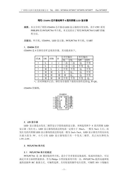
利用CD4094芯片驱动两个8段共阴极LED显示器摘要本文介绍了利用CD4094芯片驱动LED显示器的应用实例其中CPU采用PHILIPS的P87LPC764单片机本文还给出了利用P87LPC764 UART的编程方法关键词单片机CD4094LED显示器P87LPC764单片机UART1CD4094芯片CD4094是8位移位存贮总线寄存器其功能表如下并行输出串行输出CLK OE STR DQ1Q n QS*Q`SL三态三态Q不变L三态三态不变Q7H L不变不变Q不变Q7不变H H L L QQ7不变H H H H QH H H不变不变不变Q7*在时钟脉冲正沿移位寄存器第7级的内容传送到Q 8 和QSCD4094管脚图2LED显示器LED显示器是由发光二极管显示字段组成的显示器本例选用两个8段共阴极LED显示器发红光LED显示器每段流过的电流一定要小于30mA一般为5mA左右而发红光的共阴极LED显示器每段流过的电流一般为2mA~7mA LED显示器允许的反向电压最大值为5V小尺寸的LED显示器每段只有一个发光二极管其正向压降约为1.5V~2.0V3P87LPC764单片机3.1 P87LPC764单片机概述P87LPC764是20脚封装的单片机适合于许多要求高集成度低成本的场合可以满足许多方面的性能要求作为Philips小型封装系列中的一员P87LPC76x提供高速和低速的晶振和RC振荡方式可编程选择具有较宽的操作电压范围可编程I/O口线输出模式选择可选择施密特触发输入LED驱动输出有内部看门狗定时器P87LPC76x采用80C51加速处理器结构指令执行速度是标准80C51 MCU的两倍P87LPC764拥有4K 字节的OTP程序存储器128字节的SRAM P87LPC764具有全双工通用异步接收/发送器3.2 P87LPC764的I/O口P87LPC76x有3组I/O端口Port0Port1和Port2I/O数量取决于振荡和复位方式选择当选用两个口线作为外部振荡器和一个外部复位时P87LPC76x可使用15个I/O口如果选用片内振荡和内部复位时可使用多达18个脚作为I/O口线除了3个I/O口P1.2P1.3P1.5以外其他所有的P87LPC76x均可由软件配置成4种输出类型之一如下表所示四种输出类型分别为准双向口(标准8051输出模式)上拉开漏输出和仅有输入由2个I/O口控制寄存器控制每个I/O口输出类型所有口线均有20mA的驱动能力可以直接驱动LED显示器I/O口控制寄存器PxM1.Y PxM2.Y I/O口输出模式00准双向口01上拉10仅为输入11开漏3.3 P87LPC764的UARTP87LPC76x内含加强型80C51 全双工通用异步接收/发送器UART模式1及模式3时定时器1作为波特率可变模式0及模式2时波特率固定由于P87LPC76xMCU时钟不同于标准80C51波特率计算亦有不同在标准80C51 UART基础上增加了帧错误检测及地址识别串行端口是全双工的即它可同时发送及接收同时带有接收缓冲所以前一接收字节从SBUF寄存器内读出之前可开始接收下一字节但是如果下一字节接收完毕而前一字节仍未读出则前一字节将被丢失串行端口接收及发送寄存器均通过SBUF访问对SBUF 写操作则装入发送寄存器读SBUF则访问一个物理上分开的接收寄存器在本篇应用实例中将使用UART模式0实现P87LPC764与CD4094的串行通信在UART模式0方式时串行数据通过RxD进出TxD输出时钟每次发送或接收以LSB低位作首位每次8位波特率固定为MCU时钟频率的1/6串行口控制寄存器SCONSCON地址98H76543210可位寻址复位值00H SM0/FE SM1SM2REN TB8RB8TI RI位符号SCON.7FE功能帧错误当检测到一个无效停止位时通过UART接收器设置该位但它必须由软件清零在PCON寄存器中的SMOD0位必须设置为1SCON.7SM0和SM1定义串行口操作模式在PCON寄存器中的SMOD0必须设置为0SCON.6SM1和SM0定义串行口操作模式见下表其中UART为通用异步接收和发送器的英文缩写fosc为振荡器频率SM0 SM1UART模式波特率0 00同步移位寄存器Fosc/60 118位UART 可变1 029位UART Fosc/32或Fosc/161 139位UART UART可变SCON.5 SM2在模式2和3中多处理机通信使能位在模式2或3中若sm2=1且接收到的第9位数据RB8是0则RI接收中断标志不会被激活在模式1中若sm2=1且没有接收到有效的停止位则RI不会被激活在模式0中sm2必须是0SCON.4REN允许接收位由软件置位或清除REN=1时允许接收REN=0时禁止接收SCON.3TB8模式2和3中发送的第9数据可以按需要由软件置位或清除SCON.2RB8模式2和3中已接收的第9位数据在模式1中或sm2=0RB8是已接收的停止位在模式0中RB8未用SCON.1TI发送中断标志在模式0中在发送完第8位数据时由硬件置位在其它模式在发送停止位之初由硬件置位在任何模式中都必须由软件来清除TISCON.0RI接收中断标志在模式0中接收第8位结束时由硬件置位在其它模式中在接收停止位的半中间由硬件置位在任何模式除SM2必须由软件清除RI4电路图本例的电路图参见下页5软件设计5.1程序清单参见下页5.2子程序使用说明5.2.1 显示子程序使用说明标号DISPLAY功能把DISPLAY_DATA 中的初始数显示到LED1-LED2十位数值显示到LED1个位数值显示到LED2当十位数值为0时LED1不显示每个数值的显示时间由DISPLAY_TIME确定当显示到99之后返回调用处入口条件显示初始数在DISPLAY_DATA中每个数值的显示时间在DISPLAY_TIME 中出口信息无调用低级子程序SEND_4094DELAY_10ms影响资源Acc R2R3R7B DPTR5.2.2 传送数据给CD4094子程序使用说明标号SEND_4094功能传送一个字节数给CD4094利用UART模式0入口条件所要传送的数在Acc中出口信息无调用低级子程序无影响资源特殊功能寄存器SCON SBUF标志位TI5.2.3 延时10ms子程序使用说明标号DELAY_10ms功能延时10ms入口条件无出口信息无调用低级子程序无影响资源R5R6参考文献1<<P87LPC76x OTP 单片机使用指南>> 周立功岳宪臣等编广州周立功单片机发展有限公司 2000.12<<MCS-51系列单片机应用系统设计>> 何立民北京航空航天大学出版社 1990.1 3<<单片微机测控系统设计大全>> 王福瑞等编北京航空航天大学出版社 1998.4 4<<通用集成电路速查手册>> 宋春荣等编山东科学技术出版社 1995.1利用CD4094驱动两个8段共阴极LED显示器CPU选用P87LPC764****************************************************************************硬件使用一个CD4094两个8段LED显示器共阴极P87LPC764的4个I/O口以及八个270的电阻程序说明下面程序运用UART模式0实现P87LPC764与 CD4094的数据传送并把数据显示到两个8段LED显示器共阴极****************************************************************************CLK_4094 EQU P1.0TxD 端口DATA_4094EQU P1.1RxD 端口LED1_SELECT EQU P0.0LED1位选0有效LED2_SELECT EQU P0.1LED2位选0有效DISPLAY_DATA DATA30H显示数据缓冲区DISPLAY_TIME DATA31H显示时间间隔缓冲区P0M1EQU84H端口模式选择SFR总共4个P0M2EQU85HP1M1EQU91HP1M2EQU92HORG0000HAJMP RESET程序初始化----------------------------------------------------------子程序----------------------------------------------------------ORG0080H;----------------------------------------------------------标号SEND_4094功能把Acc中的数据传送给CMOS4094入口传送的数据在Acc中出口数据传送到P1.1 (RxD 端口)--------------------------------------------------------SEND_4094:MOV SCON,#00H设置UART模式0MOV SBUF,A传送的数据送到SBUFJNB TI,$等待发送一个字节CLR TI清除发送中断标志位RET返回--------------------------------------------------标号DELAY_10ms功能延时10ms时钟6MHz,倍频入口无出口无--------------------------------------------------DELAY_10ms:MOV R5,#32HDELAY_10ms1:MOV R6,#64HDJNZ R6,$DJNZ R5,DELAY_10ms1RET-----------------------------------------------------------------------------标号DISPLAY功能把DISPLAY_DATA 中的数据显示到两个8段LED显示器如果Acc的高四位等于0则不显示显示时间用完时显示下一个递增数据显示到99时返回入口显示初始数据在DISPLAY_DATA 中显示时间间隔在DISPLAY_TIME 中出口无-----------------------------------------------------------------------------DISPLAY:MOV R4,DISPLAY_TIME保存显示时间间隔MOV A,DISPLAY_DATA保存显示数据MOV R2,AANL A,#0FHMOV R7,ACJNE R7,#0AH,DIS_1Acc的低四位等于10不等于则跳转MOV A,R2如果等于则加05HADD A,#05HMOV DISPLAY_DATA,A保存数据AJMP DIS_2继续显示数据DIS_1:MOV B,AMOV A,R2SWAP AANL A,#0FHMOV R2,A保存显示数据的高四位MOV R3,B保存显示数据的低四位JNZ DISPLAY_LOOP显示数据的高四位等于0不等于则跳转MOV R2,#0AH等于0则不显示DISPLAY_LOOP:MOV A,R2MOV DPTR,#DISPLAY_CODEMOVC A,@A+DPTRACALL SEND_4094CLR LED1_SELECT打开LED1显示器ACALL DELAY_10ms延时10msSETB LED1_SELECT关闭LED1显示器MOV A,R3MOV DPTR,#DISPLAY_CODEMOVC A,@A+DPTRACALL SEND_4094CLR LED2_SELECT打开LED2显示器ACALL DELAY_10ms延时10msSETB LED2_SELECT关闭LED2显示器DJNZ R4,DISPLAY_LOOP显示时间用完DIS_2:INC DISPLAY_DATA 取下一个显示数据MOV A,DISPLAY_DATACJNE A,#0A0H,DISPLAY下一个显示数据等于100等于则返回RET---------------------------------------------------LED显示器的显示代码---------------------------------------------------DISPLAY_CODE:DB0FCH0DB60H1DB0DAH2DB0F2H3DB66H4DB0B6H5DB0BEH6DB0E0H7DB0FEH8DB0F6H9DB00H全灭****************************************************************主程序**************************************************************** RESET:初始化程序MOV SP,#60HMOV P0M1,#00H设置端口模式MOV P0M2,#00HSETB P0.0关闭LED1显示器SETB P0.1关闭LED2显示器MAIN:MOV DISPLAY_DATA,#00H设置显示初始数据MOV DISPLAY_TIME,#32H设置数据显示时间间隔ACALL DISPLAY开始显示AJMP RESET重复操作ENDCD4094芯片驱动两个8段LED显示器电路原理图。
数据手册_HR7P187_Datasheet_C V2.1

加强描述:3.2.3,5.1.4,6.1.3,6.5.1,6.5.2, 附录 1.1,附录 2.1,附录 2.2
错误修正:2.1,2.2,4.3,5.1.1.1,5.1.1.2,5.1.2.1, 5.1.2.2,5.4.3,附录 1.3,附录 1.4
V2.1 版权所有©上海海尔集成电路有限公司
4/85
V2.1 版权所有©上海海尔集成电路有限公司
3/85
上海海尔集成电路有限公司
HR7P187 数据手册
版本 V1.0 V2.0
V2.1
修改日期 2010-08-02 2011-03-11
2011-04-26
修订历史
预发行版
更改概要
添加内部时钟电气特性及部分补充说明
2/85
上海海尔集成电路有限公司
HR7P187 数据手册
产品订购信息
型号
程序存储器
HR7P187F4R HR7P187F4R-B
HR7P187F4D HR7P187F4D-B FLASH:2K×15 位
HR7P187F4S HR7P187F4S-B
数据存储器
版权所有©
上海海尔集成电路有限公司
本数据手册的信息在发行时是经过核实并且尽最大努力使之精确的。上海海尔集成电路有限公司不为由于使用本数 据手册而可能带来的风险或后果负责。手册中的实例仅作为说明用途,上海海尔集成电路有限公司不担保或确认这 些实例是合适的、不需进一步修改的、或推荐使用的。上海海尔集成电路有限公司保留不需要通知本数据手册读者 而修改自己产品的权利。如需得到最新的产品信息,请随时用上述联系方式与上海海尔集成电路有限公司联系。
上海海尔集成电路有限公司
HR7P187 数据手册
LPC-P1227开发板用户手册说明书

LPC-P1227LPC-P1227 development board USER’S MANUALInitial release, March 2012Designed by OLIMEX Ltd, 2011All boards produced by Olimex LTD are ROHS compliantOLIMEX© 2012LPC-P1227 User's ManualDisclaimer:© 2012 Olimex Ltd. Olimex®, logo and combinations thereof, are registered trademarks of Olimex Ltd. Other terms and product names may be trademarks of others.The information in this document is provided in connection with Olimex products. No license, express or implied or otherwise, to any intellectual property right is granted by this document or in connection with the sale of Olimex products.Neither the whole nor any part of the information contained in or the product described in this document may be adapted or reproduced in any material from except with the prior written permission of the copyright holder.The product described in this document is subject to continuous development and improvements.All particulars of the product and its use contained in this document are given by OLIMEX in good faith. However all warranties implied or expressed including but not limited to implied warranties of merchantability or fitness for purpose are excluded. This document is intended only to assist the reader in the use of the product. OLIMEX Ltd. shall not be liable for any loss or damage arising from the use of any information in this document or any error or omission in such information or any incorrect use of the product.Thank you for purchasing LPC-P1227 development board assembled byOLIMEX LTDOLIMEX© 2012LPC-P1227 User's ManualTable of ContentsCHAPTER 1 (5)OVERVIEW (5)1. Introduction to the chapter (5)1.1 Features (5)1.2 Organization (6)CHAPTER 2 (7)SETTING UP THE LPC-P1227 BOARD (7)2. Introduction to the chapter (7)2.1 Electrostatic warning (7)2.2 Requirements (7)2.3 Powering the board (7)2.4 Prebuilt software (8)CHAPTER 3 (9)LPC-P1227 BOARD DESCRIPTION (9)3. Introduction to the chapter (9)3.1 Layout (top view) (9)CHAPTER 4 (10)THE LPC1227FBD64 MICROCONTROLLER (10)4. Introduction to the chapter (10)4.1 The microcontroller (10)CONTROL CIRCUITY (12)5. Introduction to the chapter (12)5.1 Reset (12)5.2 Clocks (12)CHAPTER 6 (13)HARDWARE (13)6. Introduction to the chapter (13)6.1 PWR Connector (13)6.2 SWD1 connector (13)6.3 SWD2 Header (14)6.4 UEXT (14)6.5 Pads on the proto area (16)6.6 RS232 Null-modem connector (17)6.7 Jumper description (18)6.8 LCD Display (19)OLIMEX© 2012LPC-P1227 User's Manual6.9 Additional hardware components (19)CHAPTER 7 (20)MEMORY AND BLOCK DIAGRAM (20)7. Introduction to the chapter (20)7.1 Memory organization (21)CHAPTER 8 (22)SCHEMATICS (22)8. Introduction to the chapter (22)8.1 Eagle schematic (22)8.2 Physical dimensions (24)CHAPTER 9 (25)REVISION HISTORY (25)9. Introduction to the chapter (25)9.1 Document revision (25)9.2 Web page of your device (25)OLIMEX© 2012LPC-P1227 User's ManualCHAPTER 1OVERVIEW1. Introduction to the chapterThank you for choosing the LPC-P1227 development board from Olimex! This document provides a User’s Guide for the Olimex LPC-P1227 development board. As an overview, this chapter gives the scope of this document and lists the board’s features. The document’s organization is then detailed.The LPC-P1227 development board enables code development of applications running on the LPC1227 Cortex-M0 microcontroller, manufactured by NXP Semiconductors.1.1 Features•MCU: LPC1227 Cortex-M0, up to 45Mhz, 128 kB Flash, 8kB SRAM, 2 UARTs , SPI, I2C,10 bit ADC•RS232•Buzzer•NOKIA 3310 LCD•12 MHz crystal resonator•Power supply circuit•Power-on LED•Debug interface – SWD (Serial Wire Debug)•UEXT connector•Two user leds•Three user buttons•Reset button•Prototype area•FR-4, 1.5 mm, soldermask, component print•Dimensions:80x50mm (3.15 x 1.97")OLIMEX© 2012LPC-P1227 User's Manual 1.2 OrganizationEach section in this document covers a separate topic, organized as follow:–Chapter 1 is an overview of the board usage and features–Chapter 2 provides a guide for quickly setting up the board–Chapter 3 contains the general board diagram and layout–Chapter 4 describes the component that is the heart of the board: the LPC1227FBD64 microcontroller–Chapter 5 is an explanation of the control circuitry associated with the microcontroller to reset. Also shows the clocks on the board–Chapter 6 covers the connector pinout, peripherals and jumper description–Chapter 7 shows the processor diagram and memory map–Chapter 8 provides the schematics–Chapter 9 contains the revision historyOLIMEX© 2012LPC-P1227 User's ManualCHAPTER 2SETTING UP THE LPC-P1227 BOARD2. Introduction to the chapterThis section helps you set up the LPC-P1227 development board for the first time.Please consider first the electrostatic warning to avoid damaging the board, then discover the hardware and software required to operate the board.The procedure to power up the board is given, and a description of the default board behavior is detailed.2.1 Electrostatic warningLPC-P1227 is shipped in a protective anti-static package. The board must not be exposed to high electrostatic potentials. A grounding strap or similar protective device should be worn when handling the board. Avoid touching the component pins or any other metallic element.2.2 RequirementsIn order to set up and program the LPC-P1227, the following items are required:- A source of power – the board can be powered through the PWR jack or through the SWD-1 (SWD-2) interface- In order to program the board you will need a programmer that supports SWD (Serial Wire Debug) interfaceAlso, a host-based software toolchain is required in order to program/debug the LPC-P1227 board. There are also a number of ready IDEs available like IAR Embedded Workbench,Rowley CrossWorks, Code Composer Studio, etc.The only low cost Olimex option at the time writing this guide is available if you use Rowley's Crossworks IDE. You can get any of our ARM-USB debuggers + ARM-JTAG-SWD adapter. As of moment of writing this guide OpenOCD 0.5.0 doesn't support SWD flashing.2.3 Powering the board- Provide between 5V and 9V to the board's PWR jackOLIMEX© 2012LPC-P1227 User's ManualOR- Connect your SWD debugger2.4 Prebuilt softwareOn powering the board the PWR LED should turn on. LED1 and LED2 should start blinking alternatively. The LCD display shows 6 lines of text. You can connect the board to a PC via RS232 Null-modem interface. Then start your favourite terminal program at 115200, 8-N-1 and reset the board. A line with the statuses of 4 buttons (USER3, USER2, USER1, WAKE_UP) and ISP_E jumper appears. Press the buttons to see their state changing or change the jumper position. Pressing escape will disconnect the RS232.OLIMEX© 2012LPC-P1227 User's ManualCHAPTER 3LPC-P1227 BOARD DESCRIPTION3. Introduction to the chapterHere you get acquainted with the main parts of the board. Note the names used on the board differ from the names used to describe them. For the actual names check the LPC-P1227 board itself. 3.1 Layout (top view)CHAPTER 4THE LPC1227FBD64 MICROCONTROLLER4. Introduction to the chapterIn this chapter is located the information about the heart of LPC-P1227 – its microcontroller. The information is a modified version of the datasheet provided by its manufacturers.4.1 The microcontrollerMain processors features:•Processor core✗ARM Cortex-M0 processor, running at 45 MHz (one wait state from flash) or 30 MHz (zero wait states from flash). The LPC122x have a high score of over 45 in CoreMarkCPU performance benchmark testing, equivalent to 1.51/MHz.✗ARM Cortex-M0 built-in Nested Vectored Interrupt Controller (NVIC).✗Serial Wire Debug (SWD).✗System tick timer.•Memory✗8 kB SRAM.✗128 kB on-chip flash programming memory.✗In-System Programming (ISP) and In-Application Programming (IAP) via on-chip bootloader software.✗Includes ROM-based 32-bit integer division routines.•Clock generation unit✗Crystal oscillator with an operating range of 1 MHz to 25 MHz.✗12 MHz Internal RC (IRC) oscillator trimmed to 1 % accuracy that can optionally be used as a system clock.✗PLL allows CPU operation up to the maximum CPU rate without the need for a high-frequency crystal. May be run from the system oscillator or the internal RCoscillator.✗Clock output function with divider that can reflect the system oscillator clock, IRC clock, main clock, and Watchdog clock.✗Real-Time Clock (RTC).•Digital peripherals✗Micro DMA controller with 21 channels.✗CRC engine.✗Two UARTs with fractional baud rate generation and internal FIFO. One UART with RS-485 and modem support and one standard UART with IrDA.✗SSP/SPI controller with FIFO and multi-protocol capabilities.✗I2C-bus interface supporting full I2 C-bus specification and Fast-mode Plus with a data rate of 1 Mbit/s with multiple address recognition and monitor mode. I2C-buspins have programmable glitch filter.✗55 General Purpose I/O (GPIO) pins with programmable pull-up resistor, open-drain mode, programmable digital input glitch filter, and programmable input inverter.✗Programmable output drive on all GPIO pins. Four pins support high-current output drivers.✗All GPIO pins can be used as edge and level sensitive interrupt sources.✗Four general purpose counter/timers with four capture inputs and four match outputs (32-bit timers) or two capture inputs and two match outputs (16-bit timers).✗Windowed WatchDog Timer (WWDT); IEC-60335 Class B certified.•Analog peripherals✗One 8-channel, 10-bit ADC.✗Two highly flexible analog comparators. Comparator outputs can be programmed to trigger a timer match signal or can be used to emulate 555 timer behavior.•Power✗Three reduced power modes: Sleep, Deep-sleep, and Deep power-down.✗Processor wake-up from Deep-sleep mode via start logic using 12 port pins.✗Processor wake-up from Deep-power down and Deep-sleep modes via the RTC.✗Brownout detect with three separate thresholds each for interrupt and forced reset.✗Power-On Reset (POR).✗Integrated PMU (Power Management Unit).•Unique device serial number for identification.• 3.3 V power supplyFor comprehensive information on the microcontroller visit the NXP web page for a datasheet.At the moment of writing the microcontroller datasheet can be found at the following link:/products/lpc1000/datasheet/lpc122x.pdfCHAPTER 5CONTROL CIRCUITY5. Introduction to the chapterHere you can find information about reset circuit, power circuit and quartz crystal locations.5.1 ResetLPC-P1227 reset circuit includes R23 (10 KΩ), R24(330 Ω), LPC1227FB064 pin PIN40 (PIO0_13/RESET) and a RESET button.5.2 Clocks12 MHz quarz crystal Q1 is found at pins 1 and 2 of the processor.Real time clock (RTC) Q2 is connected to pins 57 and 58 of the processor.CHAPTER 6HARDWARE6. Introduction to the chapterIn this chapter are presented the connectors that can be found on the board all together with their pinout. Proto area is shown. Jumpers functions are described. Notes and info on specific peripherals are presented. Notes regarding the interfaces are given.6.1 PWR Connector6.2 SWD1 connectorThe 20 pin SWD (Serial Wire Debug) connector provides the interface for SWDprogramming/debugging. The pinout can be found in the table below.6.3 SWD2 HeaderNote! It doesn't have connector mounted, if you wish to use 20 pin SWD debugger you have to mount connector yourself. Signal between the two SWD interfaces is controlled byCLK_ALT/CLK_DEF and DIO_ALT/DIO_DEF. If you set them in _ALT positions the SWD2 would be enabled.6.4 UEXTLPC-P1227 board has UEXT connector and can interface Olimex's UEXT modules.For more information on UEXT please visit:/dev/OTHER/UEXT.pdf6.5 Pads on the proto areaFor your convenience the pads are named individually near each of them. Please take extra care about the numbering but consider that there might be offset.For full list of pin functions check on the processor data sheet.6.6 RS232 Null-modem connector6.7 Jumper descriptionNote that the jumper configuration is also printed on the back of the board.ISP_EThis jumper controlls the possibility of the ISP mode via UART0 (RS232) supported by the processor. It should be moved together with RST_E.Default state is open.RST_EWhen closed together with ISP_E enables ISP programming via UART0Default state is open.CLK_ALT/CLK_DEF and DIO_ALT/DIO_DEFThese jumpers should be moved together and control whether SWD-1 or SWD-2 interface is used for programming. When in position ALT – SWD-2 will be used.Default positions are CLK_DEF and DIO_DEF.MCU_EIf open disables the supply on the processor.Default state is closed.3.3V_EIf open disables the board's 3.3V power supply.Default state is closed.6.8 LCD DisplayNokia 3310 LCD display 84x48 pixels (38x35 mm).6.9 Additional hardware componentsThe components below are mounted on LPC-P1227 but are not discussed above. They are listed here for completeness:Buzzer5 buttons + RST button2LEDs + power-on LEDCHAPTER 7MEMORY AND BLOCK DIAGRAM7. Introduction to the chapterBelow is located the block diagram of the processor and on the next page you can find a memory map for this family of processors. It is strongly recommended to refer to the original datasheet released by NXP for ones of higher quality.7.1 Memory organizationCHAPTER 8SCHEMATICS8. Introduction to the chapterIn this chapter are located the schematics describing logically and physically LPC-P1227.8.1 Eagle schematicLPC-P1227 schematic is visible for reference here. You can also find them on the web page for LPC-P1227 at our site: /dev/LPC-P1227.html. They are located in HARDWARE section.The EAGLE schematic is situated on the next page for quicker reference.8.2 Physical dimensionsNote that all dimensions are in inches.CHAPTER 9REVISION HISTORY9. Introduction to the chapterIn this chapter you will find the current and the previous version of the document you are reading. Also the web-page for your device is listed. Be sure to check it after a purchase for the latest available updates and examples.9.1 Document revision9.2 Web page of your deviceThe web page you can visit for more info on your device is /dev/LPC-P1227.html. There you can find more info and some examples.ORDER CODES:LPC-P1227 - completely assembled and testedHow to order?You can order to us directly or by any of our distributors.Check our webpage / for more info.LPC-P1227。
P87LPC762-764单片机
管脚配置
逻辑符号
-2-
广州周立功单片机发展有限公司 Tel: (020)38730976 38730977 Fax: 38730925
方框图
-3-
广州周立功单片机发展有限公司 Tel: (020)38730976 38730977 Fax: 38730925
广州周立功单片机发展有限公司 Tel: (020)38730976 38730977 Fax: 38730925
P87LPC764FN P87LPC764FD P87LPC764FDH P87LPC764HDH
-40~85℃, DIP(塑料双列直插式封装) -40~85℃, SOP(塑料小型封装) -40~85℃, TSSOP(塑料超小型封装) -40~125℃, TSSOP(塑料超小型封装)
P1.5 RST
外部复位输入(可通过 EPROM 配置选择),低电平复 位,使 I/O 口和外围器件为默认状态,处理器从 0 地 址开始执行,当用作 I/O 口时,P1.5 只能用作施密特 输入。
PORT2:PORT2 是一个用户可定义输出类型的 8 位 I/O 口,PORT2 锁 存器在准双向模式中配置,由 UCFG1 中的 PRHI 位确定复位后写入“1” 还是“0”。PORT2 口由口配置寄存器设定为输出或输入模式,每一位 均可单独设定。详细请参考 I/O 口配置和 DC 电特性部分。 PORT2 口还可用作如下特殊功能:
E8H
B8H B7H
F8H F7H 86H
E7
KBF F7
-
CF SLAVEN SLAVEN
DF RDAT CXA RDAT XDAT
AF EA EF E8I BF FF PTI PTIH
广州周立功单片机 P87LPC761单片机 说明书

P2S
SMOD1 D7 CY
9F SM0
8F TF1
CE MASTRQ MASTRQ
DE ATN IDLE
0 X AE EWD EE
BE PWD PWDH
FE
86 CMP1
96
A6
P0M1.6 P0M2.6
P1S
SMOD0 D6 AC
9E SM1
8E TR1
CD 0 CLRTI DD DRDY CDR 0 X AD EBO ED EC1 BD PBO PBOH FD PC1 PC1H
C8 CT0 CT0 D8
XSTP 0 X A8
EX0 E8 EI2 B8 PX0 PX0H F8 PI2 PI2H
81 CIN2B
91
RxD A1 X1 P0M1.1 P0M2.1 P1M1.1 P1M2.1 P2M1.1 P2M2.1 PD D1 F1
80 CMP2
90
TxD A0 X2 P0M1.0 P0M2.0 P1M1.0 P1M2.0 P2M1.0 P2M2.0 IDL D0 P
PORT2 P2 是一个用户可定义输出类型的 2 位 I/O 口 P2 锁存器在准
双向模式中配置 由 UCFG1 中的 PRHI 位确定复位后写入 1 还是
I/O
0 P2 口由口配置寄存器设定为输出或输入模式 每一位均可单独
设定 详细请参考 I/O 口配置和 DC 电特性部分
P2 口还可用作如下特殊功能
表 1. 特殊功能寄存器
名称
定义
ACC*
累加器
AUXR1# 辅助功能寄存器
B* CMP1# CMP2# DIVM# DPTR DPH DPL
LPCXpresso 用户手册
LPCXpresso 顾客手册V1.01、绪论LPCXpresso 是来自 NXP 的一款新的、低成本开发平台。
其软件部分涉及增强型 IDE 开发环境、GNU C 编译器、连接器、库函数、增强型GDB 调试器。
硬件部分涉及LPCXpresso 开发板,该开发板包含两部分:LPC –Link 调试接口板、LPC ARM 微控制器目的板。
LPCXpresso 是一种中断对终端解决方案,它能够协助嵌入式工程师完毕从产品的初始评定到最后产品的全部工作。
LPCXpresso IDE 是由Code Red Technologies 公司开发的基于流行的Eclipse 开发平台并且支持 LPC 系列器件。
它是一种符合行业原则的 GNU 工具链,它的优化 C 库函数提供应工程师多个所需的开发工具,使得工程师能够获得快速,便宜的高质量软件解决方案。
C 编程环境含有专业特色:语句/核心字颜色设立、源程序格式设立、展开/收缩功效、离线/在线协助、自动项目管理。
LPCXpresso 目的板由 NXP、Code Red Technologies、Embedded Artists 共同合作开发。
板载集成的 JTAG 调试器(LPC-Link),不用再另外配备单独的 JTAG 调试器。
核心半部分提供了多个接口和 I/O 驱动方式,能够方便地进行功效扩展。
板载 LPC-Link 调试器提供高速 USB 转 JTAG/SWD 接口连接到IDE 开发软件,并且还能够作为调试器连接到其它的目的板进行调试。
顾客还能够从Code Red Technologies 购置Red ProbeJTAG 适配器在LPCXpresso IDE 上进行开发。
LPCXpresso 支持下列 LPC 器件:LPC11XX:全系列LPC13XX:全系列LPC17XX:LPC1751,LPC1752,LPC1754,LPC1756,LPC1758,LPC1764,LPC1765,LPC1766,LPC1767,LPC1768LPC2XXX:LPC2109,LPC2134,LPC2142,LPC2362 LPC3XXX:LPC31301.1LPCXpresso IDELPCXpresso IDE 是一种针对 LPC 微控制器的高度集成的软件开发环境,它包含规定快速、便宜方式软件解决方案所需要的全部工具。
Intel 16位单片机[87C196_MD]应用手册
Intel Corporation assumes no responsibility for the use of any circuitry other than circuitry embodied in an Intel product. No other circuit patent licenses are implied. Information contained herein supersedes previously published specifications on these devices from Intel.©INTEL CORPORATION, 2004 August 2004 Order Number:272543-0038XC196MH INDUSTRIAL MOTOR CONTROLCHMOS MICROCONTROLLERThe 8XC196MH is a member of Intel’s family of 16-bit MCS ® 96 microcontrollers. It is designed primarily to control three-phase AC induction and DC brushless motors. It features an enhanced three-phase waveform generator specifically designed for use in “inverter” motor-control applications. This peripheral provides pulse-width modulation and three-phase sine wave generation with minimal CPU intervention. It generates three complementary non-overlapping PWM pulses with resolutions of 0.125 µs (edge triggered) or 0.250 µs (centered).The 8XC196MH has two dedicated serial port peripherals, allowing less software overhead. The watchdog timer can be programmed with one of four time options.The 8XC196MH is available as the 80C196MH, which does not have on-chip ROM, the 87C196MH,which contains 32 Kbytes of on-chip OTPROM* or factory programmed ROM, and the 83C196MH, whichcontains 32 Kbytes of factory programmed MASK ROM. It is available in 84-lead PLCC, 80-lead Shrink EIAJ/QFP,and 64-lead SDIP. The 64-lead package does not contain pins for the P5.1/INST and P6.7/PWM1 signals.Operational characteristics are guaranteed over the temperature range of – 40°C to +85°C .*One-Time Programmable Read-Only Memory (OTPROM) is similar to EPROM but comes in an unwindowed package and cannot be erased. It is user programmable.■High Performance CHMOS 16-bit CPU ■16MHz Operating Frequency ■32Kbytes of On-chip OTPROM/ROM ■744Bytes of On-chip Register RAM ■Register-to-register Architecture ■16Prioritized Interrupt Sources■Peripheral Transaction Server (PTS)with 15Prioritized Sources ■Up to 52I/O Lines■3-phase Complementary Waveform Generator ■8-channel 8-or 10-bit A/D with Sample and Hold ■2-channel UART■Event Processor Array (EPA)with 2 High-speed Capture/Compare Modules and 4 High-speed Compare-only Modules ■Two Programmable 16-bit Timers with Quadrature Counting Inputs ■Two Pulse-width Modulator (PWM)Outputs with High Drive Capability ■Flexible 8- or 16-bit External Bus ■ 1.75µs 16× 16 Multiply ■3µs 32/16Divide■Extended Temperature Available ■Idle and Powerdown Modes ■Watchdog Timer8XC196MH INDUSTRIAL MOTOR CONTROL CHMOS MICROCONTROLLER2Figure 1. 8XC196MH Block Diagram8XC196MH INDUSTRIAL MOTOR CONTROL CHMOS MICROCONTROLLER3PROCESS INFORMATIONThis device is manufactured on PX29.5, a CHMOS IV process. Additional process and reliability information is available in Intel’s Components Quality and Reliability Handbook (order number 210997).All thermal impedance data is approximate for static air conditions at 1 watt of power dissipation. Values will change depending on operating conditions andthe application. The Intel Packaging Handbook (order number 240800) describes Intel’s thermal impedance test methodology.Table 1. Thermal Characteristics Package Type θJA θJC 84-lead PLCC 33°C/W 11°C/W 80-lead QFP 56°C/W 12°C/W 64-lead SDIP56°C/WN/AFigure 2. The 8XC196MH Family NomenclatureTo address the fact that many of the package prefix variables have changed, all package prefix variables in this document are now indicated with an "x".NOTE:8XC196MH INDUSTRIAL MOTOR CONTROL CHMOS MICROCONTROLLER4Table 2. 8XC196MH Memory MapAddress(1)Description Notes0FFFFH0A000HExternal Memory09FFFH02080HInternal ROM/OTPROM or External Memory0207FH0205EHReserved1, 2 0205DH02040HPTS Vectors0203FH02030HInterrupt Vectors (upper)0202FH02020HROM/OTPROM Security Key0201FH0201CHReserved1, 2 0201BH Reserved (must contain 20H)0201AH CCB102019H Reserved (must contain 20H)02018H CCB002017H02014HReserved02013H02000HInterrupt Vectors (lower)01FFFH01F00HInternal SFRs1 1EFFH300HExternal Memory2FFH18HRegister RAM3 17H00HCPU SFRs1 NOTES:1.Unless otherwise noted, write 0FFH to reserved memory locations and write 0 to reserved SFR bits.2.WARNING: The contents and/or function of reserved locations may change with future revisions of thedevice.3.Code executed in locations 0000H to 02FFH will be forced external.8XC196MH INDUSTRIAL MOTOR CONTROL CHMOS MICROCONTROLLER5Table 3. Signals Arranged by Functional CategoriesAddress & Data Programming Control Input/Output Input/Output (Cont’d)AD15:0AINC#P0.0/ACH0P2.5/COMP1CPVER P0.1/ACH1P2.6/COMP2Bus Control & Status PACT#P0.2/ACH2P2.7/SCLK1#/BCLK1ALE/ADV#PALE#P0.3/ACH3P3.7:0BHE#/WRH#PBUS15:0P0.4/ACH4P4.7:0BUSWIDTH PMODE.3:0P0.5/ACH5P5.7:0INST PROG#P0.6/ACH6/T1CLK P6.0/WG1#READY PVERP0.7/ACH7/T1DIR P6.1/WG1RD#P1.0/TXD0P6.2/WG2#WR#/WRL#Processor Control P1.1/RXD0P6.3/WG2EA#P1.2/TXD1P6.4/WG3#Power & Ground EXTINT P1.3/RXD1P6.5/WG3ANGND NMI P2.0/EPA0P6.6/PWM0V CC ONCE#P2.1/SCLK0#/BCLK0P6.7/PWM1V PP RESET#P2.2/EPA1V REF XTAL1P2.3/COMP3V SS XTAL2P2.4/COMP0NOTE:The following signals are not available in the 64-pin package: P5.1, P6.7, INST, and PWM1.8XC196MH INDUSTRIAL MOTOR CONTROL CHMOS MICROCONTROLLER6Figure 3. 8XC196MH 64-lead Shrink DIP (SDIP) Package8XC196MH INDUSTRIAL MOTOR CONTROL CHMOS MICROCONTROLLER 7Table 4. 64-lead Shrink DIP (SDIP) Pin AssignmentPin Name Pin Name Pin Name Pin Name 1V SS17P3.7/AD7/PBUS.733P6.2/WG2#49P0.0/ACH02P5.0/ALE/ADV#18P3.6/AD6/PBUS.634P6.1/WG150P2.0/EPA0/PVER 3V PP19P3.5/AD5/PBUS.535P6.0/WG1#51P2.1/SCLK0#/BCLK0/PALE#4P5.3/RD#20P3.4/AD4/PBUS.436P1.3/RXD152P2.2/EPA1/PROG#5P5.5/BHE#/WRH#21P3.3/AD3/PBUS.337P1.2/TXD153P2.3/COMP36P5.2/WR#/WRL#22P3.2/AD2/PBUS.238P1.1/RXD054P2.4/COMP0/AINC#7P5.7/BUSWIDTH 23P3.1/AD1/PBUS.139P1.0/TXD055P2.5/COMP1/PACT#8P4.6/AD14/PBUS.1424P3.0/AD0/PBUS.040P0.7/ACH7/T1DIR /PMODE.356P2.6/COMP2/CPVER 9P4.5/AD13/PBUS.1325RESET#41P0.6/ACH6/T1CLK/PMODE.257P2.7/SCLK1#/BCLK110P4.7/AD15/PBUS.1526NMI 42ANGND 58P6.6/PWM011V CC27EA#43V REF59XTAL212P4.4/AD12/PBUS.1228V SS 44P0.5/ACH5/PMODE.160XTAL113P4.3/AD11/PBUS.1129V CC45P0.4/ACH4/PMODE.061V SS14P4.2/AD10/PBUS.1030P6.5/WG346P0.3/ACH362 EXTINT 15P4.1/AD9/PBUS.9 31P6.4/WG3#47P0.2/ACH263P5.4/ONCE#16P4.0/AD8/PBUS.832P6.3/WG248P0.1/ACH164P5.6/READY8XC196MH INDUSTRIAL MOTOR CONTROL CHMOS MICROCONTROLLER8Figure 4. 8XC196MH 84-lead PLCC Package8XC196MH INDUSTRIAL MOTOR CONTROL CHMOS MICROCONTROLLER 9Table 5. 84-lead PLCC Pin AssignmentPin Name Pin Name Pin Name Pin Name 1P5.4/ONCE#22NC 43V SS64P2.0/EPA0/PVER 2P5.6/READY 23NC44P6.2/WG2#65P2.1/SCLK0#/BCLK0/PALE#3P5.1/INST 24P3.7/AD7/PBUS.745P6.1/WG166NC 4V SS25P3.6/AD6/PBUS.646P6.0/WG1#67NC 5P5.0/ALE/ADV#26P3.5/AD5/PBUS.547P1.3/RXD168P2.2/EPA1/PROG#6V PP27P3.4/AD4/PBUS.448P1.2/TXD169P2.3/COMP37P5.3/RD#28P3.3/AD3/PBUS.349NC 70P2.7/SCLK1#/BCLK18P5.5/BHE#/WRH#29P3.2/AD2/PBUS.250NC 71NC 9NC30P3.1/AD1/PBUS.151P1.1/RXD072NC10P5.2/WR#/WRL#31P3.0/AD0/PBUS.052P1.0/TXD073P2.4/COMP0/AINC#11P5.7/BUSWIDTH 32NC 53P0.7/ACH7/T1DIR/PMODE.374P2.5/COMP1/PACT#12P4.7/AD15/PBUS.1533RESET#54P0.6/ACH6/T1CLK/PMODE.275P2.6/COMP2/CPVER 13P4.6/AD14/PBUS.1434NMI 55ANGND 76P6.7/PWM114V CC35NC 56V REF77P6.6/PWM015P4.5/AD13/PBUS.1336EA#57P0.5/ACH5/PMODE.178NC 16NC 37V SS 58P0.4/ACH4/PMODE.079NC 17P4.4/AD12/PBUS.1238NC 59P0.3/ACH380NC 18P4.3/AD11/PBUS.1139V CC60P0.2/ACH281XTAL219P4.2/AD10/PBUS.1040P6.5/WG361P0.1/ACH182XTAL120P4.1/AD9/PBUS.941P6.4/WG3#62P0.0/ACH083V SS 21P4.0/AD8/PBUS.842P6.3/WG263NC84EXTINT8XC196MH INDUSTRIAL MOTOR CONTROL CHMOS MICROCONTROLLER10Figure 5. 8XC196MH 80-lead Shrink EIAJ/QFP PackageTable 6. 80-lead Shrink EIAJ/QFP Pin AssignmentPin Name Pin Name Pin Name Pin Name1P5.2/WR#/WRL#21NC41P0.7/ACH7/T1DIR/PMODE.361P2.4/COMP0/AINC#2P5.7/BUSWIDTH22RESET#42P0.6/ACH6/T1CLK/PMODE.262P2.5/COMP1/PACT#3P4.7/AD15/PBUS.1523NMI43ANGND63P2.6/COMP2/CPVER4P4.6/AD14/PBUS.1424EA#44VREF64P6.7/PWM15VCC 25VSS45P0.5/ACH5/PMODE.165P6.6/PWM06P4.5/AD13/PBUS.1326NC46P0.4/ACH4/PMODE.066NC7NC27VCC47P0.3/ACH367NC8P4.4/AD12/PBUS.1228P6.5/WG348P0.2/ACH268NC9P4.3/AD11/PBUS.1129P6.4/WG3#49P0.1/ACH169XTAL210P4.2/AD10/PBUS.1030P6.3/WG250P0.0/ACH070XTAL111P4.1/AD9/PBUS.931VSS 51NC71VSS12P4.0/AD8/PBUS.832P6.2/WG2#52P2.0/EPA0/PVER72EXTINT13P3.7/AD7/PBUS.733P6.1/WG153P2.1/SCLK0#/BCLK0/PALE#73P5.4/ONCE# 14P3.6/AD6/PBUS.634P6.0/WG1#54NC74P5.6/READY 15P3.5/AD5/PBUS.535P1.3/RXD155NC75P5.1/INST16P3.4/AD4/PBUS.436P1.2/TXD156P2.2/EPA1/PROG#76VSS17P3.3/AD3/PBUS.337NC57P2.3/COMP377P5.0/ALE/ADV#18P3.2/AD2/PBUS.238NC58P2.7/SCLK1#/BCLK178VPP19P3.1/AD1/PBUS.139P1.1/RXD059NC79P5.3/RD#20P3.0/AD0/PBUS.040P1.0/TXD060NC80P5.5/BHE#/WRH#PIN DESCRIPTIONSTable 7. Signal DescriptionsSignal Name Type DescriptionMultiplexedWithACH7 ACH6 ACH5 ACH4 ACH3:0I Analog Channels. These pins are analog inputs to the A/Dconverter.These pins are multiplexed with the port 0 pins. While it ispossible for the pins to function simultaneously as analog anddigital inputs, this is not recommended because reading theport while a conversion is in process can produce unreliableconversion results.The ANGND and VREFpins must be connected for the A/Dconverter and the multiplexed port pins to function.P0.7/T1DIR/PMODE.3P0.6/T1CLK/PMODE.2P0.5/PMODE.1P0.4/PMODE.0P0.3:0AD15:8 AD7:0I/O Address/Data Lines. These pins provide a multiplexedaddress and data bus. During the address phase of the buscycle, address bits 0–15 are presented on the bus and canbe latched using ALE or ADV#. During the data phase, 8- or16-bit data is transferred.P4.7:0/PBUS.15:8P3.7:0/PBUS.7:0ADV#O Address Valid. This active-low output signal is asserted onlyduring external memory accesses.ADV# indicates that valid address information is available onthe system address/data bus. The signal remains low while avalid bus cycle is in progress and is returned high as soon asthe bus cycle completes.An external latch can use the ADV# signal to demultiplex theaddress from the address/data bus. Used with a decoder,ADV# can generate chip-selects for external memory.P5.0/ALEAINC#I Auto Increment. In slave programming mode, this active-lowinput signal enables the autoincrement mode. Auto incrementallows reading from or writing to sequential OTPROMlocations without requiring address transactions across theprogramming bus for each read or write.P2.4/COMP0ALE O Address Latch Enable. This active-high output signal isasserted only during external memory cycles.ALE signals the start of an external bus cycle and indicatesthat valid address information is available on the systemaddress/data bus. ALE differs from ADV# in that it is notreturned high until a new bus cycle is to begin.An external latch can use ALE to demultiplex the addressfrom the address/data bus.P5.0/ADV#ANGND GND Analog Ground. Reference ground for the A/D converterand the logic used to read port 0. ANGND must be held atnominally the same potential as VSS .—BCLK1 BCLK0I Serial Communications Baud Clock 0 and 1. BCLK0 and 1are alternate clock sources for the serial ports. The maximuminput frequency is FOSC/4.P2.7/SCLK1#P2.1/SCLK0#/PALE#BHE#O Byte High Enable. During 16-bit bus cycles, this active-lowoutput signal is asserted for word reads and writes and forhigh-byte reads and writes to external memory. BHE#indicates that valid data is being transferred over the upperhalf of the system address/data bus.BHE#, in conjunction with A0, selects the memory byte to beaccessed:BHE#A0Byte(s) Accessed00both bytes01high byte only10low byte onlyP5.5/WRH#BUSWIDTH I Bus Width. When enabled in the chip configuration register,this active-high input signal dynamically selects the bus widthof the bus cycle in progress. When BUSWIDTH is high, a 16-bit bus cycle occurs; when BUSWIDTH is low, an 8-bit buscycle occurs. BUSWIDTH is active during a CCR fetch.P5.7COMP3 COMP2 COMP1 COMP0O Event Processor Array (EPA) Compare Pins. Thesesignals are the output of the EPA compare modules. Thesepins are multiplexed with other signals and may beconfigured as standard I/O.P2.3P2.6/CPVERP2.5/PACT#P2.4/AINC#CPVER O Cumulative Program Verification. This active-high outputsignal indicates whether any verify errors have occurredsince the device entered programming mode. CPVERremains high until a verify error occurs, at which time it isdriven low. Once an error occurs, CPVER remains low untilthe device exits programming mode. When high, CPVERindicates that all locations have programmed correctly sincethe device entered programming mode.P2.6/COMP2EA#I External Access. This active-low input signal directsmemory accesses to on-chip or off-chip memory. If EA# islow, the memory access is off-chip. If EA# is high and thememory address is within 2000H–2FFFH, the access is toon-chip ROM or OTPROM. Otherwise, an access with EA#high is to off-chip memory.EA# is sampled only on the rising edge of RESET#.If EA# = VEA on the rising edge of RESET#, the device entersthe programming mode selected by PMODE.3:0.For devices without ROM, EA# must be tied low.—EPA1 EPA0I/O Event Processor Array (EPA) Input/Output pins. Theseare the high-speed input/output pins for the EPAcapture/compare modules. These pins are multiplexed withother signals and may be configured as standard I/O.P2.2/PROG#P2.0/PVER Table 7. Signal Descriptions (Continued)Signal Name Type DescriptionMultiplexedWithEXTINT I External Interrupt. This programmable interrupt is controlledby the WG_PROTECT register. This register controlswhether the interrupt is edge triggered or sampled andwhether a rising edge/high level or falling edge/low levelactivates the interrupt. This interrupt vectors through memorylocation 203CH. If the chip is in idle mode and if EXTINT isenabled, a valid EXTINT interrupt brings the chip back tonormal operation, where the first action is to execute theEXTINT service routine. After completion of the serviceroutine, execution resumes at the instruction following theone that put the chip into idle mode.In powerdown mode, a valid EXTINT interrupt causes thechip to return to normal operating mode. If EXTINT isenabled, the EXTINT service routine is executed. Otherwise,execution continues at the instruction following the IDLPDinstruction that put the chip into powerdown mode.—INST O Instruction Fetch. This active-high output signal is valid onlyduring external memory bus cycles. When high, INSTindicates that an instruction is being fetched from externalmemory. The signal remains high during the entire bus cycleof an external instruction fetch. INST is low for dataaccesses, including interrupt vector fetches and chip configu-ration byte reads. INST is low during internal memoryfetches.P5.1NMI I Nonmaskable Interrupt. In normal operating mode, a risingedge on NMI causes a vector through the NMI interrupt atlocation 203EH. NMI must be asserted for greater than onestate time to guarantee that it is recognized.In idle mode, a rising edge on NMI brings the chip back tonormal operation, where the first action is to execute the NMIservice routine. After completion of the service routine,execution resumes at the instruction following the one thatput the chip into idle mode.In powerdown mode, NMI causes a return to normaloperating mode only if it is tied to EXTINT.—ONCE#I On-circuit Emulation. Holding this pin low while theRESET# signal transitions from a low to a high places thedevice into on-circuit emulation (ONCE) mode. ONCE modeisolates the device from other components in the system toallow the use of a clip-on emulator for system debugging.This mode puts all pins except XTAL1 and XTAL2 into a high-impedance state. To exit ONCE mode, reset the device bypulling the RESET# signal low. P5.4Table 7. Signal Descriptions (Continued)Signal Name Type DescriptionMultiplexedWithP0.7 P0.6 P0.5 P0.4 P0.3:0I Port 0. This is a high-impedance, input-only port. Port 0 pinsshould not be left floating.These pins may individually be used as analog inputs(ACH x) or digital inputs (P0.x). While it is possible for the pinsto function simultaneously as analog and digital inputs, this isnot recommended because reading port 0 while a conversionis in process can produce unreliable conversion results.ANGND and VREFmust be connected for port 0 and the A/Dconverter to function.ACH7/T1DIR/PMODE.3ACH6/T1CLK/PMODE.2ACH5/PMODE.1ACH4/PMODE.0ACH3:0P1.3 P1.2 P1.1 P1.0I Port 1. This is a 4-bit, bidirectional, standard I/O port that ismultiplexed with individually selectable special-functionsignals. (Used as PBUS.15:12 in Auto-programming Mode.)RXD1TXD1RXD0TXD0P2.7 P2.6 P2.5 P2.4 P2.3 P2.2 P2.1 P2.0I/O Port 2. This is an 8-bit, bidirectional, standard I/O port that ismultiplexed with individually selectable special-functionsignals. P2.6 is multiplexed with a special test mode function.To prevent accidental entry into test modes, always configureP2.6 as an output.SCLK1#/BCLK1COMP2/CPVERCOMP1/PACT#COMP0/AINC#COMP3EPA1/PROG#SCLK0#/BCLK0/PALE#EPA0/PVERP3.7:0I/O Port 3. This is an 8-bit, bidirectional, memory-mapped I/Oport with open-drain outputs. The pins are shared with themultiplexed address/data bus, which has complementarydrivers.In programming modes, port 3 serves as the low byte of theprogramming bus (PBUS).AD7:0/PBUS.7:0P4.7:0I/O Port 4. This is an 8-bit, bidirectional, memory-mapped I/Oport with open-drain outputs. The pins are shared with themultiplexed address/data bus, which has complementarydrivers.In programming modes, port 4 serves as the high byte of theprogramming bus (PBUS).AD15:8/PBUS.15:8P5.7 P5.6 P5.5 P5.4 P5.3 P5.2 P5.1 P5.0I/O Port 5. This is an 8-bit, bidirectional, standard I/O port that ismultiplexed with individually selectable control signals.Because P5.4 is multiplexed with the ONCE# function,always configure it as an output to prevent accidental entryinto ONCE mode.BUSWIDTHREADYBHE#/WRH#ONCE#RD#WR#/WRL#INSTALE/ADV# Table 7. Signal Descriptions (Continued)Signal Name Type DescriptionMultiplexedWithP6.7 P6.6 P6.5 P6.4 P6.3 P6.2 P6.1 P6.0O Port 6. This is an 8-bit output port that is multiplexed with the special functions of the waveform generator and PWMperipherals. The WG_OUT register configures the pins,establishes the output polarity, and controls whether changesto the outputs are synchronized with an event or take effectimmediately.PWM1PWM0WG3WG3#WG2WG2#WG1WG1#PACT#O Programming Active. In auto-programming mode, PACT#low indicates that programming activity is occurring.P2.5/COMP1PALE#I Programming ALE. In slave programming mode, this active-low input indicates that ports 3 and 4 contain acommand/address. When PALE# is asserted, data andcommands on ports 3 and 4 are read into the device.P2.1/SCLK0#/BCLK0PBUS.15:8 PBUS.7:0I/O Programming Bus. In programming modes, used as abidirectional port with open-drain outputs to pass commands,addresses, and data to or from the device. Used as a regularsystem bus to access external memory during auto-programming mode. When using slave programming mode,the PBUS is used in open-drain I/O port mode (not as asystem bus). In slave programming mode, you must addexternal pull-up resistors to read data from the device duringthe dump word routine.P4.7:0/AD15:8P3.7:0/AD7:0PMODE.3 PMODE.2 PMODE.1 PMODE.0I Programming Mode Select. Determines the OTPROMprogramming algorithm that is to be performed. PMODE issampled after a device reset when EA# = VEAand must bestable while the device is operating.P0.7/ACH7/T1DIRP0.6/ACH6/T1CLKP0.5/ACH5P0.4/ACH4PROG#I Programming Start. This active-low input is valid only inslave programming mode. The rising edge of PROG# latchesdata on the PBUS and begins programming. The falling edgeof PROG# ends programming.P2.2/EPA1PVER O Program Verification. In programming modes, this active-high output signal is asserted to indicate that the word hasprogrammed correctly. (PVER low after the rising edge ofPROG# indicates an error.)P2.0/EPA0PWM1:0O Pulse Width Modulator Outputs. These are PWM outputpins with high-current drive capability. The duty cycle andfrequency-pulse-widths are programmable.P6.7:6RD#O Read. Read-signal output to external memory. RD# isasserted only during external memory reads.P5.3Table 7. Signal Descriptions (Continued)Signal Name Type DescriptionMultiplexedWithREADY I Ready Input. This active-high input signal is used tolengthen external memory cycles for slow memory bygenerating wait states.When READY is high, CPU operation continues in a normalmanner. If READY is low, the memory controller inserts waitstates until the READY signal goes high or until the numberof wait states is equal to the number programmed into thechip configuration register.READY is ignored for all internal memory accesses.P5.6RESET#I/O Reset. Reset input to and open-drain output from the chip. Afalling edge on RESET# initiates the reset process. WhenRESET# is first asserted, the chip turns on a pull-downtransistor connected to the RESET pin for 16 state times.This function can also be activated by execution of the RSTinstruction. In the powerdown and idle modes, assertingRESET# causes the chip to reset and return to normaloperating mode. RESET# is a level-sensitive input.—RXD1 RXD0I/O Receive Serial Data 0 and 1. In modes 1, 2, and 3, RXD0 and 1 are used to receive serial port data. In mode 0, theyfunction as either inputs or open-drain outputs for data.P1.3P1.1SCLK1# SCLK0#I/O Synchronous Clock Pin 0 and 1. In mode 4, these are thebidrectional, shift clock signals that synchronize the serialdata transfer. Data is transferred 8 bits at a time with the LSBfirst. The DIR bit (SP_CON x.7) controls the direction ofSCLK x signal.DIR = 0The internal shift clock is output on SCLK x.DIR = 1An external shift clock is input on SCLK x.P2.7/BCLK1P2.1/BCLK0T1CLK I External Clock. External clock for timer 1. Timer 1increments (or decrements) on both rising and falling edgesof T1CLK. Also used in conjunction with T1DIR forquadrature counting mode.P0.6/ACH6/PMODE.2T1DIR I Timer 1 External Direction. External direction (up/down) fortimer 1. Timer 1 increments when T1DIR is high anddecrements when it is low. Also used in conjunction withT1CLK for quadrature counting mode.P0.7/ACH7/PMODE.3TXD1 TXD0O Transmit Serial Data 0 and 1. In serial I/O modes 1, 2, and 3, TXD0 and 1 are used to transmit serial port data. In mode0, they are used as the serial clock output.P1.2P1.0V CC PWR Digital Supply Voltage. Connect each VCCpin to the digital supply voltage.—V PP PWR Programming Voltage. Set to 12.5 V when programming the on-chip OTPROM. Also the timing pin for the “return frompower-down” circuit.—Table 7. Signal Descriptions (Continued)Signal Name Type DescriptionMultiplexedWithV REF PWR Reference Voltage for the A/D Converter. VREFis also the supply voltage to the analog portion of the A/D converter andthe logic used to read Port 0. VREFmust be connected for the A/D and port 0 to function.—V SS GND Digital Circuit Ground (0 volts). Connect each VSSpin to ground.—WG3 WG2 WG1O Waveform Generator Phase 1–3 Positive Outputs.3-phase output signals used in motion-control applications.P6.5P6.3P6.1WG3# WG2# WG1#O Waveform Generator Phase 1–3 Negative Outputs.Complementary 3-phase output signals used in motion-control applications.P6.4P6.2P6.0WR#O Write. This active-low output indicates that an external writeis occurring. This signal is asserted only during externalmemory writes.P5.2/WRL#WRH#O Write High. During 16-bit bus cycles, this active-low outputsignal is asserted for high-byte writes and word writes toexternal memory.During 8-bit bus cycles, WRH# is asserted for all writeoperations.P5.5/BHE#WRL#O Write Low. During 16-bit bus cycles, this active-low outputsignal is asserted for low-byte writes and word writes.During 8-bit bus cycles, WRL# is asserted for all writeoperations.P5.2/WR#XTAL1I Clock/Oscillator Input. Input to the on-chip oscillatorinverter and the internal clock generator. Also provides theclock input for the serial I/O baud-rate generator, timers, andPWM unit. If an external oscillator is used, connect theexternal clock input signal to XTAL1 and ensure that theXTAL1 VIH specification is met.—XTAL2O Oscillator Output. Output of the on-chip oscillator inverter.When using the on-chip oscillator, connect XTAL2 to anexternal crystal or resonator. When using an external clocksource, let XTAL2 float.—Table 7. Signal Descriptions (Continued)Signal Name Type DescriptionMultiplexedWithELECTRICAL CHARACTERISTICSABSOLUTE MAXIMUM RATINGS*Storage Temperature ................................ – 65°C to + 150°C Ambient Temperatureunder Bias.............................................. – 40°C to + 85°C Voltage from V PP or EA# toV SS or ANGND (Note 1)...................... – 0.5 V to + 13.0 V Voltage with respect toV SS or ANGND (Note 1)........................ – 0.5 V to + 7.0 V (This includes V PP on ROM and CPU devices.)Power Dissipation.......................................................... 1.5 W(based on package heat transfer limitations, not device power consumption)OPERATING CONDITIONS*T A (Ambient Temperature Under Bias).........– 40°C to + 85°C V CC (Digital Supply Voltage) .......................... 4.50 V to 5.50 V V REF (Analog Supply Voltage) ....................... 4.50 V to 5.50 V F OSC (Oscillator Frequency) (Note 2)........... 8 MHz to 16 MHzNOTES:1.ANGND and V SS should be at nominally the samepotential.2.Testing is performed down to 8 MHz, althoughthe device is static by design and will typically operate below 1 Hz.NOTICE : This data sheet contains preliminary infor-mation on new products in production. It is valid forthe devices indicated in the revision history. The specifications are subject to change without notice.*WARNING : Stressing the device beyond the “Absolute Maximum Ratings” may cause permanent damage. These are stress ratings only. Operation beyond the “Operating Conditions” is not recommended and extended exposure beyond the “Operating Conditions” may affect device reli-ability.。
P87LPC764单片机的I2C总线显示电路
P87LPC764 单片机的 I2C 总线显示电路 摘要 2 总线是公司推出的芯片间串行传输总线。
目前,已有不少大电气公司半导体厂商推出了不少带有 2 总线接口的 单片机。
本文介绍一种利用公司生产的 87764 单片机作为 2 总线控制器与 2 总 线显示器件 1064 构成的 2 显示电路,并给出相应的程序清单。
关键词 2 总线 87764 单片机 1064 显示电路 2 总线是公司推出的芯片间串行传输总线。
它以串行数据线和串行时钟线 2 根连线实现了完善的全双工同步数据 传送,可以极方便地构成多机系统和外围器件扩展系统。
关于 2 总线的结构和工作原理详见参考文献 1。
一、87764 单片机 2 总线接口 87764 是公司生产的一种小封装、低成本、高性能的单片机有关它的 详细介绍见参考文献 2。
它采用 8051 加速处理器结构,片内带有支持 2 总线的硬件接口。
当激活 2 总线时,87764 端口 1 中的 12 与 13 分别作为和行使 2 总线 功能。
其 2 总线由 3 个特殊功能寄存器控制,这 3 个寄存器为 2 控制寄存器 2、2 配置寄存器 2 和 2 数据寄存器 2。
各寄存器格式和位含义参见本刊第 5 期第 36 页。
二、2 总线显示器件 1064 1 引脚功能 1064 是 2 总线系统中典型的驱动控制器件, 为双极型集成电路, 有 2×8 位输出驱动接口,可静态驱动 2 位或动态驱动 4 位 8 段显示器。
1064 的器件地址为 0111,其引脚地址端按输入电平大小将 10 编为 4 个不同的从地址,故在 1 个 2 总线系统中最多可以挂接 4 片 1064,实现 16 位显示。
1064 为 24 脚双列直插封装,其引脚排列如图 1 所示。
寻址端, 1064 通过对该脚输入不同的模拟电压, 以确定其不同的地址。
1064 规定输入该脚的电压值为、38、58 及时,分别对应十六地地址 70、72、74、76 写操作或 71、73、75、77 读操作。
编程器使用说明
Ctrl + Z
撤消对缓冲区的修改
恢复键入(R)
Ctrl + Y
恢复对缓冲区的修改
查找(F)
Ctrl + F
在缓冲区中查找一十六进制数据或字符串
查找下一个(N)
F3
在缓冲区查找下一个十六进制数据或字符串
编辑缓冲区(E)
将缓冲区设为可编辑状态
填充缓冲区(F)
将缓冲区中某段数据填充为一固定数值
清空缓冲区(B)
校验(C)
F7
比较当前所操作芯片中的数据是否和缓冲区
中的数据一致
选择芯片型号(S) 选择当前所操作芯片的型号
设置芯片编号(I) 设置当前所操作芯片的编号。此项功能只有
在选择芯片后才有效。 设置芯片配置字(F)
设置当前所操作芯片的配置字
选项 系统设置(S)
设置缓冲区的显示参数、编程参数及其它一些 常用参数
1.3 部件清单
1. CP76X 编程器
1台
2. 专用稳压电源(+15V,5W)
1台
3. RS232 通讯电缆(注:延长线)
1条
4. 编程软件 CP76X (光盘)
1张
5. CP76X 编程器使用说明
1份
1.4 联系我们
总部 广州周立功单片机发展有限公司 地址:广州市天河区天河北路 689 号光大银行大厦 16 楼 D2 邮编:510630 电话:(020) 38730916 38730917 38730976 38730977 传真:(020) 38730925 电子邮箱:info@
图7 自动识别芯片型号 2. 点击对话框中的“识别”按钮,当系统已与编程器建立连接并且适配器中有51LPC芯 片时, 将会显示该芯片的识别码、芯片型号以及加密状态。
基于P87LPC7642单片机的AD转换
基于P87LPC764/2单片机的A/D 转换The A/D Conversion Based on P87LPC764/2Single Chip Co mputer盛范成(上海亚泰仪表有限公司,上海 200081)摘 要 介绍了一种新颖的基于P87LPC764/2单片机的A/D 转换硬件结构和软件实现,该转换具有速度快、分辨率高、线性度好、成本低、实用性强等特点。
关键词 A/D 转换 单片机 分辨率 汇编语言Abstract The hardware structure and s oftware im plementation of the new A/D conversion based on P87LPC764/1single chip com puter are presented.The conversion features fast speed ,high res olution ,g ood linearity ,low cost and strong practicability ,etc.K eyw ords A/D conversion S ingle chip com puter Res olution Assembler language0 引言在用于过程参数测量的仪器仪表中,大多需要进行模拟量的测量。
通常的方法是将被测模拟量经A/D 转换器转换后提供给单片机处理。
若使用单片机芯片P87LPC764/2就可用其自带的模拟比较器,再加上外围的积分器和放大器完成A/D 转换,其特点是简单、实用、转换速度快,转换的分辨率可达14位以上。
1 P87LPC764/2简介P87LPC764/2是Philips 公司推出的一种80C51改进型CPU 系列的单片机,它增加了W DT (看门狗)、I 2C 总线、模拟比较器、上电复位检测、欠压复位检测等功能。
I/O 口驱动电流可达到20m A ,运行速度为标准80C51单片机的2倍。
- 1、下载文档前请自行甄别文档内容的完整性,平台不提供额外的编辑、内容补充、找答案等附加服务。
- 2、"仅部分预览"的文档,不可在线预览部分如存在完整性等问题,可反馈申请退款(可完整预览的文档不适用该条件!)。
- 3、如文档侵犯您的权益,请联系客服反馈,我们会尽快为您处理(人工客服工作时间:9:00-18:30)。
概述P87LPC760是14脚封装的单片机适合于许多要求高集成度低成本的场合可以满足多方面的性能要求作为Philips小型封装系列中的一员P87LPC760提供高速和低速的晶振和RC振荡方式可编程选择具有较宽的操作电压范围可编程I/O口线输出模式选择可选择施密特触发输入LED驱动输出有内部看门狗定时器P87LPC760采用加速80C51处理器结构指令执行速度是标准80C51 MCU的两倍特性y 操作频率为20MHz时除乘法和除法指令外加速80C51指令执行时间为300600ns V=4.56.0V时时钟频率可达20MHz V=2.7 6.0V时时钟频率最大为10MHzy 用于数字功能时操作电压范围为2.7 6.0Vy 1K字节OTP程序存储器128字节的RAM32字节用户代码区可用来存放序列码及设置参数y 2个16位定时/计数器每一个定时器均可设置为溢出时触发相应端口输出y 内含1个模拟比较器y 全双工通用异步接收/发送器UART及I2C通信接口y 4个键盘中断输入另加1路外部中断输入y 4个中断优先级y 看门狗定时器利用片内独立振荡器,无需外接元件,看门狗定时器溢出时间有8种选择y 低电平复位使用片内上电复位时不需要外接元件y 低电压复位选择预设的两种电压之一复位可在掉电时使系统安全关闭也可将其设置为一个中断源y 振荡器失效检测看门狗定时器具有独立的片内振荡器因此它可用于振荡器的失效检测y 可配置的片内振荡器及其频率范围和RC振荡器选项(用户通过对EPROM位编程选择)选择RC 振荡器时不需外接振荡器件y 可编程I/O口输出模式准双向口,开漏输出推挽和只有输入功能可选择施密特触发输入y 所有口线均有20mA的LED驱动能力y 可控制口线输出转换速度以降低EMI,输出最小上升时间约为10nsy 最少9个I/O口,选择片内振荡和片内复位时可多达12个I/O口y 如果选择片内振荡及复位时,P87LPC760仅需要连接电源线和地线y 串行EPROM编程允许对芯片进行板上编程2位EPROM保密位可防止程序被读出y 空闲和掉电两种省电模式提供从掉电模式中唤醒功能低电平中断输入唤醒典型的掉电电流为1µAy 14脚DIP及TSSOP封装订购信息货品号温度范围()和封装频率P87LPC760BN 0+70,PDIP塑料双列直插封装 20MHz5V,10MHz3VP87LPC760FN -40+85,PDIP塑料双列直插封装 20MHz5V,10MHz3VP87LPC760BDH 0+70TSSOP(塑料极小型表贴封装) 20MHz5V,10MHz3VP87LPC760HDN -45+85TSSOP(塑料极小型表贴封装) 20MHz5V,10MHz3V管脚配置14脚DIP和SO封装1234 5 6 711 12 13 14P1.7RST/P1.5V S SX1/P2.1 X2/CLKOUT/P2.0 SDA/INT0/P1.3SCL/T0/P1.2P0.3/CIN1BP0.4/CIN1AP0.5/CMPREFV DDP0.6/CMP1P1.0/TxDP1.1/RxD8910逻辑符号X1VTxD CIN1BCIN1ACMPREFCMP1CLKOUT/X2R xDINT0/S DAR S TT0/S C LV图1 P87LPC760 程序和数据存储器分布图*P87LPC760不支持对外部数据存储器的访问但用户配置字节可被看作象外部外部数据存储器一样通过MOVX 指令进行访问助记符管脚号类型名称及功能描述1012~14I/OPORT0P0口是一个用户可定义输出类型的4位I/O 口P0锁存器在准双向模式中配置由UCFG1中的PRHI 位确定复位后写入1还是0P0口由口配置寄存器设定为输出或输入模式每一位均可单独设定详细请参考I/O 口配置和DC 电气特性部分 P0口具有键盘输入中断功能 P0口还可用作如下特殊功能14 I P0.3 CIN 1B 比较器1正向输入B 13 I P0.4 CIN 1A 比较器1正向输入A 12 I P0.5 CMPREF 比较器1参考反向输入P0.3~P0.610 O P0.6 CMP 1 比较器1输出1~26~9 I/OPORT 1除了下面说明的三个管脚外,P1是一个用户可定义输出类型的6位I/O 口P1锁存器在准双向模式中配置由UCFG1中的PRHI 位确定复位后写入1还是0P1口由口配置寄存器设定为输出或输入模式每一位均可单独设定详细请参考I/O 口配置和DC 电气特性部分P1口还可用作如下特殊功能9 O P 1.0 TxD 串行口输出 8 I P 1.1 RxD 串行口输入7I/OI/O P 1.2 T0 定时/计数器0外部计数输入或溢出输出SCL I 2C 串行时钟输入/输出为了和I 2C 格式一致当配 置成输出时为开漏输出6 I I/O P 1.3 INT0 外部中断0输入SDA I 2C 串行数据输入/输出为了和I 2C 格式一致当配置成输出时为开漏输出P1.0~P1.3 P1.5P1.72IP 1.5 RST 外部复位输入(可通过EPROM 配置选择),低电平复位, 使I/O 口和外围器件为默认状态,处理器从0地址开 始执行,当用作I/O 口时,P1.5只能用作施密特输入 4 5 I/OPORT2P2是一个用户可定义输出类型的2位I/O 口P2锁存器在准双向模式中配置由UCFG1中的PRHI 位确定复位后写入1还是0P2口由口配置寄存器设定为输出或输入模式每一位均可单独设定详细请参考I/O 口配置和DC 电特性部分 P2口还可用作如下特殊功能5OP2.0 X2 由EPROM 选择为晶体振荡时,振荡器输出CLKOUT 通过使能SFR 位,连接到内部RC 振荡或外部时钟输 入的频率除以6后输出P2.0~P2.14 I P2.1 X 1 由EPROM 选择为振荡器输入或内部时钟发生器电路V SS 3 I 地V DD 11 I 电源:正常操作模式空闲模式和掉电模式时的电源表1. 特殊功能寄存器双字节指针高字节指针低字节90HP1.7A7 A6 A5 A4 A3 A2 A1 A0 A0H注带*的特殊寄存器可位寻址带#的SFRS表示从80C51特殊功能寄存器修改而来或新增加寄存器1在特殊功能寄存器中x位表示无效位保留这些位以备将来扩展用复位时均为02复位后各I/O口的值由UCFG1配置字节中的PRHI位决定3PCON复位后的值为xx BOF POF- 0000b复位不影响BOF和POF位当上电时由硬件置位POF掉电复位/中断和加电均可使BOF置位4看门狗复位时WDCON复位值为xx110000b看门狗使能时其它原因复位使WDCON复位为xx010000b看门狗禁能时其它原因复位使WDCON复位为xx000000b功能描述增强型MCUP87LPC760采用增强型80C51 MCU其运行速度是标准80C51的2倍这意味着P87LPC760在5MHz 时性能和标准80C51采用10MHz时性能相同一个机器周期由6个振荡周期组成大多数指令执行时间为6或12个振荡周期用户亦可选择工作在标准80C51 MCU时序这时一个机器周期变为12个振荡周期以下章节中MCU时钟指控制内部指令执行的时钟当系统被设置成为标准80C51时序由CLKR位确定或通过设定DIVM寄存器分频时MCU时钟和外部所加时钟不同参考振荡器一节有关叙述模拟功能P87LPC760内部集成了1个模拟比较器为了获取最佳性能和降低功耗作为模拟功能使用的管脚必须关闭数字信号输入及输出功能将口线功能由输出转为只有输入功能时高阻抗禁止数字信号输出功能如I/O口部分所述使用PT0AD寄存器可禁止PORT0口的数字输入功能在PT0AD寄存器中每位均对应PORT0相应位置位PT0AD中相应位禁止此管脚作为信号数字输入当数字输入功能被禁止时任何指令读取该位时均为0模拟比较器P87LPC760有1个模拟比较器输入和输出选项允许将比较器配置成为不同模式当正向输入二个可选择脚之一电压大于反向输入时可选择为由外部管脚输入或内部参考电压输出信号为1可从寄存器读出或输出到管脚反之则输出为0比较器可配置为当输出发生变化时产生中断比较器的配置比较器有一个控制寄存器CMP1如图2所示比较器总的连接方式如图3 所示比较器可实现8种可能的配置方式由对应的CMPn寄存器中的控制位CPn CNn和OEn决定如图4所示比较器功能操作电压可低至3V当每个比较器刚被使能时比较器输出和中断标志无效且被保持10微秒在此期间相应的比较器中断不应使能,并且在使能中断以前清除相应的比较器中断标志,避免立即响应中断服务CMP1 地址ACh 复位值00h不可位寻址7 6 5 4 3 2 1 0CE1 CP1 CN1 OE1 CO1 CMF1 位符号功能CMP1.7,6 保留未用用户请勿将其写为‘1’CMP1.5 CE1 比较器使能位软件设定后相应比较器使能CE1设定10微秒后比较器输出有效值CMP14 CP1 比较器正向输入选择为0时选择CIN1A作为正向输入为1时选择CIN1B作为正向输入CMP1.3 CN1 比较器反向输入选择为0时选择CMPREF作为比较器反向输入为1时选择内部比较器参考电压Vref作为比较器反向输入CMP1.2 OE1 输出使能为1时比较结果输出到CMP1脚此输出和MCU时钟不同步CMP1.1 CO1 比较器输出和MCU同步以便于软件读取比较器禁能时清零CMP1.0 CMF1 比较器中断标志当比较器输出CO1状态改变时由硬件置位如使能比较器中断时该位置位可产生硬件中断当比较器禁能(CE1=0)时,通过软件清零图2 比较器控制寄存器图3 比较器输入输出连线图4 比较器配置内部参考电压当仅使用一个输入口线时内部参考电压发生器支持默认的参考电压其值为Vref=1.28V10%比较器中断比较器配置寄存器中有一个比较器中断标志位CMF1当比较器输出状态变化时中断标志位置位此标志位可通过软件查询或产生一个中断当IEN1中的EC1位置位且IEN0中的EA位置位时系统将会产生中断比较器和省电模式在掉电模式或空闲模式下比较器可以继续保持使能状态比较器功能可在低功耗模式下继续保持当比较器中断使能时比较器输出发生变化时将会产生一个中断并将MCU唤醒当比较器输出管脚使能时此管脚应该配置为推挽输出模式以便在掉电工作模式下获得较快的开关速度因为当振荡器停止后打开准双向口不会产生正常情况下的短时强上拉比较器在掉电或空闲状态下所消耗的电流和正常操作模式下相同比较器配置举例下面是一段初始化比较器的程序比较器1配置成为CIN1A和CMPREF输入比较器结果输出到CMP1脚当比较器输出结果发生变化时产生中断由中断返回前必须清除中断标志位CMF1CMPINITMOV PT0AD,#30H 禁止CIN1A和CMPREF上的数字输入功能使能比较器功能ANL P0M2,#0CFH 禁止CIN1A和CMPREF上的数字输出功能使能比较器功能ORL P0M1,#30H 开启比较器1并进行如下设置MOV CMP1,#24H 正向输入为CIN1A选择CMPREF脚作为参考电压比较结果输出到CMP1CALL DELAY10US 比较器启动至少10微秒后方可使用ANL CMP1,#0FEH 清除比较器1的中断标志SETB EC1 使能比较器1中断保持当前中断优先权SETB EA 开中断RET 返回调用处I2C总线接口I2C总线用两条线SDA和SCL在总线和装置之间传递信息总线的主要特性如下在主设备和从设备之间采用双向数据传送方式从设备串行寻址无需额外接线每传送完一字节产生应答位多主机总线多主机同时传送时进行仲裁避免总线上数据冲突I2C总线系统包括一个可简化软件驱动的I2C总线硬件除了必要的总线仲裁帧错误检测时钟扩展和总线超时定时器外还包括一个一位接口这个接口通过循环查询或中断来同步软件详细参考/用8xC751微控制器作为I2C总线主机部分对P87LPC760 I2C总线接口有进一步的说明和实例P87LPC760的I2C执行是从87C751和87C752照搬而来但有以下几点不同I2C中断和定时器I的中断向量地址I2C的SFR地址I2CON I2CFG I2DA TI2C中断使能位的位置和它所在的SFR的名称EI2为IEN1的位0定时器I中断使能位的位置和它所在的SFR的名称ETI为IEN1的位7I2C定时器I中断有可设定的优先级定时器I可通过引起中断来控制I2C总线的定时和检测总线被锁的情况在数据进行传送时I2C 总线处于长时间的停止状态将产生中断使程序有机会纠正错误并恢复I2C操作在I2C总线操作中有6个时间宽度非常重要由定时器I确定当装置为主机时SCL时钟信号的最小高电平时间当装置为主机时SCL时钟信号的最小低电平时间对于只有一个位接口的地方低电平时间宽度不很重要因为SCL为低电平时间会一直保持到软件响应I2C标志软件响应时间一般会达到或超过最小低电平时间如果软件响应时间小于最小高电平时间加上最小低电平时间定时器I将会确保达到最小时间发送停止信号时由SCL高电平到SDA高电平的最小时间在I2C停止信号和起始信号之间SDA由变为高电平到变为低电平的最小时间 4.7µs,见I2C总线标准发送起始信号时,由SDA变为低电平到SCL变为低电平的最小时间I2C传送数据帧的过程中SCL跳变的最大时间在起始信号和停止信号之间为数据帧处理过程在此期间装置检测软件是否响应I2C以及总线上是否存在其它I2C装置SCL强制为低表明装置为无效的主机或从机SCL强制为高表明装置无效或引入I2C总线的噪声导致所有主机退出I2C 仲裁上述前5种时间为4.7µs (见I2C总线标准)并且由定时器I的低3位确定,定时器I由P87LPC760的MCU时钟驱动对于不同的时钟振荡频率,定时器I可被预置为4个值之一以获取最佳时序在低频时,软件响应时间增加将会降低I2C总线的性能参阅特殊功能寄存器I2CFG有关预分频值(CT0CT1)的描述SCL跳变的最大时间很重要,但是其实际宽度却并不严格10位定时器I用来计数最大时间当I2C使能时SCL脚信号变化时将定时器I清零在I2C等待时定时器不运行(例如在复位或停止位之后)当计数器I运行时,在SCL上变化过后的经过1020到1023个机器周期将会发生定时器计时溢出计时溢出使I2C 接口硬件复位并产生中断如果定时器I中断使能如果由于软件响应时间不够而造成总线挂起装置复位释放SCL并且允许其他装置对I2C继续操作如果I2CFG寄存器中的TIRUN位置位定时器I使能运行并在溢出后复位I2C接口定时器I中断可通过IEN1中的ETI位使能并且它的优先级分别通过IP1H和IP1寄存器中的PTIH位和PTI位设定I2C中断如果I2C中断使能EA和EI2均被置为1当由于起始位停止位总线仲裁失败或数据准备好而导致A TN被置位时将会发生I2C中断参阅以下有关A TN的描述在实际应用中用这种方式并不能有效地操作I2C接口因为这样I2C中断服务程序不得不判别几百种可能的情况由于I2C能以很高速度执行如果程序仅仅是等待I2C接口软件将执行得更快典型情况下当装置为空闲从机时I2C中断仅用来表明起始信号或者当装置为空闲主机如果在等待使用I2C总线时仅用来指示停止信号这是通过仅在上述情况下使能I2C中断来实现的I2CON地址D8h 复位值81h可位寻址*7 6 5 4 3 2 1 0读RDA T A TN DRDY ARL STR STP MASTER写CXA IDLE CDR CARL CSTR CSTP XSTR XSTP 位符号功能I2CON.7 RDA T 最后接收到的数据位“ CXA清除发送激活标志I2CON.6 A TN 当DRDY ARL STR STP任意一个为1时A TN=1“ IDLE在I2C从器件模式中向此位置1使I2C硬件直到下次需要时才理会外部总线I2CON.5 DRDY 数据准备标志在SCL上升沿置位“ CDR向此位写入1清除DRDY标志I2CON.4 ARL 仲裁失败标志发送模式下仲裁失败时置位“ CARL向此位写入1清除CARL标志I2CON.3 STR 起始标志主机或非空闲从机检测到起始信号时置位“ CSTR向此位写入1清除STR标志I2CON.2 STP 停止标志主机或非空闲从机检测到停止信号时置位“ CSTP向此位写入1清除STP标志I2CON.1 MASTER 指示本装置目前是否是总线主机“ XSTR向此位写入1产生重复的起始信号I2CON.0 未定义“ XSTP向此位写入1产生停止信号* 由于80C51系列提供位寻址功能不能使用诸如SETB CLR CPL MOV位和 JBC 指令改变I2CON寄存器的值这是因为对于这个寄存器读和写操作意义不同但可通过JB和JNB指令对I2CON进行位测试图5 I2C控制寄存器I2CON读I2CONRDA T在SCL的上升沿将SDA上的数据读取到接收数据位RDA T中RDAT也可由I2DA T寄存器中得到I2DAT的低7位均为0由RDAT读取数据和从I2DAT中读取数据的区别是读取I2DA T 时清除DRDY位允许I2C处理下一位数据一般情况下接收数据前7位从I2DA T中读取第8位由RDA T 读取然后向I2DA T写入数据发送应答位同时清除DRDY位ATN 当DRDYARL STR 和STP 中的一个或多个为1的时候ATN 为1因此通过测试ATN位就可确定是否由等待状态中退出I 2C 服务程序DRDY 除空闲从机外在SCL 上升沿数据准备位DRDY 同ATN 被置位向CDR 写入1或读写I2DA T 寄存器时DRDY 被清零SCL 为低的时间一直延续到软件响应并清除DRDY 位为止检测ATN 和DRDY 一旦程序检测到A TN=1接着继续检测DRDY 位如果DRDY=1并且装置接收到最后一位数据装置可从I2DAT 或I2CON 的RDAT 位中读取数据接着如果要发送下一位数据将数据写入I2DA T无论如何都应清除DRDY 位并返回继续监测A TN 位注意如ARL STR 和STP 任何一位被置位清除DRDY 位不会使SCL 释放为高电平这样I 2C 将不会继续处理下一位数据如果程序检测到ATN=1且DRDY=0应该继续检查ARL STR 和STPARL 当装置处于发送激活状态但是总线仲裁失败时ARL 置1当ARL 为1时装置应该退出发送激活状态ARL 被置位有以下四种情况1 如果程序发送1或者重复起始信号时但其他设备发送0或停止信号这样在SCL 的上升沿SDA 上数据为0时如其他设备发送停止信号在STP 置位后ARL 也会立刻被置位2 如果程序发送1但是其他设备发送重复起始信号时在SCL 变低前SDA 首先变低此类型的ARL 总伴随着STR=13 主模式下当程序发送重复起始信号其他设备发送数据1并且在SDA 变低前首先令SCL 变低4 主模式下由于其它设备发送0而使程序无法发送停止信号时STR 当检测到主机或非空闲从机发送起始信号时STR 被置1当空闲从机接收到起始信号从而被激活时STR 位不置1直到在SCL 的上升沿置位DRDY 时从机才有效STP 当检测到主机或非空闲从机发送停止信号时STP 被置1空闲从机的停止信号不置位STP 位MASTER 如果装置作为I 2C 总线的主机时MASTER 为1当MASTRQ 为1且总线不忙时MASTER被置位例如当复位或定时器1计时溢出后未接收到起始位或在上一次起始位后又接收到停止位ARL置位或在MASTRQ 用软件写入0时MASTER 清零而后XSTP=1写I2CON一般来讲I2CON 每位对应一个I 2C 信息一个服务子程序查询A TN 是否1可将DRDY ARL STR 和STP 位中的一位或几位写入1数据可由I2DA T 读出或写入I2DA TCXA 向CXA 写入1清除发送激活状态读取I2DA T 也可清除发送激活状态关于发送激活写I2DA T 或向I2CON 中的XSTR 或XSTP 写入1将装置设置为发送激活状态发送激活置位时I 2C 总线接口只将SDA 线拉低且ARL 位只能置1读取I2DAT 寄存器或写CXA=1将清除发送激活状态当ARL=1时自动清除发送激活状态IDLE 将IDLE 写为1直到下一次起始信号发送时从机才接收I 2C 总线信息如果MASTRQ=1则一个停止信号会将该装置变为主机CDR 向CDR CLEAR DATA READY 位写入1清除DRDY 读写I 2DA T 也可清除DRDY CARL 向CARL 位写入1 清除ARL 位CSTR 向CSTR 位写入1 清除STR 位CSTP 向CSTP 位写入1 清除STP 位注意如果DRDY ARL STR 和STP 中任意一个或多个为1SCL 低电平一直保持直到将以上几个位清零从而响应服务程序XSTR仅当装置为主机时向XSTR 和CDR 写入1 I 2C 总线发送重复起始信号注意XSTR 不需要也不应该用于发送初始非重复起始信号而是由I 2C 硬件自动发送在SCL为低期间将XSTR 置1包括了将I2DA T 的XDA T 位置1的作用将装置置为发送有效状态并在SCL 为低电平时释放SDA 为高电平在SCL 变为高后I 2C 硬件等待适当的时间然后置SDA 为低发出起始信号XSTP仅当装置为主机时向XSTP 和CDR 写入1I 2C 总线发送停止信号如果没有更多的初始化信息将XSTP 置1之前服务程序应该清除I2CFG 中的MASTRQ 位将XSTP置1包括了将I2DA T 的XDAT 位置0的作用在SCL 为低期间将XSTP 置1并且将I2DA T 中的XDAT写入0将SDA 线置为低在SCL 变为高后I 2C 硬件等待适当的时间然后置SDA为高发出停止信号I2DAT 地址D9h 复位值xxh不可位寻址 7 6 5 4 3 2 1 0RA T读写 XDAT位符号功能I2DA T.7 RDA T 读 最后接收到数据位每个SCL 上升沿由SDA 取值读取I2DAT 清除RDY 位和发送激活状态 I2DA T.7 XDA T写下一位将要发送的数据写入此位写I2DAT 也清除DRDY 和置位发送激活状态I2DA T.6保留未用图6 I 2C 数据寄存器I2DA TI2CFG 地址C8H7 6 5 4 3 2 1 0不可位寻址 复位值00H SLA VEN MASTRQ CLRTI TIRUN CT1 CT0位 I2CFG.7 符号 SLA VEN 功能从机使能,向此位写入1使装置变为I 2C 从机如果SLA VEN 和MASTRQ均为0则I 2C 硬件被禁能复位或I 2C 定时器溢出此位清零I2CFG.6 MASTRQ主机请求向此位写入1装置向I 2C 总线申请成为主机如果当此位由0变1时正处于一个传送过程则一直延续装置检测到停止信号发送起始信号并置位DRDY 这样置位A TN 并产生I 2C 中断主机想放弃I 2C 主机权时向I2CON 中的XSTP 写入1MASTRQ 可由I 2C 定时器超时清零I2CFG.5 I2CFG.4 CLRTI TIRUN 写入1清除定时器I 溢出标志读此位时总为0 写入1定时器I 开始运行写0停止定时器I 运行并将定时器清零和SLA VEN MASTRQ 和MASTER 这些位一起控制选择操作模式如表一所示I2CFG.2,3 保留 I2CFG.1,0 CT1,CT0 这两位可编程确定MCU 时钟分频比率当此装置为I 2C 主机时获得最佳的SCL 时间由这两位确定的时间包括SCL 的时间参数以及起始和停止信号的时序图7 I 2C 配置寄存器 (I2CFG)软件响应时间由于P87LPC760可工作于20MHz 并且I 2C 接口被优化用于高速操作就很有可能出现服务程序响应DRDY 在SCL 的上升沿置位并在SCL 重新变低以前将数据写入I2DA T 如果将XDAT 数据直接加到SDA 将会违反I 2C 通信协议因为仅当SCL 为低时XDA T 才能加到SDA 线所以不必担心出现这种情况 反过来一个包含了I 2C 服务子程序的程序可能会花很长的时间去处理响应DRDY 典型情况是在其它外围功能中断使能的情况下I 2C 子程序查询信息标志位如果发生其它中断装置将会延迟I 2C 服务程序的响应程序员不必过份担心这种情况因为直到服务程序响应I 2C 功能后硬件才会释放SCL 唯一的约束是等待响应的时间不能超过定时器I 的溢出时间CT1和CT0对应值如表3所示,在特定振荡频率下允许I 2C 总线运行于最大速率Fosc 最大值栏如表中所示表中第一栏为CT1和CT0的值MCU 时钟最大值大于或等于实际频率对应CT1和CT0的不同设定值表3给出了机器周期计数值SCL 的最小高电平和低电平时间计算如下SCL 最小高/低时间(µs) = 6 * 最小时间计数 / MCU 时钟频率 (MHz)例如在8MHz 频率下,CT1/CT0为10时最小SCL 高低电平时间为5.25µs表3也列出对应每种CT1/CT0值的定时器I 溢出周期(机器周期)由于SCL 的最小高电平时间和低电平时间的测量方式不同从而定时器溢出周期也不同对I 2C 接口操作时每次SCL 变化时定时器的预置值由CT1CT0确定以经过SCL 的最小高电平时间和低电平时间而达到008值为基准来选择预置值(实际预置值为8减去机器周期计数)表2 TIRUN 与SLAVEN MASTRQ 和MASTER 的相互作用SLAVE, MASTRQ, MASTERTIRUN 操作模式全为0 0 I 2C 接口禁能定时器I 被清零并停止运行如果I 2C 应用中在特定时间不想执行I 2C 功能应将SLA VEN MASTRQ TIRUN 均置0全为0 1 I 2C 接口禁能不全为0 0 I 2C 接口使能定时器I 的低3位产生最小时间和高位无关这样不检测I 2C 是否被挂起 此配置可用于低速I 2C 操作不全为0 1I 2C 接口使能在I 2C 传送数据时运行定时器由SCL 的跳变沿起始信号或停止信号清零定时器I 在I 2C 正常操作模式下使用此配置表3 CT1CT0的值CT 1,CT0 最小时间计数 机器周期MCU 最大时钟(100KHz I 2C 频率)溢出周期 机器周期 1 0 7 8.4MHz 1023 0 1 6 7.2MHz 1022 0 0 5 6.0MHz 1021 1 1 44.8MHz1020中断P87LPC760有四个优先级别的中断结构这为P87LPC760的多中断源处理提供了极大的灵活性P87LPC760支持多达10个中断源任何一个中断源均可通过对IEN0和IEN1中的相应位置位或清零单独使能或禁能其中IEN0中的EA 可关闭所有的中断每个中断源可被单独设置为四个中断优先级之一分别通过清零或置位IP0IP0H IP1IP1H 中相应位来实现00--最低11--最高一个中断服务程序可响应更高级的中断但不能响应同优先级或低级中断最高级中断服务程序不响应其它任何中断如果两个不同中断优先级的中断源同时申请中断时响应较高优先级的中断申请如果2 个同优先级的中断源同时申请中断内部查询顺序表将确定首先响应哪一个中断请求这叫作仲裁队列注中断查询队列只用来处理相同优先级别中断源同时申请中断的情况表4汇集了中断源中断标志向量地址使能位优先级别仲裁队列顺序和是否中断可将MCU 从掉电方式中唤醒表4 中断汇总描述 中断标志位 中断向量 中断使能位 中断优先级 仲裁顺序 掉电唤醒外部中断0 IE0 0003H EX0(IEN0.0) IP0H.0,IP0.0 1(最高) YES 定时器0中断TF0 000BH ET0(IEN0.1) IP0H.1,IP0.1 4 NO 定时器1中断TF1 001BH ET1(IEN0.3) IP0H.3,IP0.3 10 NO 串口Tx Rx TI 和RI0023H ES (IEN0.4) IP0H.4,IP0.4 12 NO 掉电检测BOD 002BH EBO(IEN0.5) IP0H.5,IP0.5 2 YES I 2C 中断A TN 0033H EI2(IEN1.0) IP1H.0,IP1.1 5 NO KBI 中断KBF 003BH EKB(IEN1.1) IP1H.1,IP1.1 8 YES 看门狗定时器WDOVF 0053H EWD(IEN0.6) IP0H.6,IP0.6 3 YES 比较器1中断CMF1 0063H EC1(IEN1.5) IP1H.5,IP1.5 9 YES 定时器I 中断0073H ETI(IEN1.7) IP1H.7,IP1.7 13(最低) NO。