M-2天线调谐器使用说明书
Ku AL-7103 MK2简易操作说明
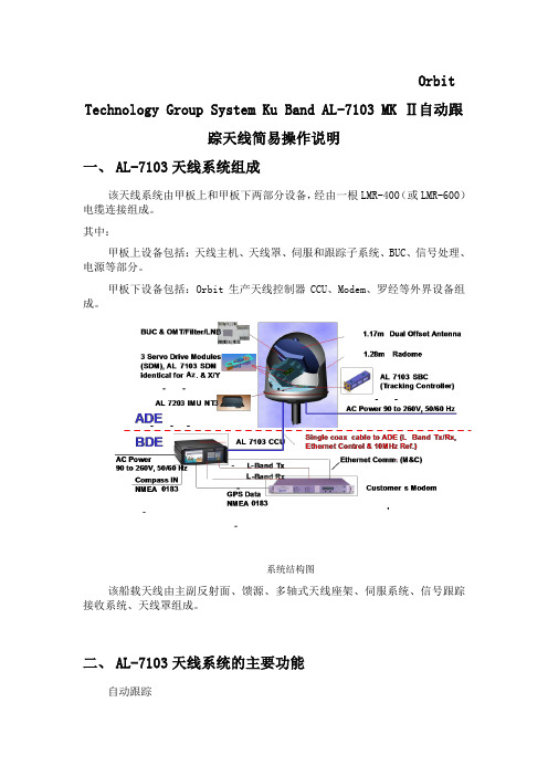
Orbit Technology Group System Ku Band AL-7103 MK Ⅱ自动跟踪天线简易操作说明一、AL-7103天线系统组成该天线系统由甲板上和甲板下两部分设备,经由一根LMR-400(或LMR-600)电缆连接组成。
其中:甲板上设备包括:天线主机、天线罩、伺服和跟踪子系统、BUC、信号处理、电源等部分。
甲板下设备包括:Orbit生产天线控制器CCU、Modem、罗经等外界设备组成。
系统结构图该船载天线由主副反射面、馈源、多轴式天线座架、伺服系统、信号跟踪接收系统、天线罩组成。
二、AL-7103天线系统的主要功能自动跟踪-在船体进行摇摆环境下,天线能够高精度跟踪地球同步卫星,保证通信系统进行高质量的通信。
自动捕星-控制、伺服系统通过采集航向信号、GPS数据,可对卫星进行自动搜索对准,进入自动跟踪状态。
位置预置及数据库-给控制计算机输入天线指向位置后,依托机内数据库,天线自动转到指定位置。
遮挡保护-当天线被遮挡,信号中断跟踪无效时,伺服系统自动报警并进入保护状态,信号恢复后,天线进入自动跟踪。
状态显示-实时显示天线的各轴角状态、航向、经纬度、跟踪等状态参数、告警及故障提示。
-模拟频谱分析,便于分析卫星信号。
三、AL-7103 MKⅡ简易图文操作说明完整的开关机及搜索卫星步骤加电开机,进入Windows CE操作系统后会自动加载MtsLink软件,版本号为Version 4.51,读取SBC数据下载进度条后进入软件主界面,此时会有IMU 计算船体横摇纵摇经纬度等参数计算,时间为360秒,时间到后IMU成锁定状态,如图:Screen,如图Coordinates选项框中为当前系统的日期、时间、经纬度以及船体横摇、纵摇参数和罗经船首向;AZ/EL Deviation选项框为天线指向卫星的目标;System Status选项框为当前系统使用的模式、IMU状态、极化选档度数和线极化的极化方式,极化的更改按Commands中的Polarization进行水平和垂直的更换;AGC(dbm)选项框直方图粉红色柱状条代表当前接收卫星载波的自动增益,绿色柱状条为当前选用的AGC参考门限;Satellite and Channel Select选项框为当前选择系统使用的卫星和信道,图中为110.5E鑫诺一号卫星;Antenna Position选项框为当前实际对准卫星后实时变化的方位角、俯仰角、极化角参数;Antenna Target选项框为在当前经纬度下对准所选用的卫星计算出来的标准方位角、俯仰角以及极化角的参数;Local Position选项框为天线ODU相对于本船本地化为参照物的方位角和俯仰角的参数;System Messages为系统运行信息,任何天线信息(绿色)、运转错误(蓝色)、故障告警(红色)会以代码及文字的方式显示在这个框中,并记录到CCU 中的Log。
ZTT-100天线调谐器说明书
一.概述ZTT-100型自动天线调谐器,是高频调谐器,其调谐频率范围为1.8-30MHZ(接12米天线时)。
是自动的数字控制调谐器。
内部使用了一个8位单片微计算机(8749)。
它可以从260000个不同的LC组合中,自动选出一个最佳的组合,以选择一个最小的驻波比(SWR),从而使电台在发射功率时,通过天调自动调谐,达到与天线阻抗匹配的目的。
ZTT-100型自动天线调谐器可以直接和IC-725电台相匹配,从而省去了人工调机的麻烦。
二.使用注意事项1.使用ZTT-100天调时,操作之前,必须将天线于天线端子接好,将地线于地线端子接好。
2.天线应安装在人们不易触摸到的地方,发射和调机时,天线上有高压,危险。
3.天线的长度应避免为使用频率的半波长或半波长的整倍数。
计算公式:天线长度不等于(K/2)入(M)。
K为正整数。
(1/2)入=150/f (使用频率:MHZ)(M)。
三.电缆连接高频电缆连接到IC-725后面板ANT插座上。
控制电缆连接到IC-725后面板TUNER插座上。
四.操作方法1.当IC-725电台刚开机或改变工作频率时,必须按前面板上的【TUNER】开关,以使调机。
2.接通无线电收发信机,按动【TUNER】开关时,无线电收发信机自动改变模式转到CW和发送低功率,电台液晶显示器上“TUNER”闪烁,说明天调正在调机,这时不可以发射功率或改变工作频率与方式。
3.当调谐完成后,“TUNER”稳定在电台液晶显示器上,说明调机成功,可以发射功率。
调谐最长需要20s,一般2-3s,最短1s.4.当调谐之后,电台液晶显示器上出现“THRU”说明调谐失败,不可以发射功率。
这时应检查天线连接及天线长度。
所接天线长度是使用频率的半波长或半波长倍数时,天调不能调谐,应避开该频率。
五.主要性能指标1.频率范围1.8-30MHZ (天线长度>=12米时3.5-30MHZ (使用AH-2B 3米鞭状天线时)2、最大输入功率120W3、输入阻抗50欧4、调机功率5-15W(调机时辐射功率小于0.3W)5、电压驻波比,小于或等于1.5:1 (天线长度为半波长或半波长倍数除外)6、平均调机时间:小于2.5s7、电源电压:DC+13.8V+-15%8、工作环境温度-10~+609、重量2.4kg10、外形尺寸(不包括=边接线柱)380mm 230mm 85mm。
MS27D使用说明

MS27D使用说明一、主要功能1.频谱分析:通过频谱分析功能,用户可以快速检测无线信号的带宽、占用频率、信号强度等参数。
2.信号监测:该设备可以实时监测并显示信号的频率、功率、调制方式、调制深度等信息。
3.调谐功能:通过调谐功能,用户可以快速找到想要监测的无线信号。
4.频谱保护:设备自带频谱保护功能,可以预先设置频谱范围,超出范围时会发出警报提醒。
5.数据存储:支持将测试结果通过USB接口存储到U盘或电脑中,方便后续数据分析和报告编制。
二、硬件说明1.屏幕显示:设备配备了一块大屏幕LCD显示屏,能够清晰显示各项参数和曲线图。
2.扫描控制:设备上配有扫描控制按钮,用户可以通过按钮进行频谱扫描和调谐操作。
3.天线接口:设备天线接口可连接各类天线,天线通过提高接收信号的灵敏度来获取更准确的测试结果。
4.电源适配器口:可连接外部电源适配器进行充电和供电。
三、操作步骤1.开机及设置a.按下电源键开机,待设备启动完成后,进入主界面。
b.在主界面上,通过旋钮选择所需功能,并按下确认键。
c.根据实际需求,在菜单中选择并设置相关参数,如频率范围、中心频率、RBW等。
2.扫描操作a.在主界面上选择“扫描”功能,并按下确认键。
b.设备开始扫描无线信号,并将结果显示在屏幕上。
c.可通过旋钮调整扫描速度,以及移动光标进行细致观察。
3.调谐操作a.在主界面上选择“调谐”功能,并按下确认键。
b.可通过频率、功率等参数找出要监测的无线信号。
c.调谐到目标信号后,可通过旋钮选择“监测”功能,并按下确认键。
4.数据存储与导出a.连接U盘或电脑,并确保设备与U盘或电脑连接正常。
b.在主界面上选择“数据存储”功能,并按下确认键。
c.选择数据存储的路径和格式,点击“保存”即可完成数据存储。
d.可通过USB接口将存储的数据导出到电脑进行分析和编制报告。
四、常见故障排除1.设备无法开机a.确保设备已充电或连接外部电源适配器。
b.检查电源是否插紧,或更换电源适配器。
天调使用说明
天调使用说明天调使用说明工作频段:40m波段、30 m波段、20 m波段、17 m波段、15 m波段、12m波段、10m波段驻波比:优于1.5:1(视天线阻抗范围)配接使用天线类型:非平衡式非平衡式天线接口:SL16型插座“TX”接口形式:SL16型插座(50 Ω)“TX”接口类型:非平衡式匹配天线阻抗范围:12 ~ 200 Ω(实际约:8 ~ 300 Ω)承载射频功率:不大于150W调谐所需射频功率:不小于2W功率测量范围:不大于200W驻波比测量范围:1 ~ 无穷大整机重量: 2.3Kg本“手动天调”集:功率驻波比表、天线调谐器于一体,无需另配价格昂贵的“驻波比表”,利用本手动天调自带的驻波比检测功能,使得调谐过程清晰明了,驻波比大小、功率大小、天线工作状态一目了然。
当选择不接入天调,直通时线调谐器部分不工作。
利用此功能,可对天调未接入前,以及天调已接入后,进行明确的对比性检测,以此来判断本“手动天调”的作用以及当前所使用天线的性能。
进行调谐前应将电台置于“CW”模式,将电台的发射功率调整至较小(3W左右)位置,调谐基本准确后(反射功率、驻波比较小)再逐渐加大发射功率进行精确调谐,否则若驻波比偏大、发射机给出的发射功率又较大时,将有可能造成发射机的损坏。
任何天调的阻抗匹范围都是有限的,若超出这一范围值时,将不能进行良好的匹配。
快速粗调简易操作方法确认“天调”与天线以及电台之间的连接可靠。
将电台的工作模式置为“CW”方式,将电台的发射功率调至约2-3W左右,按下电台的发射键,监看驻波比表上的反射功率值,旋转“调感”波段开关,找到反射功率最小的某一档位(此档位即可定为基本谐振点使用),分别调整“调容一”、“调容二”,继续观察表盘上的读数,将反射功率调至最小,此过程可能要往返多次,确认反射功率调至最小后,逐渐加大电台的发射功率至希望使用的发射功率大小后,再进行精细调整。
将驻波比调整到小于1:2以下时,将电台工作的模式调整至希望工作的模式后即可开始通联。
电子天线使用说明书

电子天线使用说明书一、产品概述电子天线是一种用于接收和发射电磁信号的设备,用于接收和传输无线电、电视、卫星和无线通信等信号。
本使用说明书旨在帮助用户正确使用电子天线,以达到最佳的信号接收效果。
二、产品组成1. 主体:由天线罩、电路板和连接线组成;2. 天线罩:用以保护并增强天线的接收和传输性能;3. 电路板:包含天线信号处理电路和连接接口。
三、使用步骤1. 连接电源:将电源线插入电源插座,并将电源插头插入电子天线的电源接口;2. 连接信号源:根据需要,选择相应的接口连接电视、电台或其它设备,确保连接稳定;3. 调整天线的方向:将电子天线放置在合适的位置,确保天线罩朝向信号源的方向;4. 搜索信号:在电视或设备的菜单中,选择自动搜索信号功能,等待搜索完成;5. 完成设置:根据信号搜索结果,完善设备的信号设置,并根据需要进行调整。
四、注意事项1. 安装位置:电子天线最好放置在接收信号最佳的位置,避免阻挡或干扰天线的信号接收;2. 稳定连接:使用连接线时请确保插头插紧,连接稳定,避免信号中断或质量下降;3. 室内使用:电子天线主要用于室内使用,如果需要室外使用,请确保防水措施;4. 信号调整:如果信号接收不理想,可以尝试调整天线的位置或方向,或使用信号放大器进行增强;5. 保养维护:请定期清洁电子天线,保持天线罩的干净,以提高信号接收效果。
五、故障排除1. 无信号:请检查信号源是否正常工作,确认连接线是否插紧,信号接口是否正确;2. 信号质量差:请检查天线的位置和方向,尝试调整天线的角度或位置,或使用信号放大器;3. 无法搜索到信号:请检查设备的信号设置是否正确,或尝试重新搜索信号。
六、免责声明1. 本产品仅适用于合法的无线电接收和传输应用,禁止用于非法用途;2. 用户在使用本产品时需遵守当地的无线电法规和相关规定;3. 由于用户的不当使用或违规操作所引起的问题和责任,本公司概不负责;4. 如有任何疑问或问题,请联系售后服务部门。
MASTR II 辅助接收器与天线匹配单元说明书

LBI-30766LMobile CommunicationsMASTR® IIAUXILIARY RECEIVER19D417546G7 & G8& ANTENNA MA TCHINGUNITS19C321150G1-G2Printed in U.S.A Maintenance ManualCopyright© 1978, General Electric CompanyLBI-307661DESCRIPTIONThe MASTR® II Station Auxiliary Receivers are available for mounting in MASTR II Base Stations or in MASTR II Multiple Receiver Stations. The Auxiliary Receiver consists of a 2-rack unit shelf with space for the receiver RF circuits, the oscillator/multiplier, the IFAS and MIF assemblies together with a System Board and a 10-V olt Regulator Board. 13 VDC is required to power the shelf.In MASTR II Base Station applications (Options 9538-9541), power for operating the Auxiliary Receiver is provided by the Base Station Power Supply. These options also include a 19B226307 Overlay Harness. Refer to the Interconnection Dia-gram listed in the Table of Contents.In MASTR II Multiple Receiver Station applications,power for operating the receivers is provided by a power sup-ply designed specifically for this station. Refer to LBI-30731.Operating an auxiliary receiver in voting systems where no external power supply is available requires the use of the 19C31 1855G1 Power Supply. This supply is mounted on the rear panel of the receiver. No service speaker should be used with this supply.The Auxiliary Receiver can be supplied with an Antenna Matching Unit (Options 9536 or 9537). A phone connector is used for interconnecting the receiver and AMU. When the re-ceiver is not used with an AMU, a coaxial cable (19A129312G4) fitted with an auxiliary UHF antenna connec-tor is provided. Refer to the Installation Instructions listed in the Table of Contents.The Auxiliary Receiver System Board accommodates sev-eral option boards either individually or in combination. Op-tion boards that plug into jacks on the System board include the V oting Tone Board (19C320880G1) used in Receiver V ot-ing Systems or the Squelch Operated Relay (SOR)19C320913G1, used in external control applications.A Secur-it Tone Notch Filter (19C328328G3), used in Tone Remote Systems, mounts on the side of the receiver system board chassis. A Line Response Compensator Board (19C328328G2) is available for use in V oting Tone Systems.This compensator provides means for adjusting the audio re-sponse at the receiver end of a telephone line. A third version of this board (19C328328G1) includes both the tone notch fil-ter and the line response compensator.A Channel Guard Decode Board (19D417261G6) may be plugged into the System Board at P908 and P909. A Tone Re-ject Filter (19C320627G1) is used with the Channel Guard De-code Board to prevent the CG tone from being fed into the telephone line. The filter attenuates below 203.5 Hertz.The 13-V olt DC input to the 10-V olt regulator is fused. A Light Emitting Diode (LED) is provided on the front panel of the receiver to indicate when power is applied. A power ON-OFF switch is provided on the regulator board. Another LED on the front panel indicates carrier activity. The receiver chas-sis swings out for servicing.INSTALLATIONThe Auxiliary Receiver is installed directly above the sta-tion power supply in MASTR II Base Stations. The 19C321150 Antenna Matching Unit is located directly above the Receiver. Refer to the Installation Diagram (See Table of Contents). Refer to the Installation Instructions in LBI-30761for mounting the Auxiliary Receiver in the Multiple Receiver Station.ADJUSTMENTThe initial adjustment for the receiver includes tuning the input circuit to match the antenna. Refer to the FRONT END ALIGNMENT PROCEDURE IN THE MAINTENANCE MANUAL for the receiver.MASTR II REMOTE CONTROL STATION ADJUSTMENTTo adjust the LINE LEVEL control R936, located on the System Board, use the following procedure.1.Connect a signal generator to the Auxiliary Receiverantenna jack J2402. Set the generator to the receiver frequency. Modulated at 3 kHz deviation by a 1000 Hz signal. Disable Channel Guard (if present) by opening switch S802 on the Regulator Board.2.Adjust the LINE LEVEL control R936 on the SystemBoard for a reading of 2.7-volts rms (+11 dBm) as measured at the base station audio pair.If the receiver is used with a Tone Control Base Station,adjust the LINE LEVEL control for a reading of 1.0-volt rms (+2 dBm).To adjust the VOL SET control R930 and the SQUELCH control R2401, use the following procedure.1. Connect an 8.2 ohm, l-watt resistor across J2401-9 and10, located on the rear panel of the Auxiliary Receiver.2. Connect an AC vtvm across the 8.2 ohm resistor andadjust R930 for a reading of 2.7-volts rms on the meter.3. Disconnect the 8.2 ohm resistor. Disconnect the signalgenerator.COMBINATION NOMENCLATURELBI-3076624. Turn the SQUELCH control R2401 clockwise (to theright) as far as possible.5. Adjust the VOLUME control R3 on the 19C320728service speaker until the noise is easily heard in thespeaker but is not annoyingly loud.6. Turn the SQUELCH control counter-clockwise (to theleft) until the noise just disappears, then advance thecontrol another 20 degrees.MASTR II LOCAL CONTROL BASE STATIONSTo adjust the VOL SET control R930 and the SQUELCH control R2401, use the following procedure.1. Apply a 1000 microvolt on-frequency signal modulatedby 1,000 Hz with ±3 kHz deviation to the Auxiliary Re-ceiver Antenna Jack J2402.2. Disconnect MASTR Local Controller cable from sta-tion input (PI 102 from J1).3. Connect an 8.0 ohm, 5-watt resistor across J2401-9 and10, located at the rear of the Auxiliary Receiver.4. Connect an AC vtvm across the 8.0 ohm resistor andadjust R930 for a reading of 6.3-volts rms on the meter.5. Disconnect the 8.0 ohm resistor and connect the con-troller cable to the station. Disconnect the signal gener-ator from J2402.6. Turn the SQUELCH control (R2401) clockwise (to theright) as far as possible.7. Adjust the VOLUME control on the MASTR LocalController until the noise is easily heard in the control-ler speaker but is not annoyingly loud.8. Turn the SQUELCH control counter-clockwise (to theleft) until the noise just disappears, then advance thecontrol another 20 degrees.LINE COMPENSATOR ADJUSTMENT,R12, R19Test Equipment Required1. Signal Generator2. Audio Oscillator3. AC V oltmeterProcedureR12 in the line compensator is used to set the 3000 Hzlevel. R19 is used to set the 300 Hz level. A Test Set-up Dia-gram is shown in Figure 1.1. At the Satellite Receiver, apply a 1000 millivolt, 1 kHzsignal with 3 kHz deviation from the signal generatorto the receiver as shown in Figure 1. Adjust LINEOUTPUT potentiometer R936 on Auxiliary ReceiverSystem Board for a reading of 0 dBm.2. Record this level as measured at telephone line input ofthe voting selector, then remove the signal generator.3. Connect the audio oscillator to the input of the linecompensator (Hole 14 on the Line Compensator Boardor J908 on the Auxiliary Receiver System Board). Setthe oscillator frequency to 1000 Hz, and adjust the levelto produce the same level recorded at the voting selec-tor input in Step 2.4. Record the output level of oscillator.5. Change the oscillator frequency to 2800 Hz. Maintainsame oscillator output level as recorded in Step 4.6. Adjust R12 on the line Compensator Board to producethe same level recorded at the voting selector in Step 2.7. Change the oscillator frequency to 300 Hz. Maintainsame oscillator level as recorded in Step 4.8. Adjust R19 on line compensator to produce the samephone line level at the voting selector as recorded inStep 2.CIRCUIT ANALYSIS10-VOLT REGULATOR BOARD19C320918G1The hybrid integrated circuit U801 includes the 10-V oltRegulator and regulator amplifier. Regulator pass transistorQ801 is mounted to the heat sink located on the printed board.The regulator circuit provides a closely controlled supply volt-age for the receiver, Channel Guard and other options whenpresent. Input voltage (A+) for the regulator is supplied fromthe station power supply via J2401-2 or some other externalsource.The Auxiliary Receiver ON/OFF switch S801 (located onthe Regulator Board) is normally left in the ON position. Turn-ing on the station power supply applies voltage throughS801 and input filter C801-L801 to pin 1 of the regulator hy-brid U801. The regulator amplifier output at pin 2 of U801 isapplied to the base of Q801, causing Q801 to conduct. Thevoltage at pin 3 of U801 is the regulated 10-volts output. Ahigh impedance source at pin 5 of U801 provides a stable 5-volt compensation input to the receiver ICOM.Two LEDs are provided on the front panel of the Re-ceiver. LED CR801 (ON) indicator is illuminated whenpower is applied to the regulator and switch S801 is in theON position. When a signal is received, the received un-squelch sensor (RUS) voltage developed by the receiver op-erates the RUS switch Q909 on the System Board.Conduction of Q909 operates Q802 on the regulator board.Conduction of Q802 turns on LED CR802 (CARRIER AC-TIVITY light).SYSTEM BOARD 19D429764G1The Auxiliary Receiver System Board contains the VOLSET control R930, the de-emphasis and line driver circuitsfor remote control applications, and jacks which accommo-date the various options available. The System Board alsomates directly with the receiver modules through J903 andJ904.VOLUME/SQUELCH HI from the receiver audio pre-amp is connected via J904-11 to the VOL SET control R930and SQUELCH control R2401. The VOL SET arm is re-turned to the receiver IFAS Board where the audio is ampli-fied by the receiver audio power amplifier circuit. The audiooutput of the PA is then connected to the speaker leads atJ2401-9 and 10. The station VOL SET control is normallyadjusted for 5-watts output and the speaker level is control-led by the MASTR Local Controller VOLUME control. Inmultiple-receiver applications, the jumper between H1 andH2 on the 19C320918 regulator board is removed, discon-necting A+ from the receiver PA output transformer. This al-lows the audio to be applied to the Multiple Receiver PA andspeaker and limits the current drain requirements.In MASTR II remote applications, the VOL/SQ HI iscoupled through the LINE DRIVER circuits to the remoteaudio pair. The audio is connected through the high-pass fil-ter consisting of C907-C908 and R901-R902. This filter at-tenuates 60 and 120 Hertz to reduce the hum and noise. Theoutput of emitter-follower Q901 is passed through a de-em-phasis network C909 and R906. This network provides a 6dB/octave rolloff. The signal is then amplified by Q902 andfed to another emitter follower Q903.The audio is coupled to the line driver through C914,Q904 amplifies the signal. The LINE LEVEL control R936is connected in the collector circuit of Q904 and allows feed-ing the audio to the line driver Q907. Q906 serves as anaudio switch controlled by the RUS circuit. As long as theRUS switch Q909 is turned off (receiver squelched), CR905is forward biased allowing Q906 to conduct. Conduction ofQ906 grounds the audio path between Q904 and Q907, pre-venting the audio from being passed to the line. When the re-ceiver unsquelches, the RUS lead goes high. This turns Q909on, turning off CR905 and Q906. The audio is now allowedto pass to the output amplifier Q908 or to the line trans-former T901. CR902, CR903 and VR901 are provided forline-surge protection.When the 19D417261G6 Channel Guard Board is used,the RX MUTE lead is controlled by the Channel GuardBoard. When no CG tone of the proper frequency is present,the board holds the RX MUTE lead at ground potential.When a CG tone of the proper frequency is detected, theground on the RX MUTE lead is removed and the RUS leadwill then go high when the receiver squelch opens. Activat-ing the CG MONITOR switch at the station control unitcauses the Channel Guard Board to remove ground from theRX MUTE lead, allowing the receiver to operate on noisesquelch.Figure 1 - Test Set-up DiagramLBI-307663CHANNEL GUARD FILTER 19C320627G1 The Channel Guard filter attenuates frequencies below 203.5 Hz to prevent the Channel Guard tone from being ap-plied to the line. The filter board is plugged into the System Board at P906 and P907.Audio and tone is applied to the filter input (J1-1) from the pre-amp. The audio is coupled to the 187 Hz notch filter composed of Q1, Q2 and associated circuitry. Negative feed-back for the filter is connected from the collector of Q2 to the junction of C2-R2.The notch filter output is applied to a low-pass filter con-sisting of Q3 and Q4. Negative feedback is developed across R12. The output of Q4 is coupled to the output lead J2-3 through C9 and returned to the preamp circuit.TONE NOTCH FILTER 19C328328G3 In Tone Remote Systems the tone notch filter is used for removing the 2175 Hz Secur-it tone from the audio path. The audio is connected to the filter at J906 on the System Board. The filter is composed of series resonant shunts L1-C1 and L3-C3 along with parallel resonant trap L2-C2. The filter notches out the 2175 Hz component from the audio and returns the audio to the System Board via J905. Resistor R937 is removed in Tone Remote Systems.LINE RESPONSE COMPENSATOR19C328328G2A telephone line usually introduces attenuation as a func-tion of frequency to the audio signal. The line response com-pensator introduces gain at the appropriate frequencies with the net effect being a flat frequency response.Audio applied to the compensator input at J908 on the System Board is amplified by buffer amplifier AR1-D and applied to the two active bandpass filters AR1-A and AR1-B. The 300 Hz and 3000 Hz filters boost the audio at these fre-quencies and the result is summed by the low-Q 1000 Hz fil-ter AR1-C. This 1000 Hz filter provides the required attenu-ation for a resultant response control from -1 to +10dB at3000 Hz, 3000 Hz referenced to the 1000 Hz level. Gaincontrol R12 is adjusted at the factory and should require nofurther adjustment. The compensator output is applied toJ909 on the System Board. The +10 Vdc for operating thecompensator circuits is applied via J910 on the SystemBoard.TONE NOTCH FILTER/LINE RESPONSECOMPENSATOR 19C328328G1The 19C328328G1 board combines the tone notch filterand line response compensator in systems requiring bothfunctions.SQUELCH OPERATED RELA Y BOARD19C320913G1The Squelch Operated Relay (SOR) Board plugs into theAuxiliary Receiver System Board at the P902 position. TheSOR provides four set of Form "C" relay contacts. A harness(19A122717G5) is provided for connecting any two sets ofthe Form "C" contact pines. The contacts of the relay arerated at 2 Amperes, for either 24 VDC or 121 V AC applica-tion.When a signal is received and the receiver unsquelches, apositive voltage appears on the RUS line at P904-8. Thispositive voltage is applied to the base of Q1, turning thetransistor on. Conduction of Q1 operates Q2. Conduction ofQ2 turns on Q3 which, in turn, energizes relay K1.VOTING TONE BOARD 19C320880G1The V oting Tone Board is used in V oting Selector Sys-tems and is plugged into the same plug (P902) which accom-modates the SOR Board. Thus both of these options cannotbe used simultaneously. Refer to LBI-4913 for a descriptionof the V oting Tone Board.VOTING TONE BOARD 19C336900G1The V oting Tone Board is used to provide tone signalingand is plugged into the same plug (P902) which accommodatesthe SOR Board. Thus both options cannot be used simultane-ously. Refer to LBI-31981 for more information on this board.VOTING TONE BOARD 19C328276G2(Option 9656)The 19C328276G2 V oting Tone Board is used in V otingSystems when test tones are desired for line response adjust-ment. The test tones are normally 400, 1000 and 2500 Hz withoptional status tone of 1600, 2175 and 2400 Hz available.Three momentary pushbutton switches are provided for ena-bling each of the test tones. The 19C328276G2 V oting ToneBoard is described in LBI-30767.ANTENNA MATCHING UNITS(Options 9536-9537)The Antenna Matching Units (AMU) are designed to matchtwo or more (up to a total of four) receivers to a single antenna.The AMUs may be operated with any receiver having an inputimpedance of approximately 50 ohms. The AMU chassis is de-signed for standard rack mounting. The frequency range ofAntenna Matching Unit Options 9536 and 9537 are usedwith MASTR II Base Station Auxiliary Receiver applications.Options 9703 and 9704 are used with MASTR II Multiple Re-ceiver Stations.The receive antenna is connected to J1 on the AMU. Theantenna cable W1 is connected to the input jack J1 on the firstpower divider (Z1 or Z4). The two outputs of the first powerdivider (J2 and J3) are coupled to the input jacks of two otherpower dividers which, in turn, feed up to four receivers. Eachpower divider has a 3.5 dB loss and 20 dB isolation (15 dB inthe 450-512 MHz unit) between output posts. The charac-teristic impedance of all four receiver output posts on thepower dividers is 50 ohms to match the input impedance of thereceivers. If only two receivers are used with an AMU, the in-sertion loss can be reduced by 3.5 dB if only one power divideris used.POWER SUPPLY 19C311855G1The 19C311855G1 Power Supply is used when more thanone auxiliary receiver is used in the MASTR II station. The120-V olt, 50/60 Hz supply provides the required +13 V olts foroperating the receiver.Connecting P501 to a voltage source applies 120 V AC tothe primary of stepdown transformer T501. The AC voltage de-veloped across the secondary windings of T501 is rectified byfull-wave bridge rectifiers CR501 through CR504. The recti-fied output is filtered by C501 and regulated by VR501 andQ501. The +13 V output is connected through P502 and P503to P1-1 and P1-2 on the 19B226440G2 harness.LBI-30766 4LBI-30766 OUTLINE DIAGRAMAUXILIARY RECEIVER CHASSISLO-BAND, HI-BAND & UHF19D417546G75OUTLINE DIAGRAM LBI-30766800 MHz AUXILIARY RECEIVER CHASSIS19D417546G86OUTLINE DIAGRAMCHANNEL GUARD & TONE NOTCH FILTERS19C320627G1 19C328328G1-G3 (19C321338, Rev. 1)(19C320625, Sh. 2 , Rev. 1)CHANNEL GUARD FILTER 19C320627G1(19C328331, Rev. 0)(19B232614, Sh. 1, Rev. 0)TONE NOTCH FILTER/LINE RESPONSECOMPENSATOR 19C328328G1-G3LBI-307667OUTLINE DIAGRAMAUXILIARY RECEIVER SYSTEM BOARD 19D429764G1(19D429765, Rev. 2) (19B232874, Sh. 1, Rev. 2)AUXILIARY RECEIVER SYSTEM BOARD 19D429764G1 LBI-307668OUTLINE DIAGRAM(19C321796, Rev. 1)(19A130059, Sh. 1 & 2, Rev. 0)(19C321792, Rev. 4)(19B226221, Sh. 1 & 2, Rev. 1)AUXILIARY RECEIVER & 10-VOLT REGULATOR BOARDS19C320913G1 19C320918G1 AUXILIARY RECEIVER SOR BOARD 19C320913G110-VOLT REGULATOR 19C320918G1LBI-307669OUTLINE DIAGRAM ANTENNA MATCHING UNITS 19C321150G1 & G2ANTENNA MATCHING UNITS AND POWER SUPPLY 19C321150G1 & G2 19C311855G1 (19C321706, Rev. 0) (19C311855, Rev. 5)POWER SUPPLY 19C311855G1LBI-30766SCHEMATIC DIAGRAMCHANNEL GUARD FILTER AND POWER SUPPLY 19C320627G1 19C311855G1 (19C320628, Rev. 0)(19B216280, Rev. 5)TONE NOTCH FILTER19C328328G3(19C328343, Rev. 1)LBI-30766LBI-30766SCHEMATIC DIAGRAMLINE RESPONSE COMPENSATOR19C328328G1(19D429483, Rev. 1)LBI-30766 SCHEMATIC DIAGRAMLINE RESPONSE COMPENSATOR19C328328G2(19D429481, Rev. 2)SCHEMATIC DIAGRAMSQUELCH OPERATED RELAY 19C320913G1(19C320915, Rev. 3)ANTENNA MATCHING UNITS 19C321150G1 & G2(19B226529, Rev. 1)LBI-30766PARTS LIST LBI-30766PARTS LIST LBI-30766PARTS LIST LBI-30766PARTS LIST LBI-30766PARTS LIST LBI-30766PARTS LIST LBI-30766SCHEMATIC DIAGRAM AUXILIARY RECEIVER 19D417546G7 & G8(19E501751, Sh. 1, Rev. 9)NOTES:1. JUMPER FROM H1 TOTO H2 NOT PRESENTWHEN THERE IS NO LOAD,OR SPEAKER CONNECTEDTO THE SPEAKER OUTPUTLEADS. (J2401-9,10).2. WHEN TONE FILTERPL19C328328G1,3 IS PRE-SENT (IN TONE CONTROLSYSTEMS) R937 IS RE-MOVED.3.VOL SET CONTROL R930 ISSET FOR 1 W A TT AUDIOOUTPUT IN NON-LOCALSTA TIONS, 5 W A TTS IN LO-CAL STA TIONS.4.WHEN C.G. FILTER BD19C320627 IS NOT PRE-SENT, JUMPER FROM H20TO H21 IS PRESENT.5.WHEN AUX RECEIVERAUDIO IS RUN DOWNSEPARA TE 600Ω LINE, RE-MOVE JUMPERS FROM H2TO H22 AND H24 TO H25.6.ALL WIRES N22 UNLESSOTHERWISE NOTED.7.TERMINA TE N22 WIRES TOP2401 AND P2402 WITH19A116781P4. TERMINA TEV18 WIRES TO P2401 ANDP2402 WITH 19A116781P3.8.WHEN USED WITH MASTRII STA TION USING COM-MON TELEPHONE LINE,R931 IS NOT PRESENT.9.• 900 MHz ONLY .♦ LB. HB & 450 MHz.10.WHEN LINE COMPENSA-TOR PL19C328328G1,G2 ISPRESENT, DA JUMPER BE-TWEEN H34 AND H35 ISNOT PRESENT.11.v WIRES ADDED ANDRUNS CUT WHEN MODI-FIED FOR PST VOTING.12.5.6K RESISTOR ADDEDFROM J935-1 TO J935-3WHEN MODIFIED FOR PSTVOTING.LBI-30766LBI-30766INSTALLATION INSTRUCTIONSTONE NOTCH FILTER/LINE RESPONSE COMPENSATOR19C328328G1-G3(19D417634, Sh. 3, Rev. 0)LBI-30766 INSTALLATION INSTRUCTIONSAUXILIARY RECEIVER & ANTENNA MATCHING UNIT(19D417615, Sh. 1, Rev. 5)LBI-30766INSTALLATION INSTRUCTIONSAUXILIARY RECEIVER & ANTENNA MATCHING UNIT(19D417615, Sh. 2, Rev. 8)LBI-30766 INTERCONNECTION DIAGRAMAUXILIARY RECEIVER OVERLA Y HARNESS19B226307G1(19D417611, Sh. 1, Rev. 12)LBI-30766INTERCONNECTION DIAGRAMAUXILIARY RECEIVER OVERLAY HARNESS (EACOM)19B226307G2(19D424989, Rev. 3)LBI-30766INTERCONNECTION DIAGRAMWITH CHANNEL GUARD MONITOR。
M.2 GPS用户指南说明书
M.2 GPS CTIM-000454 Revision 0.01 2021-03-01TABLE OF CONTENTSTable of Contents (2)Preface (3)Disclaimer (3)Customer Support Overview (3)Contact Information (3)Limited Product Warranty (4)Copyright Notice (4)Trademark Acknowledgment (4)ESD Warning (5)Revision History (5)Introduction (6)Product Features and Specifications (6)Part Numbers / Ordering Information (6)Product Overview (7)Block Diagram (7)Connector Summary & Locations (7)Interface Pin-outs (8)M.2 Edge Connector (8)External I/O Connector (9)Active Antenna Connector (9)Detailed Feature Description (10)USB (10)TIMEPULSE (10)W_DISABLE1# (10)External Interrupt Input/WHEELTICK Input (10)FWD (11)External Battery (11)Local Battery and BAT_EN Header (11)On-Board Indicator LEDs (11)Software Support for the NEO-7 and NEO-M8 GPS Receivers (12)Cables (13)CBG162 – External I/O Cable (13)CBG214 – Murata HSC to SMA Female Cable (13)PREFACEDisclaimerThe information contained within this user’s guide, including but not limited to any product specification, is subject to change without notice.Connect Tech assumes no liability for any damages incurred directly or indirectly from any technical or typographical errors or omissions contained herein or for discrepancies between the product and the user’s guide.Customer Support OverviewIf you experience difficulties after reading the manual and/or using the product, contact the Connect Tech reseller from which you purchased the product. In most cases the reseller can help you with product installation and difficulties.In the event that the reseller is unable to resolve your problem, our highly qualified support staff can assist you. Our support section is available 24 hours a day, 7 days a week on our website at: https:///support/resource-center/. See the contact information section below for more information on how to contact us directly. Our technical support is always free.Contact InformationContact InformationMail/Courier Connect Tech Inc.Technical Support42 Arrow RoadGuelph, OntarioCanada N1K 1S6Contact Information ********************************************Toll Free: 800-426-8979 (North America only)Telephone: +1-519-836-1291Facsimile: 519-836-4878 (on-line 24 hours)Support Please go to the Connect Tech Resource Center for product manuals,installation guides, device drivers, BSPs and technical tips.Submit your technical support questions to our support engineers.Technical Support representatives are available Monday through Friday,from 8:30 a.m. to 5:00 p.m. Eastern Standard Time.Limited Product WarrantyConnect Tech Inc. provides a 2-year Warranty for this product. Should this product, in Connect Tech Inc.'s opinion, fail to be in good working order during the warranty period, Connect Tech Inc. will, at its option, repair or replace this product at no charge, provided that the product has not been subjected to abuse, misuse, accident, disaster or non-Connect Tech Inc. authorized modification or repair.You may obtain warranty service by delivering this product to an authorized Connect Tech Inc. business partner or to Connect Tech Inc. along with proof of purchase. Product returned to Connect Tech Inc. must be pre-authorized by Connect Tech Inc. with an RMA (Return Material Authorization) number marked on the outside of the package and sent prepaid, insured and packaged for safe shipment. Connect Tech Inc. will return this product by prepaid ground shipment service.The Connect Tech Inc. Limited Warranty is only valid over the serviceable life of the product. This is defined as the period during which all components are available. Should the product prove to be irreparable, Connect Tech Inc. reserves the right to substitute an equivalent product if available or to retract the Warranty if no replacement is available.The above warranty is the only warranty authorized by Connect Tech Inc. Under no circumstances will Connect Tech Inc. be liable in any way for any damages, including any lost profits, lost savings or other incidental or consequential damages arising out of the use of, or inability to use, such product.Copyright NoticeThe information contained in this document is subject to change without notice. Connect Tech Inc. shall not be liable for errors contained herein or for incidental consequential damages in connection with the furnishing, performance, or use of this material. This document contains proprietary information that is protected by copyright. All rights are reserved. No part of this document may be photocopied, reproduced, or translated to another language without the prior written consent of Connect Tech, Inc.Copyright 2021 by Connect Tech, Inc.Trademark AcknowledgmentConnect Tech, Inc. acknowledges all trademarks, registered trademarks and/or copyrights referred to in this document as the property of their respective owners. Not listing all possible trademarks or copyright acknowledgments does not constitute a lack of acknowledgment to the rightful owners of the trademarks and copyrights mentioned in this document.ESD WarningElectronic components and circuits are sensitive to ElectroStatic Discharge (ESD). When handling any circuit board assemblies including Connect Tech COM Express carrier assemblies, it is recommended that ESD safety precautions be observed. ESD safe best practices include, but are not limited to:• Leaving circuit boards in their antistaticpackaging until they are ready to be installed. • Using a grounded wrist strap when handlingcircuit boards, at a minimum you should touch a grounded metal object to dissipate any static charge that may be present on you.• Only handling circuit boards in ESD safe areas,which may include ESD floor and table mats, wrist strap stations and ESD safe lab coats. • Avoiding handling circuit boards in carpetedareas.• Try to handle the board by the edges, avoidingcontact with components.REVISION HISTORYRevisionDateChanges0.00 2016-03-18 Initial Release0.01 2021-03-01 Updated formatReplaced GPS-06T PN /w MSG095INTRODUCTIONConnect Tech’s M.2 GPS is a GNSS receiver based on the very small industry standard M.2 Type-2242-S3-B form factor. Using the USB bus, the M.2 GPS provides global positioning and time-stamp information, while taking up little space and power within a system. Also considering the existing support for Windows and Linux, the M.2 GPS can be easily integrated into any existing system, as well as easily implemented into new systems.Product Features and SpecificationsSpecificationsDimensions 42 mm x 22 mm (M.2 Type-2242-S3-B)Antenna Connector HSC (MHF4), support for active antennas onlyGPS GPS, GLONASS, QZSS, GalileoUBX, RTCM, NMEA protocolsI/O TIMPULSE output synchronized with GPS time gridWHEELTICK input (used for Automotive Dead Reckoning)FWD input (used for Automotive Dead Reckoning)External Interrupt InputExternal Battery InputCables CBG162: External I/O CableCBG214: HSC (MHF4) to SMA Female CableAntenna MSG095, VTGPSA-9, Active GPS/GLONASS antennas only Environmental -40ºC to +85ºCWarranty and Support 2 YearsPart Numbers / Ordering InformationPart NumberM2G201 M.2 GPS Receiver (Battery not included) populated with NEO-7N moduleM2G202 M.2 GPS Receiver (Battery included) populated with NEO-7N moduleM2G203 M.2 GPS Receiver (Battery not included) populated with NEO-M8N module M2G204 M.2 GPS Receiver (Battery included) populated with NEO-M8N moduleM2G205 M.2 GPS Receiver (Battery not included) populated with NEO-M8L module,supports Automotive Dead ReckoningM2G206 M.2 GPS Receiver (Battery included) populated with NEO-M8L module,supports Automotive Dead ReckoningPRODUCT OVERVIEW Block DiagramConnector Summary & LocationsInterface Pin-outsM.2 Edge ConnectorThe M.2 GPS pin-out is compliant to the M.2 Socket 2 with B Key. This module uses only +3.3V for input power and all I/O is +3.3V signaling.Function M.2 Card Edge ConnectorLocation P3Pinout Signal Pin Pin SignalNC 1 2 +3.3V GND 3 4 +3.3V GND 5 6 NC USB_D+ 7 8 W_DISABLE1#USB_D- 9 10 NC GND1112 Connector Key Connector Key 13 14 Connector Key Connector Key 15 16 Connector Key Connector Key 17 18 Connector KeyConnector Key 19 20 NC CONFIG_0(GND)21 22 NC NC 23 24 NC NC 25 26 NC GND 27 28 NC NC 29 30 NC NC 31 32 NC GND 33 34 NC NC 35 36 NC NC 37 38 NC GND 39 40 M.2 GNSS SCL NC 41 42 M.2 GNSS SDA NC 43 44 M.2 GNSS IRQGND 45 46 NC NC 47 48 NC NC 49 50 RESET# GND5152NCNC 53 54 NC NC 55 56 NC GND 57 58 NC NC 59 60 NC NC 61 62 NC NC 63 64 NC NC 65 66 NC NC 67 68 NC CONFIG_1 (GND) 69 70 +3.3V GND7172+3.3VExternal I/O ConnectorThe pinout for the I/O connector is outlined in the table below.Function External I/O Connector501568-0507LocationP2Connector PN 501568-0507 - Manufacturer: Molex Mating Connector PN 501330-0500 - Manufacturer: Molex CTI Cable #: CBG162 PinoutPin SignalDescription1 EXT_INT / WHEELTICK External Interrupt Input orSpeed pulse input 2 TIMEPULSE Time pulse Output 3 FWD Forward/Reverse indicator 4 GND Digital Ground 5 EXT_BATExternal Battery InputNOTE: WHEELTICK is only available on M2G205 and M2G206, otherwise this signal is EXT_INTNOTE: FWD is only available on M2G205 and M2G206, otherwise it is not connected and should be left floatingActive Antenna ConnectorFunction Active Antenna ConnectorHSC - MHF4 JackLocation J2Connector PNMM4829-2702RA4 - Manufacturer: MurataMating Connector PN HSC – MHF4 Socket Standard CTI Cable #: CBG214DETAILED FEATURE DESCRIPTIONUSBThe M.2 GPS uses a USB 2.0 Full Speed (12Mb/s) interface as the primary communication bus. The USB interfaces is connected between the GPS receiver and the M.2 card edge connector (pins 7/9).TIMEPULSEThe TIMEPULSE output is a buffered and ESD protected signal from the GPS receiver. This signal connects to pin 2 of the External I/O Connector. It also drives the TIMEPULSE LED. By default, when satellites are not fixed this signal is High (3.3V). When satellites are fixed, this signal pulses at 1 pulse-per-second (1Hz) with a 20% duty cycle (200ms High, 800ms Low). For more information see the Receiver Description Including Protocol Specification document for your GPS receiver found in the Software Support section of this document.W_DISABLE1#The W_DISABLE# input from the M.2 card edge connector (pin 8) can be used to enable and disable power to the M.2 GPS module. When W_DISABLE1# is low, the module is disabled and no power is applied to the M.2 GPS. When W_DISABLE1# is High, the module is enabled and powered on. This signal is locally pulled up to 3.3V through a 100K ohm resistor.External Interrupt Input/WHEELTICK InputThe external interrupt/WHEELTICK input is an ESD protected input signal from the external I/O connector to the GPS receiver. On modules that do not support Automotive Dead Reckoning, this signal will always be an External Interrupt input, and this input can be used for control of the GPS receiver or for aiding. On modules that support Automotive Dead Reckoning (M2G205/M2G206), this signal is by default used as the WHEELTICK input and is used to provide speed pulse information to the module. If the speed pulse information is available from the host processor, then the information can be provided using software messages in the UBX protocol. If using software messages to provide speed pulse information, this signal can be configured as an external interrupt input. See the Receiver Description Including Protocol Specification document for your GPS receiver found in the Software Support section of this document. If this signal is not used, it should be left floating. Do not exceed 3.6V on this signal.FWDThe forward/reverse signal is an ESD protected input used on modules that support Automotive Dead Reckoning. This signal is used to indicate the moving direction of the module. An active high indicates moving forward and a low for moving backwards. If the forward/reverse information is available from a host processor, then this information can be provided to the module using software messages in the UBX protocol. For more information see the Receiver Description Including Protocol Specification document for your GPS receiver found in the Software Support section of this document. On modules that do not support Automotive Dead Reckoning, this signal should be left floating. Do not exceed 3.6V on this signal.External BatteryThe external battery input in an ESD protected input from the External I/O Connector to the backup voltage supply of the GPS receiver. The purpose of a battery signal is to power internal memory for GPS almanac, ephemeris, and last position retention through power cycles. The voltage on this input signal should be greater than 2.0V and less than 3.6V. The supply of this signal should be able to provide at least 20uA continuous at room temperature, and 50uA at +85 degrees Celsius.Local Battery and BAT_EN HeaderThere is a local battery supply on the M.2 GPS. The purpose of a battery signal is to power internal memory for GPS almanac, ephemeris, and last position retention through power cycles. The design includes a MS621 rechargeable battery which recharges itself when the unit is powered on. When power is removed from the unit the GPS receiver will typically consumer 15uA on its battery supply input at room temperature and 24uA at 85 degrees Celsius.On-Board Indicator LEDsLED DescriptionTIMEPULSE TIMEPULSE visual indicator. This LED will blink at the rate and duty cycle of the TIMEPULSE output.PWR ON: indicates the module is powered on and enabledOFF: indicated the module is not powered and is disabled*the module is enabled/disabled using the W_DISABLE1# input from the M.2 card edge connectorSoftware Support for the NEO-7 and NEO-M8 GPS ReceiversThe USB drivers for the NEO-7 and NEO-M8 GPS Receivers can be found on the u-Blox website: https:///en/product-resources?f[0]=property_file_product_filter%3A2668&f[1]=field_file_category%3A221For configuration and setting options for the NEO-7 GPS receiver, please refer to the u-Blox 7 Receiver Description Including Protocol Specification V14 found on the u-Blox website:https:///en/product-resources?f[0]=field_file_category%3A209For configuration and setting options for the NEO-M8N GPS receiver, please refer to the u-Blox M8 Receiver Description Including Protocol Specification found on the u-Blox website:https:///en/product-resources?f[0]=field_file_category%3A209Changing the configuring of the NEO modules is best accomplished using the u-center application provided by u-Blox. To get the u-center application for windows, please see the link below: https:///en/product/u-center-windowsCABLESCBG162 – External I/O Cable501330-0500SignalOpen End (Un-terminated) 1See I/O Connector Section for pin-outUn-terminated 2 Un-terminated 3 Un-terminated 4 Un-terminated 5 Un-terminatedCBG214 – Murata HSC to SMA Female CableHSCTOSMA Female (Socket)。
天调套件说明书V2
手动天调套件说明书V2天调可以将原来不谐振的天线,通过加入适当的电感或电容,使电台能正常工作。
可以将原来是谐振的天线,但由于受外界的影响,使有了变化的天线的SWR加以修正。
可以作为带通滤波器,发射时可以减少不必要的带外辐射,接收时又可以减少带外的交叉调制和干扰。
本天调套件自带驻波指示、采用T型拓扑网络,工作在短波1-30MHz,可承受15W的发射功率,调谐范围约40-300欧,能非常方便的进行QRP通信,确保进行高效率的无线电收发通信,同时也能让您充分享受DIY的乐趣。
本套件包括原件如下:类别 名称 数量机壳 防水密封盒(孔已经打好) 1个 贴纸(需要自行裁剪) 1张 M座 2个 普通电线 1段 M3沉头螺钉 8个 M3螺母 8个 M3垫片(用于M头接地) 12个可变电容 可变电容 2个 小旋钮 2个 M2.5沉头螺钉(用于固定可变电容) 4个 M2.5圆头螺钉(用于固定可变电容的旋钮) 2个 M3平垫片 2个 M3 螺母 2个多刀开关 多刀开关(12个档位) 1个 大旋钮 1个 T106-2 磁环(红色) 1个 0.5 漆包线 1段电路板 电路板(驻波指示器) 1块 档位开关 1个 红色发光二极管 1个 51欧 电阻 3个 FT37-43 磁环(黑色) 1个 1K 电阻(用于发光二极管限流) 1个 1N60二极管 1个 0.1uF电容 1个一、原理图动手制作之前,请仔细查阅这张图。
1、电路图如下:二、制作过程1、制作之前,请准备好烙铁、焊锡丝、剪刀、小刀、万用表等工具。
并根据原件表核对原件。
2、去除外壳内部多余塑料柱,位于下图的下方,建意先使用斜口钳子将塑料柱去剪掉,再使用电烙铁将多余部分烫平(注意不要烫太长时间,防止将整个塑料烫化,影响正面效果)。
3、安装两个M头到机壳。
安装过程中需要注意6个垫片的位置,它们的作用是理好的接地连接。
4、裁剪贴纸,贴于壳上。
效果图如下:两侧文字部分需要裁剪:5、安装可变电容及旋钮到外壳。
FIBOCOM EVB-M2 用户指南说明书
FIBOCOM EVB-M2 用户指南文档版本:V1.0.3更新日期:2020-07-23适用型号序号产品型号说明1 FM150-NA NA2 FM150-AE NA3 L8系列NA版权声明版权所有©2020 深圳市广和通无线股份有限公司。
保留一切权利。
非经本公司书面许可,任何单位和个人不得擅自摘抄、复制本文档内容的部分或全部,并不得以任何形式传播。
注意由于产品版本升级或其他原因,本文档内容会不定期进行更新。
除非另有约定,本文档仅作为使用指导,本文档中的所有陈述、信息和建议不构成任何明示或暗示的担保。
商标申明为深圳市广和通无线股份有限公司的注册商标,由所有人拥有。
版本记录文档版本编写人主审人批准人更新日期说明V1.0.3 李升根刘汉章许绍锋2020-07-23 在第1.2节中,增加对开发套件盒中USB线的区别说明。
V1.0.2 李升根刘汉章许绍锋2020-06-22 1、文件名由用户使用手册改为用户指南。
2、修改一些符号与格式错误。
V1.0.1 李升根刘汉章许绍锋2020-03-25 增加第5章开发板与电脑连接V1.0.0 刘汉章许绍锋许绍锋2020-03-05 初始版本目录1EVB 简介 (5)1.1产品概述 (5)1.2产品外观 (5)1.3应用框架图 (8)2跳线配置 (9)2.1默认跳线配置 (9)2.2电源跳线配置 (9)2.3ON/OFF跳线配置 (11)2.4PCIe接口配置 (11)2.5LED 信号跳线 (12)2.6USB_CFG跳线配置 (12)3信号配置开关 (14)3.1mmW 模组功能配置开关 (14)3.2SIM2 接口开关设置 (14)3.3音频功能开关配置 (15)3.4SIM_DET信号配置 (16)4天线连接器 (17)5开发板与电脑连接 (18)5.1开发板通过USB与电脑连接 (18)5.2开发板通过PCIe与电脑连接 (19)1 EVB 简介1.1 产品概述EVB-M2 开发板(简称EVB)适用于Fibocom 4G / 5G M.2接口模块测试与评估开发。
Comet CAT-300天线调谐器说明书
QST April 2023 5Reviewed by Phil Salas, AD5X *************I suspect that one of the most com-mon accessories found in the ham shack is an antenna tuner. Andwhile autotuners have become quite popular, the manual antenna tuner fi lls the needs of many hams. The Comet CAT-300 antenna tuner is a rugged manual antenna tuner that handles power levels up to 300 W.Basic DescriptionLike most manual antenna tuners, the CAT-300 is a T -confi guration antenna tuner. This antenna tuner can handle up to 300 W PEP of RF from 160 through 6 meters. It includes a colorful 1.8 × 2.5-inch analog cross-needle meter that simultaneously displays for-ward, refl ected power, and SWR. There is a pair of high-voltage variable capacitors, and a tapped shunt inductor (actually, two series inductors). Controls in-clude a 30/300 W range selector, PEP and average power reading, a TUNER switch that bypasses the CAT-300 while leaving the power and SWR functions intact, an ANTENNA 1 or ANTENNA 2 switch, the normal transmit and antenna variable capacitor, and tapped inductor (BAND ) control. On the rear panel, you will fi nd three SO-239 connectors — one INPUT to connect your transceiver, and two outputs to connect your an-tennas (see Figure 2). Please note that there are two possibilities for the ANTENNA 2 output, using either the SO-239 or the WIRE ANT banana jack for a wire antenna. There is no internal balun. Figure 3 shows the internal view of the CAT-300, and the complete specifi cations are given in Table 2.The BAND switch selects the shunt inductor tap. This may or may not be associated with the listed band, depending on the mismatch. The CAT-300 two-sheet manual lists starting capacitor and inductor positions for a 50 Ω input and 50 Ω output. This was a good starting point for my adjustments, as I was gradually increasing the resistive mismatch. However, for real on-the-air SWR adjustments, I recommend the tech-nique described by Andrew S. Griffith, W4ULD, in “Getting the Most Out of Your T -Network AntennaComet CAT-300 1.8 – 50 MHz Manual Antenna TunerBottom LineFor those hams interested in a manualantenna tuner, the Comet CAT-300 is certainly worth considering. It should easily satisfy the needs of 100 – 200 W radios for most anyantenna system mismatches.Table 2Comet CAT-300Manufacturer’s Specifi cations (not tested by the ARRL Lab)Frequency range: 1.8 – 54 MHz Input impedance: 50 ΩOutput impedance: 10 – 600 ΩMaximum TX power: 300 W PEP Minimum SWR measurement power: 6 W Lighting power supply: 11 – 15 V dc at 250 mA maximum*Dimensions (width, height, depth): 9.8 × 3.9 × 9.5 inchesWeight: 6 pounds*The actual current was only about 20 mA. I suspect that the original CAT -300 used an incandescent lamp for meter illumination. When this was changed to LEDs, apparently the current spec was not revised.Figure 2 — The Comet CAT-300 rear panel.6 April 2023 QST Tuner” in the January 1995 issue of QST . This entails the following procedure:1. Start with both capacitors in their center (half-meshed) posi-tions.2. Switch the shunt inductor to fi nd maximum receiver noise.3. Transmit 5 – 10 W and rotate the output capacitor, looking for an SWR dip.4. If no dip is seen, switch the inductor up or down and try again.5. Once an SWR dip is found, adjust the input capacitor for best SWR.6. Rock the output capacitor, and vary the input capacitor, until you fi nd the lowest SWR.My matching tests are shown inTable 3. I found that the adjustments were very touchy on 20 meters and above. However, it was fairly easy to null the SWR using the analog meter on the CAT-300. The input SWR was measured using a NIST-traceable power meter, as I wanted to more precisely measure the matched SWR.For these resistive SWR tests, all best SWR adjust-ments coincided with the corresponding band setting, except the high impedance 10-meter tests. In these cases, I had to use the 6-meter inductor position. And I could not fi nd a tuning solution better than 2:1 SWR for the 6.25 Ω (8:1 SWR) low-impedance test on 10 meters. Also, as you can see in Figure 3, there are insulated shaft extensions on the two variable capaci-tors. Other manual antenna tuners I’ve reviewed just used the plastic knobs to isolate the user from the high RF voltages on the capacitors, but I would often get RF burns from the setscrews in the knobs. This is not a problem with the CAT-300.Table 3Comet CAT-300 Resistive Load and Loss TestingVSWR/Impedance160 M80 M40 M20 M10 M6 M10:1/5 Ω Loss (%) 65% 46% 40% 45% 19% 23%VSWR 1.1:1 1.1:1 1.1:1 1.1:1 1.2:1 1.2:18:1/6.25 Ω Loss (%) 58% 41% 30% 26% 10% 15%VSWR 1:1 1.1:1 1.2:1 1.2:1 2:1 1.3:14:1/12.5 Ω Loss (%) 44% 29% 20% 24% <5% 6%VSWR 1.1:1 1.1:1 1.2:1 1.1:1 1.2:1 1.1:13:1/16.7 Ω Loss (%) 37% 23% 20% 19% <5% 13%VSWR 1.1:1 1.1:1 1.1:1 1.1:1 1.1:1 <5%2:1/25 Ω Loss (%) 26% 20% 16% 18% 6% 14%VSWR 1.2:1 1.1:1 1:1 1.1:1 1:1 1.1:11:1/50 Ω Bypass Loss 0% 0% 0% 1% 2% 3%Bypass VSWR 1:1 1:1 1:1 1:1 1.1:1 1.3:12:1/100 Ω Loss (%) 18% 10% 10% 16% 10% 7%VSWR 1.1:1 1:1 1:1 1.1:1 1.3:1 1.1:13:1/150 Ω Loss (%) 16% 10% 7% 16% 10% <5%VSWR 1.1:1 1.1:1 1.1:1 1.1:1 1.1:1 1.1:14:1/200 Ω Loss (%) 12% 8% 8% 20% 12% <5%VSWR 1:1 1:1 1.1:1 1.2:1 1.1:1 1.1:18:1/400 Ω Loss (%) 12% 12% 15% 23% 26% 40%VSWR 1:1 1.1:1 1.2:1 1.1:1 1.3:1 1.1:110:1/500 Ω Loss (%) 15% 12% <5% 25% 30% 44%VSWR 1.1:1 1.1:1 1.1:1 1.1:1 1.2:1 1.6:1Table 4Comet CAT-300 SWR and Power Reading AccuracyLow ImpedanceHigh Impedance30 W Scale300 W ScaleBand 2:1 SWR 3:1 SWR 2:1 SWR 3:1 SWR 10 W 20 W 50 W 80 W 160 M 1.4:1 1.9:1 1.7:1 2.7:1 9.5 W 20 W 50 W 80 W 20 M 1.4:1 2.2:1 1.5:1 2.4:1 8.7 W 16 W 50 W 70 W 10 M 1.4:1 2.0:1 1.6:1 2.5:1 8.2 W 15 W 50 W 70 W 6 M1.3:11.8:11.7:12.5:19 W17 W50 W75 WFigure 3 — The Comet CAT-300 internal view.Next, I measured the SWR and power readings versus my NIST-traceable equipment with the CAT-300 placed in the bypass mode. The CAT-300 readings are my best attempts to interpolate the readings on the analog CAT-300 meter. The results are shown in Table 4.The SWR readings are reasonably accurate when the impedance is high. The low-impedance SWR mea-surements are much less accurate. However, the SWR meter is quite adequate for dipping the SWR during tuning.Finally, I looked at the peak meter-reading position.T he peak reading meter circuitry is not powered. Ap- parently, a larger capacitor is used to hold the sampled energy a little longer than normal. However, this also means it takes longer to charge this capacitor and, thus, display the peak power. On CW, I found that it took four dits before a true peak reading could be ob-served. This was more difficult on SSB. I found that I needed to talk fast and continuously for several sec-onds in order to see a peak reading. However, the CAT-300 meter only ever showed about 80% of the peak reading displayed on my Array Solutions Power-Master.ConclusionThe Comet CAT-300 manual antenna tuner is a well-made and rugged product. I was particularly impres-sed with the bypass SWR, especially on 10 and6 meters. This shows that Comet was careful to ensure that stray wiring inductances were kept to a minimum. I was also pleased with the insulated vari-able capacitor shafts.Manufacturer: Comet Co., LTD (Japan). Distributed in North America by the NatCommGroup, NCG Compa-nies Inc., 15036 Sierra Bonita Lane, Chino, CA 91710. . Price: $280. QST April 2023 7。
- 1、下载文档前请自行甄别文档内容的完整性,平台不提供额外的编辑、内容补充、找答案等附加服务。
- 2、"仅部分预览"的文档,不可在线预览部分如存在完整性等问题,可反馈申请退款(可完整预览的文档不适用该条件!)。
- 3、如文档侵犯您的权益,请联系客服反馈,我们会尽快为您处理(人工客服工作时间:9:00-18:30)。
M-2天线调谐器使用说明书一、简要介绍感谢您选用M-2手动天线调谐器!烦请您仔细阅读本使用说明书,它会帮助您进行快速正确的连接与调谐,避免走一些弯路,浪费您的宝贵时间。
M-2手动天线调谐器是在保留了M-1手动天线调谐器所有功能的基础上增加了通过型双表头驻波比功率表、四路天线切换器、表盘照明灯接口的手动天线调谐器,在发射机工作时能实时监测天馈系统的驻波比、发射功率。
可切换三路同轴、一路端馈天线。
专门设计绘制的驻波比、功率表表盘,使M-2手动天线调谐器的驻波、功率检测精度得到保证,它的适用范围更宽广、更美观、更实用。
二、基本技术性能介绍型号:M-2天线调谐器工作频段:80m波段、40m波段、30 m波段、20 m波段、17 m波段、15 m波段、12m波段、10m波段驻波比:优于1.5:1(视天线阻抗范围)配接使用天线类型:非平衡式接口形式:SL16型插座、天线接线柱匹配天线阻抗范围:ANT 1、ANT 2、ANT 3:10 ~ 250 ΩWIRE天线接线柱:10 ~ 250 Ω(9:1巴仑旁路)90 ~ 2250 Ω(9:1巴仑接入)天线调谐器承载率:100W PEP驻波比测量范围: 1 ~ 无穷大最大功率测量范围:200W调谐/测量射频功率:不小于1.5W天线切换器:三路同轴、一路WIRE接线柱直径:6mm照明灯消耗电流:小于40mmA整机外形尺寸:宽200mm×高90mm×深160mm(未含橡胶机箱脚及突出部分)整机净重量约:1.9公斤(未包括包装纸箱)三、旋钮、开关功能介绍A. M-2天线调谐器的前面板旋钮功能介绍01、TRANSMITTER天调发射机侧调容,配合INDUCTANCE(天调调感)、ANTENNA(天调天线侧调容)实现与天线的良好匹配,调谐这些旋钮可将驻波比调至最小。
0位电容量最大,10位电容量最小。
02、INDUCTANCE天调调感,提供了A~K切换档位,可选择不同的电感量,配合TRANSMITTER(天调发射机侧调容)、ANTENNA(天调天线侧调容)实现与天线的良好匹配,调谐这些旋钮可将驻波比调至最小。
档位A电感最大,档位K电感最小。
03、ANTENNA天调天线侧调容,配合INDUCTANCE(天调调感)、TRANSMITTER(天调发射机侧调容)实现与天线的良好匹配,调谐这些旋钮可将驻波比调至最小。
0位电容量最大,10位电容量最小。
04、POWER & SWR功率、驻波测量选择开关。
05、SWR SET在测驻波时,该电位器用于校正驻波表。
06、ANT SELECT天线选择开关,用于切换后面板的四组天线。
07、BYPASS / TUNE选择天线调谐器的接入与旁路。
B. M-2天线调谐器的后面板插座、开关功能介绍01、DC13.8V表盘照明灯插座02、TRANSMITTER连接发射机03、ANT 1、ANT 2、ANT 3天线接口04、WIRE接长线天线05、GND接地端口06、BYPASS / 9:1BALUNWIRE接口9:1BALUN的选择开关四、M-2天线调谐器的接口功能介绍01、TRANSMITTER该接口使用50Ω同轴电缆与发射机连接。
该电缆需由用户自备02、ANT 1、ANT 2、ANT 3该接口可接入50Ω同轴电缆馈电的天线,如:Yagi、“倒V”、“GP”等天线及假负载。
03、WIRE该接线柱用来连接长线天线,辐射地网连接到天调的“GND”接线柱上。
04、GND接地端口(兼“长线天线”辐射地网的接入端口)。
05、DC13.8V表盘照明灯插座,输入CD13.8V电压,驻波表盘照明灯即点亮。
五、正确的使用M-2天线调谐器的功率、驻波表使用M-2天线调谐器自带的功率、驻波比表可测量天馈系统的功率、驻波比值。
ANT SELECT开关可分别选择测量ANT 1、ANT 2、ANT 3、WIRE天线上的功率与驻波比。
BYPASS / TUNE开关可选择测量未接天调/接入天调后的天馈系统的功率、驻波比值。
01、测量发射功率:使用模式可选FM、AM、CW(手键),保持发射,将POWER & SWR开关放在200W、20W、5W档位,可分别测量FM、AM、CW模式时最大发射功率为200W、20W、5W的功率,功率值在WATTS表上读取。
注意:测量功率时,最大测量功率不得超过200W。
02、测量反射功率:M-2天线调谐器的SWR表的200W、20W两档功率刻线也可以分别读取该档的反射功率。
使用模式可选FM、AM、CW(手键),保持发射,测量功率在20~200W 时,将POWER & SWR开关放在200W档,先测出发射功率(如80W),然后再将POWER & SWR开关放在SWR档,调整SWR SET电位器使WATTS表的指针对齐200W档的80W刻度线,再在SWR表的200W档刻度线读取反射功率。
测量功率在2~20W时,将POWER & SWR开关放在20W档,先测出发射功率(如8.2W),然后再将开关POWER & SWR放在SWR档,调整SWR SET 电位器使WATTS表的指针对齐20W档的8.2W刻度线,再在SWR表的20W 档刻度线读取反射功率。
以上图例:正向功率80W,反射功率10W正向功率8.2W,反射功率1.3W03、测量驻波比将开关POWER & SWR放在SWR档位,使用模式可选FM、AM、CW(手键),保持发射,调整SWR SET电位器使WATTS表的指针对齐红色的SWR SET刻度线,在SWR表上读取驻波值(20W~200W读取H刻度,20W以下读取L刻度)。
注:测量驻波时,需要>1.5W的发射功率,最大不得超过200W。
以上图例:测量功率20W以上时SWR1:1.4测量功率20W以下时SWR1:1.6204、实时监测天馈系统驻波比、功率调谐好天馈系统后,设置好发射功率,重复步骤03,再将开关POWER & SWR放在适当的功率档位,SWR表将显示驻波比,WATTS表显示发射功率(SSB发射时显示平均功率)。
六、正确的使用M-2天线调谐器天线调谐器又称天线耦合器,它能帮助天线接收来至发射机的能量。
在向天线馈电时,天线阻抗应与发射机的输出阻抗相匹配。
如不匹配,其效果将是非常令人失望的,甚至是灾难性的。
这时就需要在天线与发射机之间接入一个能使天线阻抗与发射机的输出阻抗相匹配的装置,它就是天线调谐器。
我们现在使用的许多用50Ω同轴电缆馈电的天线(如倒V天线、偶极天线、GP等天线)都是不需要天线调谐器的,他们都可以直接与发射机的输出端相连接而取得很好的效果。
但这类天线频带都较窄,大多都不能同时兼顾CW、SSB带宽,这时就需要用天线调谐器来降低天馈系统SWR。
M-2天线调谐器也能用于野外应急通信,在不能架设50Ω同轴电缆馈电的(如Yagi、倒V、偶极、GP天线等)谐振天线时,WIRE天线接口能将很多阻抗在十Ω~几KΩ的简易线天线(如斜天线、长线天线等)与输出阻抗是50Ω的发射机匹配,它能帮助你在很短的时间内用这些简易天线建立起通信联络,它的阻抗匹配范围很宽。
1、M-2天线调谐器的调谐①POWER & SWR放在20W档,调节电台输出功率到5~10W左右。
使用模式可选FM、AM、CW(手键)。
在不同波段调谐时,INDUCTANCE(调②保持发射,调整SWR SET电位器使SWR表指针在约1/2处,观察驻波表的变化,通过调节ANTENNA(天线侧调容)、TRANSMITTER(发射机侧调容)使其SWR表显示最小、WATTS表显示最大。
注意:调谐时,如INDUCTANCE(调感)开关在相邻的两档都能将SWR 调下来时,INDUCTANCE(调感)开关应选电感最小的那档(例:K、J则选K)。
③完成第二步骤使其驻波达到1:1.0左右以后,将开关POWER & SWR放在200W档(功率大于20W时),增加发射功率到操作所需功率。
④重复步骤②和③。
⑤测量驻波(参见五、02)警告:1.发射时,不要扳动天调BYPASS / TUNE选择开关、BALUN旁路/接通开关以及旋动波段选择开关。
不要在没有连接天线的情况下进行发射操作。
2.当驻波低于1:1.5以下时,进行电台的发射操作已经完全没有问题了,若再在同一波段改频工作时,只要驻波不大于1:1.5就没有必要进行再调谐。
3.将后面板GND接线柱与大地进行可靠的连接,可以有效的防止触电、BCI TVI(广播和电视)等干扰。
4.轻拿轻放,避免对天调受到过大机械震动和冲击,因为表头是高灵敏度设备。
5. ★★★★在很差的匹配或者没有连接输出设备的情况下进行功率测量会很容易毁坏您的发射机及天线调谐器的表头电路和调谐电路★★★★6. ★★★★在长时间进行AM、FM、CW及数字通信时需将功率减半使用(3.5~30MHz不大于50W )★★★★2、M-2天线调谐器的ANT 1、ANT 2、ANT 2天线接口固定使用谐振天线时,若在天气发生变化、偏离天线谐振频率时进行发射操作,天馈系统的SWR会发生改变。
如果SWR小于2,则可以使用,设备也不会损坏。
当SWR大于2时,你可使用M-2天线调谐器来降低天馈系统SWR。
天馈系统的SWR大于3以上时,虽然M-2天线调谐器能将SWR 降下来,但在高SWR情况下50Ω同轴电缆损耗会变得很大,大量的信号就在同轴电缆内白白损耗掉了。
建议:M-2天线调谐器的ANT接口用于SWR小于3的天馈系统中。
3、M-2天线调谐器的WIRE天线接接口WIRE天线接线柱是专为业余电台配接斜天线、长线天线等端馈天线设置的,它的匹配阻抗范围相当宽,约十Ω~几KΩ。
野外通信最简单的天线就是单线端馈天线了,将端馈天线振子接在M-2天线调谐器的WIRE天线接线柱上,辐射地网接在GND接线柱上。
ANT SELECT开关可方便的选择连接WIRE天线。
值得注意的是,在使用这种端馈天线时往往需要接入长度略长于工作频率1/4波长、以馈电点为中心呈辐射状的N根导线组成的地网来提高发射效率,但是我们在野外没有条件铺设那么多的地网时,也应尽量使用一根长度接近工作频率1/4波长的导线做个简易地网来提高天线效率。
建议:斜天线、长线天线的振子长度为最低工作波段1/2波长以上。
当然,M-2天线调谐器的WIRE天线接线柱、GND接线柱也可以连接军用的44米双极天线而取得较好的通信效果。
4、M-2天线调谐器的使用技巧可按照以下表格的内容,预先予以精确调谐,并将其调谐值进行记录。
QSY 时,即可快速完成调谐过程并投入使用。
M-2 天线调谐器各频点调谐位置记录列表附:M-2手动天线调谐器电路图M-2天线调谐器使用50Ω假负载时各频点基本调谐位置表2010. 07. 02。