TLP185全新原装东芝光藕
TL431与TLP521的光耦反馈电路几种连接方式
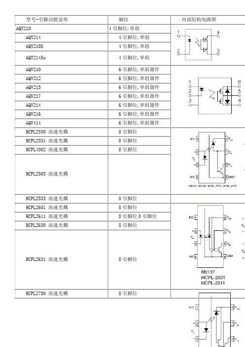
6 引脚位,单组器件 8 引脚位 8 引脚位 8 引脚位
ILD74 三极管输出
6,8,16 引脚位,4 组器 件
ILQ1 三极管输出 ILQ2 三极管输出
16 引脚位,4 组器件 16 引脚位,4 组器件
ILQ5 三极管输出
16 引脚位,4 组器件
ILQ74 三极管输出 IS201 三极管输出型 IS202 三极管输出型 IS203 三极管输出型 IS204 三极管输出型 IS205 三极管输出 IS205-1 三极管输出型光电藕合器件 IS205-2 三极管输出型光电藕合器件 IS206 三极管输出
H11D1 高耐压三极管输出 H11D2 高耐压三极管输出 H11D3 高耐压三极管输出 H11D4 高耐压三极管输出 H11F1 场效应管对称输出 H11F2 场效应管对称输出
6 引脚位,单组器件 6 引脚位,单组器件 6 引脚位,单组器件 6 引脚位,单组器件 6 引脚位,单组器件 6 引脚位,单组器件
6 引脚位,单组器件 6 引脚位,单组器件 6 引脚位,单组器件 6 引脚位,单组器件 6 引脚位,单组器件
4 引脚位,单组 4 引脚位,单组 4 引脚位,单组 4 引脚位,单组 引脚 6 引脚位,单组器件 6 引脚位,单组器件 6 引脚位,单组器件 内部结构图
IL74 三极管输出型 ILD1 三极管输出 ILD2 三极管输出 ILD5 三极管输出
4N40 单向晶闸管输出
6 引脚位,单组器件
6N135 高速光耦,高速光耦
6N136 高速光耦
6N137 逻辑高速输出 TTL 兼容
6N138 高增益高速光耦
6N139 高增益高速光耦
CNX62A 三极管输出
6 引脚位,单组器件
TLP701场管输出光藕

查询供应商
TLP701
TOSHIBA Photocoupler GaAℓAs IRED + Photo IC
TLP701
Industrial inverters Inverter for air conditioners IGBT/Power MOS FET gate drive
TLP701 consists of a GaAℓAs light-emitting diode and an integrated photodetector.
• Supply current
: 2 mA (max)
• Power supply voltage
: 10 to 30 V
• Threshold input current
: IFLH = 5 mA (max)
• Switching time (tpLH / tpHL)
: 700 ns (max)
• Common mode transient immunity
: ±10 kV/µs (min)
• Isolation voltage
: 5000 Vrms (min)
• Construction mechanical rating
7.62-mm pitch standard type
10.16-mm pitch TLPXXXF type
tlp2355原理
tlp2355原理
tlp2355是一种光耦合器件,也被称为光电耦合器。
它通常由
发光二极管(LED)和光敏二极管(光探测器)组成。
其工作原理是
利用LED发出的光信号照射到光敏二极管上,从而实现输入和输出
之间的电气隔离和信号传输。
从LED的角度来看,当LED端施加电压时,LED会发出光信号。
这个光信号经过光耦合器中的隔离层传播到光敏二极管的光敏区域。
光敏二极管的光敏区域会吸收LED发出的光信号,产生电荷载流子,从而在光敏二极管中产生电流或电压信号。
这个电流或电压信号可
以视为光耦合器的输出信号。
从电气隔离的角度来看,光耦合器实现了输入和输出之间的电
气隔离。
这是因为LED和光敏二极管之间的信号传输是通过光信号
而不是直接的电气连接。
这种电气隔离可以带来很多优势,比如可
以防止输入端的电气噪声传播到输出端,提高系统的稳定性和安全性。
总的来说,tlp2355光耦合器的工作原理涉及LED发出光信号,光信号经过隔离层照射到光敏二极管上,光敏二极管产生对应的电
流或电压信号,实现输入和输出之间的电气隔离和信号传输。
这种器件在工业控制、通信设备和医疗器械等领域有着广泛的应用。
TLP152原装东芝光藕中文资料及电路图
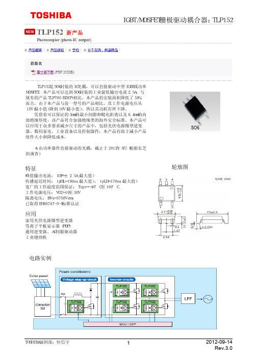
家用光伏电源微型逆变器 等离子平板显示器(PDP) 通用逆变器、AC伺服驱动器 工业缝纫机
电路实例
轮廓图
TOSHIBA深圳部:恒信宇
1
2012-09-14 Rev.3.0
IGBT/MOSFET栅极驱动耦合器:TLP152
TLP152是SO6封装的IC光耦,可以直接驱动中型IGBT或功率 MOSFET。本产品可以达到SO6封装的工业最低输出电流2.5A。与 现有的产品TLP700(SDIP)相比,本产品的安装面积降低了50%。 而且,由于本产品与前一型号的产品相比,其工作电源电压从 15V(最小值)降到10V(最小值),所以其功耗有所下降。 凭借着可以保证的5mm的最小间隙和爬电距离以及0.4mm的内 部绝缘厚度,该产品符合加强绝缘类的海外安全标准。本产品可 以应用于众多要求减少尺寸的产品中,包括光伏电源微型逆变 器、数码家电、工业设备以及控制器件,本产品有助于减小产品 组件大小和降低成本。 *:由功率器件直接驱动的光耦,截止于2012年9月(根据东芝 的调查)
特征
峰值输出电流:IOP=±2.5A(最大值) 传播延迟时间:tpHL=190ns(最大值), tpLH=170ns(最大值) 宽广的工作温度范围保证: Topr=-40°C至100°C 工作电源电压:VCC=10至30V 隔离电压:BVs=3750Vrms 已取得EN60747-5-5标准认证
光耦问题大解决

最近在使用光耦的时候遇到几个问题恳请指教?小生在使用光耦的时候遇到几个问题,恳请大侠指教:1:CTR(50%-300%)是什么意思?在电路中这个CTR是多少?与If有关吗?2:光耦的工作方式是电流控制还是电压控制。
最近在PS2561与TL431配合稳压反馈的电路中,外部参数怎么调整光耦都在正常工作,很费解。
3:希望有大侠分享光耦的使用心得。
潮光光耦网答:1、CTR(50%-300%)是电流传输比,CTR(Curremt-Trrasfer Ratio),它等于直流输出电流IC与直流输入电流IF的百分比。
简单来讲,就是个电流放大系数。
50%-600%是该系列光耦的CTR,在电路中是多少要看你选择的是哪个光耦。
? 2、光耦是电流控制的,你调节外部参数还在那个工作的范围里面,肯定可以工作啊,如果你把限流的电阻加很大就会出问题了。
? 3、CTR是电流传输比Ice/If我知道。
但是在具体电路中CTR的值是变化的还是固定的呢。
我用的光耦是NEC的PS2561,W系列。
传输比是130%-260%,看规格书是说CTR与If有关,是吗?另外我也想知道怎么来测量光耦的传输比。
在这个电路中,我通过改变R425的阻值,从100R改变为15K,光耦均能正常工作,R426两端的电压维持在1V。
当R425=100R的时候,Vk=22.9V,计算得出流过光耦的电流为1.1mA;当R425=15K的时候,Vk=3.68V,计算得出流过光耦的电流为0.13mA.这个电流变化还是很大的,但是光耦正常工作。
关于东芝光耦缺货型号,瑞萨(原NEC)光耦替代方案.关于东芝光耦缺货型号,潮光光耦网()建议各位采购和技术人员,瑞萨(原NEC)光耦替代方案另外还有很多高速光耦型号的替代详情登录光耦器件在变频器电路中的作用一、电路中为什么要使用光耦器件?电气隔离的要求。
A与B电路之间,要进行信号的传输,但两电路之间由于供电级别.一、电路中为什么要使用光耦器件?电气隔离的要求。
东芝TLP620,TLP620-2,TLP620-4光耦合器说明书
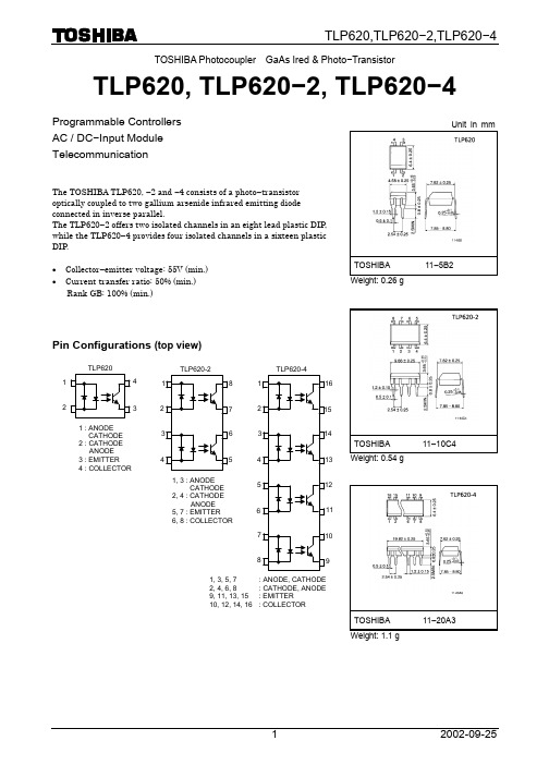
TOSHIBA Photocoupler GaAs Ired & Photo−TransistorTLP620, TLP620−2, TLP620−4Programmable ControllersAC / DC−Input ModuleTelecommunicationThe TOSHIBA TLP620, −2 and −4 consists of a photo−transistoroptically coupled to two gallium arsenide infrared emitting diodeconnected in inverse parallel.The TLP620−2 offers two isolated channels in an eight lead plastic DIP,while the TLP620−4 provides four isolated channels in a sixteen plasticDIP.· Collector−emitter voltage: 55V (min.)· Current transfer ratio: 50% (min.)Rank GB: 100% (min.)Pin Configurations (top view)TLP6201 2431 : ANODECATHODE2 : CATHODEANODE3 : EMITTER4 : COLLECTOR1, 3 : ANODECATHODE2, 4 : CATHODEANODE5, 7 : EMITTER6, 8 : COLLECTOR234561, 3, 5, 7 : ANODE, CATHODE2, 4, 6, 8 : CATHODE, ANODE9, 11, 13, 15 :EMITTER10, 12, 14, 16 : COLLECTORTOSHIBA 11−5B2Weight: 0.26 gTOSHIBA 11−10C4Weight: 0.54 gTOSHIBA 11−20A3Weight: 1.1 gUnit in mmMade In Japan Made In Thailand UL recognized E67349 *1E 152349 *1BSI approved7426, 7427*27426, 7427*2*1 UL 1577*2 BS EN60065: 1994, BS EN60950: 1992· Isolation voltage: 5000V rms (min.)· Option (D4) typeVDE approved: DIN VDE0884 / 06.92, certificate no. 68384 Maximum operating insulation voltage: 890V PK Highest permissible over voltage: 8000V PK(Note) When a VDE0884 approved type is needed,please designate the “Option(D4)”.· Creepage distance: 6.4mm (min.)Clearance: 6.4mm (min.)Insulation thickness: 0.4mm (min.)Maximum Ratings (Ta = 25°C)RatingCharacteristic SymbolTLP620TLP620-2 TLP620-4UnitForward current I F (RMS) 60 50 mAForward current derating ∆I F / °C -0.7 (Ta ≥ 39°C)-0.5 (Ta ≥ 25°C)mA / °CPulse forward current I FP 1 (100µs pulse, 100pps) APower dissipation (1 circuit) P D 100 70 mW Power dissipation derating ∆P D / °C-1.0-0.7 mW / °CL E DJunction temperature T j125 °CCollector -emitter voltage V CEO 55 VEmitter -collector voltage V ECO 7 VCollector currentI C 50 mA Collector power dissipation (1 circuit)P C 150 100 mW Collector power dissipation derating (1 circuit) (Ta ≥ 25°C) ∆P C / °C-1.5-1.0 mW / °CD e t e c t o rJunction temperature T j 125 °CStorage temperature range T stg -55~125 °COperating temperature range T opr-55~100 °CLead soldering temperature T sold 260 (10s) °C Total package power dissipation P T 250 150 mW Total package power dissipation derating (Ta ≥ 25°C, 1 circuit) ∆P T / °C-2.5-1.5 mW / °CIsolation voltageBV S 5000 (AC, 1 min., RH ≤ 60%)V rmsRecommended Operating ConditionsCharacteristic Symbol Min.Typ.Max.UnitSupply voltage V CC ― 5 24 V Forward current I F (RMS) ― 16 20 mA Collector current IC ― 110 mAOperating temperatureT opr-25― 85 °CIndividual Electrical Characteristics (Ta = 25°C)Characteristic Symbol Test Condition Min. Typ. Max.UnitForward voltage V F I F = ±10mA 1.01.151.3 VFoward currentI FV F = ±0.7V ― 2.5 20 µA L E DCapacitance C T V = 0, f = 1MHz ― 60 ― pF Collector -emitterbreakdown voltage V (BR) CEO I C = 0.5mA55―― VEmitter -collector breakdown voltage V (BR) ECOI E = 0.1mA 7 ― ― V V CE = 24V―10100nACollector dark current I CEO V CE = 24V, Ta = 85°C ― 2 50 µA D e t e c t o rCapacitance(collector to emitter)C CEV CE = 0, f = 1MHz―10― pFCoupled Electrical Characteristics (Ta = 25°C)Characteristic Symbol Test Condition MIn. Typ. Max.Unit50 ― 600Current transfer ratioI C / I FI F = ±5mA, V CE = 5V Rank GB100― 600%― 60 ― Saturated CTRI C / I F (sat)IF = ±1mA, V CE = 0.4V Rank GB30 ――%I C = 2.4mA, I F = ±8mA―― 0.4― 0.2 ― Collector -emitter saturation voltageV CE (sat)I C = 0.2 mA, I F = ±1 mA Rank GB― ― 0.4 VOff -state collector current I C (off) V F = ± 0.7V, V CE = 24V ― 110 µACTR symmetryI C (ratio)I C (I F = -5mA) / I C (I F = +5mA)0.331 3 ―Isolation Characteristics (Ta = 25°C)Characteristic Symbol Test Condition Min. Typ. Max.UnitCapacitance input tooutputC S V S = 0, f = 1MHz ― 0.8 ― pF Isolation resistanceR SV S = 500V 1×10¹² 1014 ― Ω AC, 1 minute5000 ― ― AC, 1 second, in oil ― 10000 ― V rms Isolation voltageBV SDC, 1 minute, in oil―10000―V dcSwitching Characteristics (Ta = 25°C)Characteristic Symbol Test Condition Min. Typ. Max.UnitRise time tr ― 2 ―Fall time t f ― 3 ― Turn -on time t on ― 3 ― Turn -off time t off V CC = 10V I C = 2mA R L = 100Ω― 3 ― µsTurn -on time t ON ― 2 ― Storage time t s ―15―Turn -off timet OFFR L = 1.9k Ω (Fig.1)V CC = 5V, I F = ±16mA ― 25 ―µsFig. 1 Switching time test circuitI FV CCV CECCTLP620-2 TLP620-4 I F – TaAmbient temperature Ta (°C)A l l o w a b l e f o r w a r d c u r r e n t I F (R M S ) (m A )100-2060400 20 40 60 80 100 8020120TLP620 P C – TaAmbient temperature Ta (°C)A l l o w a b l e c o l l e c t o r p o w e r d i s s i p a t i o n P C (m W )240-20 4016060100120080200120204080TLP620-2 TLP620-4 P C – TaAmbient temperature Ta (°C)A l l o w a b l e c o l l e c t o r p o w e r d i s s i p a t i o n P C (m W )1200-20400 40 10080602020 60 80 100 120TLP620 I FP – D RDuty cycle ratio D R A l l o w a b l e p u l s e f o r w a r d c u r r e n t I F P (m A )1 310311 3 3TLP620-2 TLP620-4 I FP – D RDuty cycle ratio D RA l l o w a b l e p u l s e f o r w a r d c u r r e n t I FP (m A )111 310 310 3100103TLP620 I F – TaAmbient temperature Ta (°C) A l l o w a b l e f o r w a r d c u r r e n t I F (R M S ) (m A )0-208040200 20 40 60 8010060100120∆V F / ∆Ta – I FForward current I F (mA)F o r w a r d v o l t a g e t e m p e r a t u r e c o e f f i c i e n t ∆V F / ∆T a (m V/ °C ) 1-2.8-2.4-2.0-1.6-1.2-0.8-0.40.10.331030I D – T aAmbient temperature Ta (°C)C o l l e c t o r d a r k c u r r e n t ID (µA )4080120160101010-10-10-10-I FP – V FPPulse forward voltage V FP (V)P u l s e f o r w a r d c u r r e n t I F P (m A )1100.40.81.21.6 2.01 2.4C o l l e c t o r c u r r e n t I C (m A )I C – V CECollector-emitter voltage V CE (V)C o l l e c t o r c u r r e n t I C (m A )24610I F – V FForward voltage V F (V) F o r w a r d c u r r e n tI F (m A )110.0.40.60.81.01.21.41.6I C – V CECollector-emitter voltage V CE(V)1100.40.61.4V F – I FForward voltage V F (V)F o r w a r d v o l t a g e I F (m A )-- 20.313103010011I C / I F – I FForward current I F (mA)C u r r e n t t r a n s f e r r a t i o I C / I F (%)I C – V FForward voltage V F (V)C o l l e c t o r c u r r e n t I C (m A )110.0.0I C – I FForward current I F (mA) C o l l e c t o r c u r r e n t I C (m A )110.I C – TaAmbient temperature Ta (°C)110. C o l l e c t o r c u r r e n t I C (mA )1111R L – Switching TimeLoad resistance R L (k Ω)S w i t c h i n g t i m e (µs )V CE (sat) – TaAmbient temperature Ta (°C)C o l l e c t o r -e m i t t e r s a t u r a t i on v o l t a g e V C E (s a t ) (V )2040600.10.10· TOSHIBA is continually working to improve the quality and reliability of its products. Nevertheless, semiconductor devices in general can malfunction or fail due to their inherent electrical sensitivity and vulnerability to physical stress. It is the responsibility of the buyer, when utilizing TOSHIBA products, to comply with the standards of safety in making a safe design for the entire system, and to avoid situations in which a malfunction or failure of such TOSHIBA products could cause loss of human life, bodily injury or damage to property.In developing your designs, please ensure that TOSHIBA products are used within specified operating ranges as set forth in the most recent TOSHIBA products specifications. Also, please keep in mind the precautions and conditions set forth in the “Handling Guide for Semiconductor Devices,” or “TOSHIBA Semiconductor Reliability Handbook” etc.. · The TOSHIBA products listed in this document are intended for usage in general electronics applications (computer, personal equipment, office equipment, measuring equipment, industrial robotics, domestic appliances, etc.). These TOSHIBA products are neither intended nor warranted for usage in equipment that requires extraordinarily high quality and/or reliability or a malfunction or failure of which may cause loss of human life or bodily injury (“Unintended Usage”). Unintended Usage include atomic energy control instruments, airplane or spaceship instruments, transportation instruments, traffic signal instruments, combustion control instruments, medical instruments, all types of safety devices, etc.. Unintended Usage of TOSHIBA products listed in this document shall be made at the customer’s own risk. · Gallium arsenide (GaAs) is a substance used in the products described in this document. GaAs dust and fumes are toxic. Do not break, cut or pulverize the product, or use chemicals to dissolve them. When disposing of the products, follow the appropriate regulations. Do not dispose of the products with other industrial waste or with domestic garbage. · The products described in this document are subject to the foreign exchange and foreign trade laws.· The information contained herein is presented only as a guide for the applications of our products. No responsibility is assumed by TOSHIBA CORPORATION for any infringements of intellectual property or other rights of the third parties which may result from its use. No license is granted by implication or otherwise under any intellectual property or other rights of TOSHIBA CORPORATION or others. · The information contained herein is subject to change without notice.000707EBCRESTRICTIONS ON PRODUCT USEThis datasheet has been download from: Datasheets for electronics components.。
友台半导体UMW TLP181小型光电耦合器说明书
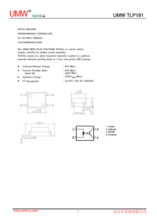
OFFICE MACHINEPROGRAMMABLE CONTROLLERSAC/DC-INPUT MODULETELECOMMUNICATIONThe UMW MINI FLAT COUPLER TLP181 is a small outline coupler, suitable for surface mount assembly.TLP181 consist of a photo transistor optically coupled to a gallium arsenide infrared emitting diode in a four lead plastic DIP package.•Collector-Emitter Voltage •Current Transfer RatioRank GB •Isolation Voltage•UL Recog nized : 80V(M in.): 50%(Min.): 100%(Min.): 3750V nn s (Min.): UL1577, File No. E4924401: Anode3: Cathode4: Emitter6: CollectorCURRENT TRANSFER RATIOCLASSI-�URRENT TRANSFER RATIO(%)(I r,/ I F)TYPE FICATION I F=5mA, V c E=5V, T a=25°C*1MIN. MAX.(None) 50 600Rank Y 50 150 TLP181 Rank GR 100 300Rank B L 200 600Rank GB 100 600*1 : EX, R ank GB : UM W TLP181 G B MARKIN G OF CLASSIFICATION B LANK, Y, Y曰G,G•,B,B•,GB Y, y■G,G•B,B■G,G•,B,B•,GBMAXIMUM RATINGS (Ta= 25°C)CHARACTERISTICF orward Current目占F orward Current DetatingPulse F orward CurrentReverse VoltageJunction TemperatureCollector-Emitter Voltage恳Emitter-Collector VoltageCollector Current且仁Collector Power Dissipation (1 Circuit) Collector Power Dissipation Derating(1 Circuit Ta�25°0)Junction TemperatureStorage Temperature RangeOperating Temperature Range Lead Soldering TemperatureTotal Package Power DissipationTotal Package Power Dissipation Derating (Ta�25°C) Isolation Voltage(Note 1)SYM B OL I FL1I F / o c l F P V R T j V c EO V ECOI c P cL1P c 1°c T i T stgT 。
东芝TLP350F光耦合器数据表说明书

TOSHIBA Photocoupler GaA ℓAs IRED + Photo ICTLP350FIndustrial InverterInverter for Air ConditionerIGBT/Power MOSFET Gate Drive IH(Induction Heating)The TOSHIBA TLP350F consists of a GaA ℓAs light-emitting diode and an integrated photodetector.This unit is an 8-lead DIP package.The TLP350F is suitable for gate driving IGBTs or power MOSFETs.Absolute maximum ratings and electrical characteristics are the same as TLP350technical datasheet.• Peak output current: I O = ±2.5A (max)• Guaranteed performance over temperature: −40 to 100°C • Supply current:I CC = 2 mA (max) • Power supply voltage: V CC = 15 to 30 V • Threshold input current : I FLH = 5 mA (max) • Switching time (t pLH /t pHL ) : 500 ns (max) • Common mode transient immunity: 15 kV/μs • Isolation voltage: 3750 Vrms• UL Recognized : UL1577,File No.E67349 • Option(D4)VDE Approved : DIN EN 60747-5-2Maximum Operating Insulation Voltage : 1140V PK Highest Permissible Over Voltage : 6000V PK (Note): When an EN60747-5-2 approved type is needed, Please designate “Option(D4)”• Construction mechanical ratingTruth Table Input LED Tr1 Tr2 Output H ON ON OFF H LOFF OFF ONLUnit: mmTOSHIBA 11-10C402 Weight: 0.54 g (typ.)81: NC 2: Anode 3: Cathode 4: NC 5: GND6: V O (output)7: NC 8: V CC7 6 51234A 0.1 μF bypass capacitor must be connected between pins 8 and 5. (See Note 6)2+3−V CCV OGND(Tr1)(Tr2) I CC I O I FV F8657.62mm pitch TLP350 type 10.16mm pitch TLP350F type Creepage distance ClearanceInsulation thickness6.4 mm (min) 6.4 mm (min) 0.4 mm (min) 8.0 mm (min) 8.0 mm (min) 0.4 mm (min)Pin Configuration (top view)SchematicRESTRICTIONS ON PRODUCT USE20070701-EN •The information contained herein is subject to change without notice.•TOSHIBA is continually working to improve the quality and reliability of its products. Nevertheless, semiconductor devices in general can malfunction or fail due to their inherent electrical sensitivity and vulnerability to physical stress. It is the responsibility of the buyer, when utilizing TOSHIBA products, to comply with the standards of safety in making a safe design for the entire system, and to avoid situations in which a malfunction or failure of such TOSHIBA products could cause loss of human life, bodily injury or damage to property.In developing your designs, please ensure that TOSHIBA products are used within specified operating ranges as set forth in the most recent TOSHIBA products specifications. Also, please keep in mind the precautions and conditions set forth in the “Handling Guide for Semiconductor Devices,” or “TOSHIBA Semiconductor Reliability Handbook” etc.• The TOSHIBA products listed in this document are intended for usage in general electronics applications (computer, personal equipment, office equipment, measuring equipment, industrial robotics, domestic appliances, etc.).These TOSHIBA products are neither intended nor warranted for usage in equipment that requires extraordinarily high quality and/or reliability or a malfunction or failure of which may cause loss of human life or bodily injury (“Unintended Usage”). Unintended Usage include atomic energy control instruments, airplane or spaceship instruments, transportation instruments, traffic signal instruments, combustion control instruments, medical instruments, all types of safety devices, etc.. Unintended Usage of TOSHIBA products listed in his document shall be made at the customer’s own risk.•The products described in this document shall not be used or embedded to any downstream products of which manufacture, use and/or sale are prohibited under any applicable laws and regulations.• The information contained herein is presented only as a guide for the applications of our products. No responsibility is assumed by TOSHIBA for any infringements of patents or other rights of the third parties which may result from its use. No license is granted by implication or otherwise under any patents or other rights of TOSHIBA or the third parties.•GaAs(Gallium Arsenide) is used in this product. The dust or vapor is harmful to the human body. Do not break, cut, crush or dissolve chemically.• Please contact your sales representative for product-by-product details in this document regarding RoHS compatibility. Please use these products in this document in compliance with all applicable laws and regulations that regulate the inclusion or use of controlled substances. Toshiba assumes no liability for damage or losses occurring as a result of noncompliance with applicable laws and regulations.。
- 1、下载文档前请自行甄别文档内容的完整性,平台不提供额外的编辑、内容补充、找答案等附加服务。
- 2、"仅部分预览"的文档,不可在线预览部分如存在完整性等问题,可反馈申请退款(可完整预览的文档不适用该条件!)。
- 3、如文档侵犯您的权益,请联系客服反馈,我们会尽快为您处理(人工客服工作时间:9:00-18:30)。
恒信宇电子仪表电器元件器材配套:集成电路IC、二三极管、光电藕合器、可控硅、LED电源驱动IC……
TLP181可一采用TLP185进行替代
由于使用了S06封装,TLP184 和TLP185晶体管耦合器比前一代产品要轻薄,而且能在高温
下正常工作(Ta = 110度最大值)。
TLP184 和TLP185分别是TLP180 and TLP181的更新产品。
能轻易用这些产品代替现在的这些型号,因为这些产品的参考衰减器尺寸与现在的MFSOP6封装型号的尺寸是一样的。
而且,由于更轻薄,这些产品能将安装高度从先前的2.8毫米,降低到2.3毫米。
因为SO6封装能确保最小的间隙和爬电距离为5毫米,而不是现有型号MFSOP6封装中的4毫米。
所以这些产品的最大允许操作隔离电压为707 Vpk,EN60747-5-2中已明确规定过。
所以,TLP184 和TLP185能更换DIP封装区域的零件(TLP781,TLP785等)。
而且,这种产品能确保内部绝缘厚度为0.4毫米,而且属于加强绝缘种类,符合国外安全标准。
因为这些产品都达到了UL、cUL、VDE及BSI等国际认证的安全标准,所以他们非常适合AC 适配器、开关电源供电及FA设备等电子应用场合。
TLP785/TLP781代替TLP521/TLP421/TLP621
TLP785/TLP781是东芝TOSHIBA研发的TLP521/TLP421/TLP621升级版,并将逐步取代TLP521/TLP421/TLP621的生产。
恒信宇Emal:jsong820@。