A 10-Gbps CDR-DEMUX with LC delay line VCO in 0.18-spl mu-m CMOS
SLVU2.8-4中文资料
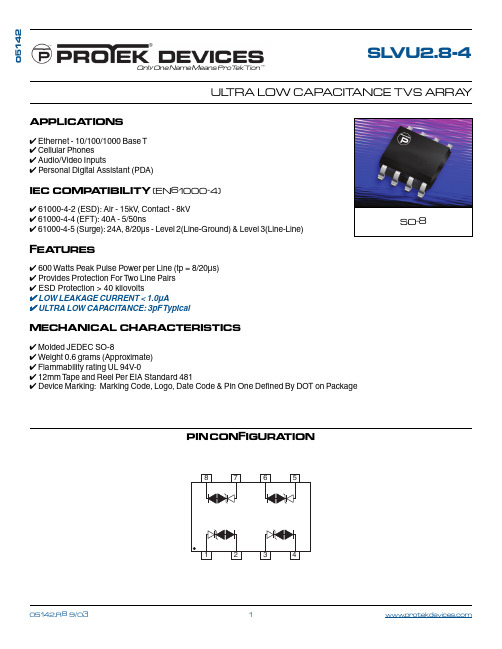
SL VU2.8-4UL TRA LOW CAP ACIT ANCE TVS ARRA YOnly One Name Means ProTek’Tion™APPLICA TIONS ✔ Ethernet - 10/100/1000 Base T✔ Cellular Phones ✔ Audio/Video Inputs✔ Personal Digital Assistant (PDA)IEC COMP A TIBILITY (EN61000-4)✔ 61000-4-2 (ESD): Air - 15kV , Contact - 8kV ✔ 61000-4-4 (EFT): 40A - 5/50ns✔ 61000-4-5 (Surge): 24A, 8/20µs - Level 2(Line-Ground) & Level 3(Line-Line)FEA TURES✔ 600 Watts Peak Pulse Power per Line (tp = 8/20µs)✔ Provides Protection For Two Line Pairs ✔ ESD Protection > 40 kilovolts✔ LOW LEAKAGE CURRENT < 1.0µA✔ ULTRA LOW CAPACITANCE: 3pF T ypicalMECHANICAL CHARACTERISTICS✔ Molded JEDEC SO-8✔ Weight 0.6 grams (Approximate)✔ Flammability rating UL 94V-0✔ 12mm Tape and Reel Per EIA Standard 481✔ Device Marking: Marking Code, Logo, Date Code & Pin One Defined By DOT on Package05142PIN CONFIGURA TIONSO-8DEVICE CHARACTERISTICSMAXIMUM RA TINGS @ 25°C Unless Otherwise SpecifiedPeak Pulse Power (t p = 8/20µs) - See Figure 1Peak Pulse Current (t p = 8/20µs)Lead Soldering T emperature Operating T emperature SYMBOL VALUE -55°C to 150°C°C°C -55°C to 150°C °C Amps Watts UNITS 260°C (10s)600T J I FRM I PP P PP P ARAMETERStorage T emperature30T STGELECTRICAL CHARACTERISTICS PER LINE @ 25°C Unless Otherwise Specified21TYPICAL CAP ACIT ANCE (See Note 1)@0V , 1MHzC pF1.03MAXIMUM CLAMPING VOL T AGE (See Note 1)(See Fig. 2)@I P = 30AV C VOL TSMAXIMUM LEAKAGE CURRENT (See Note 1)@V WMI D µA Note 1: Device measured between pin 1 to 2, pin 3 to 4, pin 5 to 6 and pin 7 to 8.MAXIMUM CLAMPING VOL T AGE (See Note 1)(See Fig. 2)@I P = 5A V C VOL TS 8.55.5MAXIMUM CLAMPING VOL T AGE (See Note 1)(See Fig. 2)@I P = 2A V C VOL TS MINIMUM SNAPBACK VOL T AGE (See Note 1)@I SB = 50mAV SB VOL TS2.83.02.8SL4SLVU2.8-4P ARTNUMBERDEVICE MARKING CODERA TED ST AND-OFF VOL T AGE (See Note 1)V WM VOL TSMINIMUM BREAKDOWN VOL T AGE (See Note 1)@ 1mA V (BR)VOL TS MAXIMUM CLAMPING VOL T AGE (See Note 1)(See Fig. 2)@I P = 24AV C VOL TS15GRAPHSFIGURE 20 5 10 15 20 25 30t - Time - µs20406080100120I P P - P e a k P u l s e C u r r e n t - % o f I P PFIGURE 1PEAK PULSE POWER VS PULSE TIME0.01 1 10 100 1,000 10,000t d - Pulse Duration - µs101001,00010,000P P P - P e a k P u l s e C u r r e n t - W a t t sT L - Lead Temperature - °C20406080100% O f R a t e d P o w e rFIGURE 3ypical Clamping Voltage vs Peak Pulse Curren 06284PIN 2 TO 1PIN 3 TO 1APPLICA TION NOTEElectronic equipment is susceptible to damage caused by Electrostatic Discharge (ESD), Electrical Fast T ransients (EFT), and tertiary lightning effects. Knowing that equipment can be damaged, the SLVU2.8-4 was designed to provide the level of protection required to safe guard sensitive equipment. This product can be used in different configurations to provide a level of protection to meet unidirectional line requirements as well as bidirectional requirements either in a common-mode or differential-mode configuration.UNIDIRECTIONAL DIFFERENTIAL-MODE CONFIGURATION (Figure 1)depicted in figure 1.Circuit connectivity is as follows:✔Line 1 is connected to Pin 1✔Line 2 is connected to Pin 7✔Line 3 is connected to Pin 3✔Line 4 is connected to Pin 5✔Pins 2, 4, 7 and 8 are connected to groundBIDIRECTIONAL COMMON-MODE CONFIGURATION (Figure 2)depicted in figure 1.Circuit connectivity is as follows:✔Line 1 is connected to Pins 1 & 8✔Line 2 is connected to Pins 4 & 5✔Pins 2, 3, 6, and 7 are connected to groundBIDIRECTIONAL DIFFERENTIAL-MODE CONFIGURATION (Figure 3) depicted in figure 1.External diode to ground is a low capacitance diode of less than 10pFCOPYRIGHT © ProTek Devices 2003SPECIFICA TIONS: ProT ek reserves the right to change the electrical and or mechanical characteristics described herein without notice (except JEDEC).DESIGN CHANGES: ProT ek reserves the right to discontinue product lines without notice, and that the final judgement concerning selection and specifications is the buyer’s and that in furnishing engineering and technical assistance, ProTek assumes no responsibility with respect to the selection or specifications of such products.P ACKAGE OUTLINE & DIMENSIONSProTek Devices2929 South Fair Lane, Tempe, AZ 85282Tel: 602-431-8101 Fax: 602-431-2288E-Mail: sales@ Web Site: 。
AD9783中文资料

CLKP CLKN
LVDS INTERFAቤተ መጻሕፍቲ ባይዱE
D[15:0] VIA, VIB
DEINTERLEAVING LOGIC
Full programmability is provided through a serial peripheral interface (SPI) port. Some pin-programmable features are also offered for those applications without a controller.
Dual 12-/14-/16-Bit,
LVDS Interface, 500 MSPS DACs
AD9780/AD9781/AD9783
GENERAL DESCRIPTION
The AD9780/AD9781/AD9783 include pin-compatible, high dynamic range, dual digital-to-analog converters (DACs) with 12-/14-/16-bit resolutions, and sample rates of up to 500 MSPS. The devices include specific features for direct conversion transmit applications, including gain and offset compensation, and they interface seamlessly with analog quadrature modulators such as the ADL5370.
Keysight E4980A AL Precision LCR Meter 用户指南说明书
Keysight E4980A/AL Precision LCR MeterUser’s GuideNotices© Keysight Technologies2006-2019No part of this manual may be reproduced in any form or by any means (including electronic storage and retrieval or translation into a foreign language) without prior agreement and written consent from Keysight Technologies, Inc. as governed by United States and international copyright laws. Trademark Acknowledgments Manual Part NumberE4980-90230EditionEdition 16, October 2019 Printed in MalaysiaPublished by:Keysight Technologies International Japan G.K,1-3-3 Higashikawasaki-choChuo-kuKobe-shi, Hyogo, Japan WarrantyTHE MATERIAL CONTAINED IN THIS DOCUMENT IS PROVIDED “AS IS,” AND IS SUBJECT TO BEING CHANGED, WITHOUT NOTICE, IN FUTURE EDITIONS. FURTHER, TO THE MAXIMUM EXTENT PERMITTED BY APPLICABLE LAW, KEYSIGHT DISCLAIMS ALL WARRANTIES, EITHER EXPRESS OR IMPLIED WITH REGARD TO THIS MANUAL AND ANY INFORMATION CONTAINED HEREIN, INCLUDING BUT NOT LIMITED TO THE IMPLIED WARRANTIES OF MERCHANTABILITY AND FITNESS FOR A PARTICULAR PURPOSE. KEYSIGHT SHALL NOT BE LIABLE FOR ERRORS OR FOR INCIDENTAL OR CONSEQUENTIAL DAMAGES IN CONNECTION WITH THE FURNISHING, USE, OR PERFORMANCE OF THIS DOCUMENT OR ANY INFORMATION CONTAINED HEREIN. SHOULD KEYSIGHT AND THE USER HAVE A SEPARATE WRITTEN AGREEMENT WITH WARRANTY TERMS COVERING THE MATERIAL IN THISDOCUMENT THAT CONFLICT WITHTHESE TERMS, THE WARRANTYTERMS IN THE SEPARATEAGREEMENT WILL CONTROL.Technology LicensesThe hardware and/or softwaredescribed in this document arefurnished under a license and may beused or copied only in accordancewith the terms of such license.Declaration of ConformityDeclarations of Conformity for thisproduct and for other Keysightproducts may be downloaded fromthe Web. Go to/go/conformity. You can then search by productnumber to find the latest Declarationof Conformity.U.S. Government RightsThe Software is “commercialcomputer software,” as defined byFederal Acquisition Regulation(“FAR”) 2.101. Pursuant to FAR12.212 and 27.405-3 andDepartment of Defense FARSupplement (“DFARS”) 227.7202, theU.S. government acquirescommercial computer softwareunder the same terms by which thesoftware is customarily provided tothe public. Accordingly, Keysightprovides the Software to U.S.government customers under itsstandard commercial license, whichis embodied in its End User LicenseAgreement (EULA), a copy of whichcan be found at/find/sweula. The license set forth in the EULArepresents the exclusive authority bywhich the U.S. government may use,modify, distribute, or disclose theSoftware. The EULA and the licenseset forth therein, does not require orpermit, among other things, thatKeysight: (1) Furnish technicalinformation related to commercialcomputer software or commercialcomputer software documentationthat is not customarily provided tothe public; or (2) Relinquish to, orotherwise provide, the governmentrights in excess of these rightscustomarily provided to the public touse, modify, reproduce, release,perform, display, or disclosecommercial computer software orcommercial computer softwaredocumentation. No additionalgovernment requirements beyondthose set forth in the EULA shallapply, except to the extent that thoseterms, rights, or licenses areexplicitly required from all providersof commercial computer softwarepursuant to the FAR and the DFARSand are set forth specifically inwriting elsewhere in the EULA.Keysight shall be under no obligationto update, revise or otherwise modifythe Software. With respect to anytechnical data as defined by FAR2.101, pursuant to FAR 12.211 and27.404.2 and DFARS 227.7102, theU.S. government acquires no greaterthan Limited Rights as defined in FAR27.401 or DFAR 227.7103-5 (c), asapplicable in any technical data.Safety NoticesA CAUTION notice denotes a hazard. Itcalls attention to an operatingprocedure, practice, or the like that,if not correctly performed or adheredto, could result in damage to theproduct or loss of important data. Donot proceed beyond a CAUTIONnotice until the indicated conditionsare fully understood and met.A WARNING notice denotes a hazard.It calls attention to an operatingprocedure, practice, or the like that,if not correctly performed or adheredto, could result in personal injury ordeath. Do not proceed beyond aWARNING notice until the indicatedconditions are fully understood andmet.ContentsKeysight E4980A/AL User’s Guide 3Table of Contents1.Unpacking and PreparationContents of this Chapter . . . . . . . . . . . . . . . . . . . . . . . . . . . . . . . . . . . . . . . . . . . . . . . . . . . . . 17Checking the Shipment . . . . . . . . . . . . . . . . . . . . . . . . . . . . . . . . . . . . . . . . . . . . . . . . . . . . . . 18Preparations before Use. . . . . . . . . . . . . . . . . . . . . . . . . . . . . . . . . . . . . . . . . . . . . . . . . . . . . . 20Verifying the Power Supply . . . . . . . . . . . . . . . . . . . . . . . . . . . . . . . . . . . . . . . . . . . . . . . . 20Setting up the Fuse . . . . . . . . . . . . . . . . . . . . . . . . . . . . . . . . . . . . . . . . . . . . . . . . . . . . . . 20Verifying and Connecting the Power Cable. . . . . . . . . . . . . . . . . . . . . . . . . . . . . . . . . . . . 21How to Remove the Handle. . . . . . . . . . . . . . . . . . . . . . . . . . . . . . . . . . . . . . . . . . . . . . . . . . . 23Caution when Using the Handle . . . . . . . . . . . . . . . . . . . . . . . . . . . . . . . . . . . . . . . . . . . . . . . 24Environmental Requirements. . . . . . . . . . . . . . . . . . . . . . . . . . . . . . . . . . . . . . . . . . . . . . . . . . 25Operating Environments. . . . . . . . . . . . . . . . . . . . . . . . . . . . . . . . . . . . . . . . . . . . . . . . . . . 25Ventilation Requirements. . . . . . . . . . . . . . . . . . . . . . . . . . . . . . . . . . . . . . . . . . . . . . . . . . 26Protection Against Electrostatic Discharge (ESD). . . . . . . . . . . . . . . . . . . . . . . . . . . . . . . 27Ensuring Adequate Free Space around the LCR meter for Immediate Disconnection of the Power Cable in Case of Emergency. . . . . . . . . . . . . . . . . . . . . . . . . . . . . . . . . . . . . . . . . . 27Starting the E4980A/AL. . . . . . . . . . . . . . . . . . . . . . . . . . . . . . . . . . . . . . . . . . . . . . . . . . . . . . 28Turning the Power ON and OFF. . . . . . . . . . . . . . . . . . . . . . . . . . . . . . . . . . . . . . . . . . . . . 28Disconnecting from the Supply Source. . . . . . . . . . . . . . . . . . . . . . . . . . . . . . . . . . . . . . . 292.OverviewProduct Introduction. . . . . . . . . . . . . . . . . . . . . . . . . . . . . . . . . . . . . . . . . . . . . . . . . . . . . . . . . 31Front Panel: Names and Functions of Parts . . . . . . . . . . . . . . . . . . . . . . . . . . . . . . . . . . . . . . 321. Power switch . . . . . . . . . . . . . . . . . . . . . . . . . . . . . . . . . . . . . . . . . . . . . . . . . . . . . . . . . 332. LCD . . . . . . . . . . . . . . . . . . . . . . . . . . . . . . . . . . . . . . . . . . . . . . . . . . . . . . . . . . . . . . . . 333. Softkeys . . . . . . . . . . . . . . . . . . . . . . . . . . . . . . . . . . . . . . . . . . . . . . . . . . . . . . . . . . . . . 334. Menu keys. . . . . . . . . . . . . . . . . . . . . . . . . . . . . . . . . . . . . . . . . . . . . . . . . . . . . . . . . . . . 335. Cursor keys. . . . . . . . . . . . . . . . . . . . . . . . . . . . . . . . . . . . . . . . . . . . . . . . . . . . . . . . . . . 336. Entry keys. . . . . . . . . . . . . . . . . . . . . . . . . . . . . . . . . . . . . . . . . . . . . . . . . . . . . . . . . . . . 347. LED indicator . . . . . . . . . . . . . . . . . . . . . . . . . . . . . . . . . . . . . . . . . . . . . . . . . . . . . . . . . 348. Preset key. . . . . . . . . . . . . . . . . . . . . . . . . . . . . . . . . . . . . . . . . . . . . . . . . . . . . . . . . . . . 349. Trigger key . . . . . . . . . . . . . . . . . . . . . . . . . . . . . . . . . . . . . . . . . . . . . . . . . . . . . . . . . . . 3410. DC Bias key. . . . . . . . . . . . . . . . . . . . . . . . . . . . . . . . . . . . . . . . . . . . . . . . . . . . . . . . . . 3411. DC Source key . . . . . . . . . . . . . . . . . . . . . . . . . . . . . . . . . . . . . . . . . . . . . . . . . . . . . . . 3412. UNKNOWN terminals . . . . . . . . . . . . . . . . . . . . . . . . . . . . . . . . . . . . . . . . . . . . . . . . . 3513. Front USB port . . . . . . . . . . . . . . . . . . . . . . . . . . . . . . . . . . . . . . . . . . . . . . . . . . . . . . . 3514. Ground terminal. . . . . . . . . . . . . . . . . . . . . . . . . . . . . . . . . . . . . . . . . . . . . . . . . . . . . . 3615. DC Source terminal . . . . . . . . . . . . . . . . . . . . . . . . . . . . . . . . . . . . . . . . . . . . . . . . . . . 36Rear Panel: Names and Functions of Parts . . . . . . . . . . . . . . . . . . . . . . . . . . . . . . . . . . . . . . . 371. GPIB Interface Connector . . . . . . . . . . . . . . . . . . . . . . . . . . . . . . . . . . . . . . . . . . . . . . . 37Contents2. Interface Connector. . . . . . . . . . . . . . . . . . . . . . . . . . . . . . . . . . . . . . . . . . . . . . . . . . . . .373. USB (USBTMC) Interface Port. . . . . . . . . . . . . . . . . . . . . . . . . . . . . . . . . . . . . . . . . . . . .384. LAN Port . . . . . . . . . . . . . . . . . . . . . . . . . . . . . . . . . . . . . . . . . . . . . . . . . . . . . . . . . . . . .385. External Trigger Input Connector . . . . . . . . . . . . . . . . . . . . . . . . . . . . . . . . . . . . . . . . . .386. Serial Number Plate . . . . . . . . . . . . . . . . . . . . . . . . . . . . . . . . . . . . . . . . . . . . . . . . . . . .387. Power Cable Receptacle (to LINE) . . . . . . . . . . . . . . . . . . . . . . . . . . . . . . . . . . . . . . . . .398. Fan. . . . . . . . . . . . . . . . . . . . . . . . . . . . . . . . . . . . . . . . . . . . . . . . . . . . . . . . . . . . . . . . . .39Screen Area: Names and Functions of Parts. . . . . . . . . . . . . . . . . . . . . . . . . . . . . . . . . . . . . . .401. Display Page Area . . . . . . . . . . . . . . . . . . . . . . . . . . . . . . . . . . . . . . . . . . . . . . . . . . . . . .402. Comment Line Area. . . . . . . . . . . . . . . . . . . . . . . . . . . . . . . . . . . . . . . . . . . . . . . . . . . . .403. Softkey Area. . . . . . . . . . . . . . . . . . . . . . . . . . . . . . . . . . . . . . . . . . . . . . . . . . . . . . . . . . .414. Measurement Data/Conditions Area. . . . . . . . . . . . . . . . . . . . . . . . . . . . . . . . . . . . . . . .415. Input Line Area . . . . . . . . . . . . . . . . . . . . . . . . . . . . . . . . . . . . . . . . . . . . . . . . . . . . . . . .426. System Message Area. . . . . . . . . . . . . . . . . . . . . . . . . . . . . . . . . . . . . . . . . . . . . . . . . . .427. Status Display Area. . . . . . . . . . . . . . . . . . . . . . . . . . . . . . . . . . . . . . . . . . . . . . . . . . . . .42Basic Operation. . . . . . . . . . . . . . . . . . . . . . . . . . . . . . . . . . . . . . . . . . . . . . . . . . . . . . . . . . . . .43 How to Use Cursor Keys . . . . . . . . . . . . . . . . . . . . . . . . . . . . . . . . . . . . . . . . . . . . . . . . . . .43 How to Use Skip Keys. . . . . . . . . . . . . . . . . . . . . . . . . . . . . . . . . . . . . . . . . . . . . . . . . . . . .44 3.Display FormatMEAS DISPLAY Page. . . . . . . . . . . . . . . . . . . . . . . . . . . . . . . . . . . . . . . . . . . . . . . . . . . . . . . . .45 Measurement Function . . . . . . . . . . . . . . . . . . . . . . . . . . . . . . . . . . . . . . . . . . . . . . . . . . . .47 Impedance range. . . . . . . . . . . . . . . . . . . . . . . . . . . . . . . . . . . . . . . . . . . . . . . . . . . . . . . . .51 Test Frequency. . . . . . . . . . . . . . . . . . . . . . . . . . . . . . . . . . . . . . . . . . . . . . . . . . . . . . . . . . .58 Test Signal Level . . . . . . . . . . . . . . . . . . . . . . . . . . . . . . . . . . . . . . . . . . . . . . . . . . . . . . . . .61 DC Bias . . . . . . . . . . . . . . . . . . . . . . . . . . . . . . . . . . . . . . . . . . . . . . . . . . . . . . . . . . . . . . . .64 Measurement Time Mode . . . . . . . . . . . . . . . . . . . . . . . . . . . . . . . . . . . . . . . . . . . . . . . . . .68 Display Setting for Measurement Results. . . . . . . . . . . . . . . . . . . . . . . . . . . . . . . . . . . . . .69 Displaying Errors instead of Measurement Results . . . . . . . . . . . . . . . . . . . . . . . . . . . . . .71 Monitor Information. . . . . . . . . . . . . . . . . . . . . . . . . . . . . . . . . . . . . . . . . . . . . . . . . . . . . . .75 BIN NO. DISPLAY Page . . . . . . . . . . . . . . . . . . . . . . . . . . . . . . . . . . . . . . . . . . . . . . . . . . . . . . .76 Comparator Function ON/OFF . . . . . . . . . . . . . . . . . . . . . . . . . . . . . . . . . . . . . . . . . . . . . .77 BIN COUNT DISPLAY Page . . . . . . . . . . . . . . . . . . . . . . . . . . . . . . . . . . . . . . . . . . . . . . . . . . . .79 Counter Function. . . . . . . . . . . . . . . . . . . . . . . . . . . . . . . . . . . . . . . . . . . . . . . . . . . . . . . . .81 LIST SWEEP DISPLAY Page. . . . . . . . . . . . . . . . . . . . . . . . . . . . . . . . . . . . . . . . . . . . . . . . . . . .82 Sweep Mode . . . . . . . . . . . . . . . . . . . . . . . . . . . . . . . . . . . . . . . . . . . . . . . . . . . . . . . . . . . .84 DISPLAY BLANK Page. . . . . . . . . . . . . . . . . . . . . . . . . . . . . . . . . . . . . . . . . . . . . . . . . . . . . . . .86 4.Configuring Measurement Conditions (Display and Function Related Settings)Initializing the Instrument . . . . . . . . . . . . . . . . . . . . . . . . . . . . . . . . . . . . . . . . . . . . . . . . . . . . .87 MEAS SETUP page . . . . . . . . . . . . . . . . . . . . . . . . . . . . . . . . . . . . . . . . . . . . . . . . . . . . . . . . . .884 Keysight E4980A/AL User’s GuideContentsKeysight E4980A/AL User’s Guide 5Comment line. . . . . . . . . . . . . . . . . . . . . . . . . . . . . . . . . . . . . . . . . . . . . . . . . . . . . . . . . . . 90Trigger mode . . . . . . . . . . . . . . . . . . . . . . . . . . . . . . . . . . . . . . . . . . . . . . . . . . . . . . . . . . . 91Automatic level control . . . . . . . . . . . . . . . . . . . . . . . . . . . . . . . . . . . . . . . . . . . . . . . . . . . 93DC Bias Current Isolation. . . . . . . . . . . . . . . . . . . . . . . . . . . . . . . . . . . . . . . . . . . . . . . . . . 97Averaging Factor . . . . . . . . . . . . . . . . . . . . . . . . . . . . . . . . . . . . . . . . . . . . . . . . . . . . . . . . 98Trigger Delay Time . . . . . . . . . . . . . . . . . . . . . . . . . . . . . . . . . . . . . . . . . . . . . . . . . . . . . . . 99Step Delay Time. . . . . . . . . . . . . . . . . . . . . . . . . . . . . . . . . . . . . . . . . . . . . . . . . . . . . . . . 101DC Bias Voltage Monitor . . . . . . . . . . . . . . . . . . . . . . . . . . . . . . . . . . . . . . . . . . . . . . . . . 103DC Bias Current Monitor . . . . . . . . . . . . . . . . . . . . . . . . . . . . . . . . . . . . . . . . . . . . . . . . . 104DCR Range. . . . . . . . . . . . . . . . . . . . . . . . . . . . . . . . . . . . . . . . . . . . . . . . . . . . . . . . . . . . 105DCI Range. . . . . . . . . . . . . . . . . . . . . . . . . . . . . . . . . . . . . . . . . . . . . . . . . . . . . . . . . . . . . 106DC Source. . . . . . . . . . . . . . . . . . . . . . . . . . . . . . . . . . . . . . . . . . . . . . . . . . . . . . . . . . . . . 107Automatic Bias Polarity Control . . . . . . . . . . . . . . . . . . . . . . . . . . . . . . . . . . . . . . . . . . . 108Deviation Measurement. . . . . . . . . . . . . . . . . . . . . . . . . . . . . . . . . . . . . . . . . . . . . . . . . . 110CORRECTION page . . . . . . . . . . . . . . . . . . . . . . . . . . . . . . . . . . . . . . . . . . . . . . . . . . . . . . . . 112To set the correction function to on or off. . . . . . . . . . . . . . . . . . . . . . . . . . . . . . . . . . . . 113The correction functions of the E4980A/AL are operated as follows:. . . . . . . . . . . . . . . 114Open Correction. . . . . . . . . . . . . . . . . . . . . . . . . . . . . . . . . . . . . . . . . . . . . . . . . . . . . . . . 115Short Correction. . . . . . . . . . . . . . . . . . . . . . . . . . . . . . . . . . . . . . . . . . . . . . . . . . . . . . . . 119Correction Based on User-Specified Frequency Points. . . . . . . . . . . . . . . . . . . . . . . . . . 121Relationships between Correction Based on All Frequency Points and Correction Based on Specified Frequency Points . . . . . . . . . . . . . . . . . . . . . . . . . . . . . . . . . . . . . . . . . . . . . . . 128Reading/Writing Correction Data . . . . . . . . . . . . . . . . . . . . . . . . . . . . . . . . . . . . . . . . . . 130Measurement Functions for the Standard. . . . . . . . . . . . . . . . . . . . . . . . . . . . . . . . . . . . 131Selecting Single/Multiple Correction Mode . . . . . . . . . . . . . . . . . . . . . . . . . . . . . . . . . . 132Selecting the Cable Length . . . . . . . . . . . . . . . . . . . . . . . . . . . . . . . . . . . . . . . . . . . . . . . 133LIMIT TABLE SETUP Page . . . . . . . . . . . . . . . . . . . . . . . . . . . . . . . . . . . . . . . . . . . . . . . . . . . 134Parameter Swap Feature . . . . . . . . . . . . . . . . . . . . . . . . . . . . . . . . . . . . . . . . . . . . . . . . . 135Comparator Limit Mode. . . . . . . . . . . . . . . . . . . . . . . . . . . . . . . . . . . . . . . . . . . . . . . . . . 137Tolerance Mode Nominal Value. . . . . . . . . . . . . . . . . . . . . . . . . . . . . . . . . . . . . . . . . . . . 139Turning On/Off the Comparator. . . . . . . . . . . . . . . . . . . . . . . . . . . . . . . . . . . . . . . . . . . . 140Turning On/Off the Auxiliary Bin . . . . . . . . . . . . . . . . . . . . . . . . . . . . . . . . . . . . . . . . . . . 141Beep Feature . . . . . . . . . . . . . . . . . . . . . . . . . . . . . . . . . . . . . . . . . . . . . . . . . . . . . . . . . . 143Lower and Upper Limits . . . . . . . . . . . . . . . . . . . . . . . . . . . . . . . . . . . . . . . . . . . . . . . . . 144LIST SWEEP SETUP Page . . . . . . . . . . . . . . . . . . . . . . . . . . . . . . . . . . . . . . . . . . . . . . . . . . . 147Sweep Mode. . . . . . . . . . . . . . . . . . . . . . . . . . . . . . . . . . . . . . . . . . . . . . . . . . . . . . . . . . . 148List Sweep Parameters. . . . . . . . . . . . . . . . . . . . . . . . . . . . . . . . . . . . . . . . . . . . . . . . . . . 149Sweep Points and Limit Modes . . . . . . . . . . . . . . . . . . . . . . . . . . . . . . . . . . . . . . . . . . . . 150Sweep Parameter Auto-completion . . . . . . . . . . . . . . . . . . . . . . . . . . . . . . . . . . . . . . . . 1535.System ConfigurationsSYSTEM INFO Page . . . . . . . . . . . . . . . . . . . . . . . . . . . . . . . . . . . . . . . . . . . . . . . . . . . . . . . . 155ContentsHandler Interface. . . . . . . . . . . . . . . . . . . . . . . . . . . . . . . . . . . . . . . . . . . . . . . . . . . . . . . .156 Scanner Interface . . . . . . . . . . . . . . . . . . . . . . . . . . . . . . . . . . . . . . . . . . . . . . . . . . . . . . .157 Monitor Information. . . . . . . . . . . . . . . . . . . . . . . . . . . . . . . . . . . . . . . . . . . . . . . . . . . . . .157 SYSTEM CONFIG Page . . . . . . . . . . . . . . . . . . . . . . . . . . . . . . . . . . . . . . . . . . . . . . . . . . . . . .158 Turning On/Off the Beep Feature . . . . . . . . . . . . . . . . . . . . . . . . . . . . . . . . . . . . . . . . . . .159 Changing the Beep Tone . . . . . . . . . . . . . . . . . . . . . . . . . . . . . . . . . . . . . . . . . . . . . . . . .160 Changing the Beep Tone . . . . . . . . . . . . . . . . . . . . . . . . . . . . . . . . . . . . . . . . . . . . . . . . .161 Configuring the System Date . . . . . . . . . . . . . . . . . . . . . . . . . . . . . . . . . . . . . . . . . . . . . .161 Configuring the GPIB Address. . . . . . . . . . . . . . . . . . . . . . . . . . . . . . . . . . . . . . . . . . . . . .163 Configuring the LAN IP address . . . . . . . . . . . . . . . . . . . . . . . . . . . . . . . . . . . . . . . . . . . .164 SELF TEST Page . . . . . . . . . . . . . . . . . . . . . . . . . . . . . . . . . . . . . . . . . . . . . . . . . . . . . . . . . . .166 Choosing a Test Item. . . . . . . . . . . . . . . . . . . . . . . . . . . . . . . . . . . . . . . . . . . . . . . . . . . . .167 SERVICE Page. . . . . . . . . . . . . . . . . . . . . . . . . . . . . . . . . . . . . . . . . . . . . . . . . . . . . . . . . . . . .168 Monitor Information. . . . . . . . . . . . . . . . . . . . . . . . . . . . . . . . . . . . . . . . . . . . . . . . . . . . . .169 Saving the System Information into External Memory. . . . . . . . . . . . . . . . . . . . . . . . . . .169 6.Save/RecallOverview of Save/Recall Functionality . . . . . . . . . . . . . . . . . . . . . . . . . . . . . . . . . . . . . . . . . .171 Save Methods and Their Uses. . . . . . . . . . . . . . . . . . . . . . . . . . . . . . . . . . . . . . . . . . . . . .171 Folder/File Structure on USB Memory . . . . . . . . . . . . . . . . . . . . . . . . . . . . . . . . . . . . . . .172 USB Memory Notes. . . . . . . . . . . . . . . . . . . . . . . . . . . . . . . . . . . . . . . . . . . . . . . . . . . . . .173 Saving/Recalling Instrument Configuration States . . . . . . . . . . . . . . . . . . . . . . . . . . . . . . . .174 Overview of Instrument Configurations . . . . . . . . . . . . . . . . . . . . . . . . . . . . . . . . . . . . . .174 Medium Mode . . . . . . . . . . . . . . . . . . . . . . . . . . . . . . . . . . . . . . . . . . . . . . . . . . . . . . . . . .175 Choosing a Register Number . . . . . . . . . . . . . . . . . . . . . . . . . . . . . . . . . . . . . . . . . . . . . .176 Memory Status Information . . . . . . . . . . . . . . . . . . . . . . . . . . . . . . . . . . . . . . . . . . . . . . .176 Comment Information. . . . . . . . . . . . . . . . . . . . . . . . . . . . . . . . . . . . . . . . . . . . . . . . . . . .177 Saving/Recalling Instrument Configuration States into/from the Internal Memory . . . .177 Saving/Recalling Instrument Configuration States into/from USB Memory. . . . . . . . . .179 Using the Auto Recall Feature. . . . . . . . . . . . . . . . . . . . . . . . . . . . . . . . . . . . . . . . . . . . . .181 Saving Measurement Results into USB Memory . . . . . . . . . . . . . . . . . . . . . . . . . . . . . . . . . .182 Measurement Result Format. . . . . . . . . . . . . . . . . . . . . . . . . . . . . . . . . . . . . . . . . . . . . . .182 To save measurement results into USB memory: . . . . . . . . . . . . . . . . . . . . . . . . . . . . . .185 How to save the measurement result of List Sweep Measurement to USB memory.. . .186 Saving a Screenshot into USB Memory . . . . . . . . . . . . . . . . . . . . . . . . . . . . . . . . . . . . . . . . .188 To save a screenshot into USB memory . . . . . . . . . . . . . . . . . . . . . . . . . . . . . . . . . . . . . .188 7.Measurement Procedure and ExamplesBasic Measurement Procedure . . . . . . . . . . . . . . . . . . . . . . . . . . . . . . . . . . . . . . . . . . . . . . . .189 Impedance Parameters . . . . . . . . . . . . . . . . . . . . . . . . . . . . . . . . . . . . . . . . . . . . . . . . . . . . . .191 Parallel/Series Circuit Mode . . . . . . . . . . . . . . . . . . . . . . . . . . . . . . . . . . . . . . . . . . . . . . . . . .1946 Keysight E4980A/AL User’s GuideContents Selecting Circuit Mode of Capacitance. . . . . . . . . . . . . . . . . . . . . . . . . . . . . . . . . . . . . . 195Selecting Circuit Mode of Inductance . . . . . . . . . . . . . . . . . . . . . . . . . . . . . . . . . . . . . . . 196 Test Signal Level. . . . . . . . . . . . . . . . . . . . . . . . . . . . . . . . . . . . . . . . . . . . . . . . . . . . . . . . . . . 197 Test Signal Level Across the DUT. . . . . . . . . . . . . . . . . . . . . . . . . . . . . . . . . . . . . . . . . . . 197 Test Signal Level Setting . . . . . . . . . . . . . . . . . . . . . . . . . . . . . . . . . . . . . . . . . . . . . . . . . 198 Four-Terminal Pair Configuration. . . . . . . . . . . . . . . . . . . . . . . . . . . . . . . . . . . . . . . . . . . . . . 199 Measurement Contacts . . . . . . . . . . . . . . . . . . . . . . . . . . . . . . . . . . . . . . . . . . . . . . . . . . . . . 201 Capacitance to Ground . . . . . . . . . . . . . . . . . . . . . . . . . . . . . . . . . . . . . . . . . . . . . . . . . . 201 Contact Resistance . . . . . . . . . . . . . . . . . . . . . . . . . . . . . . . . . . . . . . . . . . . . . . . . . . . . . 203 Extending Test Leads . . . . . . . . . . . . . . . . . . . . . . . . . . . . . . . . . . . . . . . . . . . . . . . . . . . . 204 Guarding for Measurement of Low Capacitance Values. . . . . . . . . . . . . . . . . . . . . . . . . 206 Shielding. . . . . . . . . . . . . . . . . . . . . . . . . . . . . . . . . . . . . . . . . . . . . . . . . . . . . . . . . . . . . . 207 Correction Functions . . . . . . . . . . . . . . . . . . . . . . . . . . . . . . . . . . . . . . . . . . . . . . . . . . . . . . . 208 Performing OPEN Correction. . . . . . . . . . . . . . . . . . . . . . . . . . . . . . . . . . . . . . . . . . . . . . 210 Performing SHORT Correction. . . . . . . . . . . . . . . . . . . . . . . . . . . . . . . . . . . . . . . . . . . . . 210 Performing LOAD Correction . . . . . . . . . . . . . . . . . . . . . . . . . . . . . . . . . . . . . . . . . . . . . . 210 Parasitics Incident to DUT Connection . . . . . . . . . . . . . . . . . . . . . . . . . . . . . . . . . . . . . . . . . 212 Characteristics Example. . . . . . . . . . . . . . . . . . . . . . . . . . . . . . . . . . . . . . . . . . . . . . . . . . . . . 213 Capacitor Measurements. . . . . . . . . . . . . . . . . . . . . . . . . . . . . . . . . . . . . . . . . . . . . . . . . . . . 215 Inductance Measurements. . . . . . . . . . . . . . . . . . . . . . . . . . . . . . . . . . . . . . . . . . . . . . . . . . . 218 Measurements Using DC source . . . . . . . . . . . . . . . . . . . . . . . . . . . . . . . . . . . . . . . . . . . . . . 221 8.Overview of Remote ControlTypes of remote control system . . . . . . . . . . . . . . . . . . . . . . . . . . . . . . . . . . . . . . . . . . . . . . . 225 GPIB remote control system. . . . . . . . . . . . . . . . . . . . . . . . . . . . . . . . . . . . . . . . . . . . . . . . . . 226 What is GPIB?. . . . . . . . . . . . . . . . . . . . . . . . . . . . . . . . . . . . . . . . . . . . . . . . . . . . . . . . . . 226 System configuration. . . . . . . . . . . . . . . . . . . . . . . . . . . . . . . . . . . . . . . . . . . . . . . . . . . . 226 Device selector . . . . . . . . . . . . . . . . . . . . . . . . . . . . . . . . . . . . . . . . . . . . . . . . . . . . . . . . 227 LAN remote control system . . . . . . . . . . . . . . . . . . . . . . . . . . . . . . . . . . . . . . . . . . . . . . . . . . 228 System configuration. . . . . . . . . . . . . . . . . . . . . . . . . . . . . . . . . . . . . . . . . . . . . . . . . . . . 228 Control over SICL-LAN server . . . . . . . . . . . . . . . . . . . . . . . . . . . . . . . . . . . . . . . . . . . . . 230 Control over telnet server. . . . . . . . . . . . . . . . . . . . . . . . . . . . . . . . . . . . . . . . . . . . . . . . . 234 Control via Web server. . . . . . . . . . . . . . . . . . . . . . . . . . . . . . . . . . . . . . . . . . . . . . . . . . . 237 USB Remote Control System. . . . . . . . . . . . . . . . . . . . . . . . . . . . . . . . . . . . . . . . . . . . . . . . . 240 System configuration. . . . . . . . . . . . . . . . . . . . . . . . . . . . . . . . . . . . . . . . . . . . . . . . . . . . 240 Sending SCPI command messages. . . . . . . . . . . . . . . . . . . . . . . . . . . . . . . . . . . . . . . . . . . . 246 Types and structure of commands. . . . . . . . . . . . . . . . . . . . . . . . . . . . . . . . . . . . . . . . . . 246 Grammar of messages . . . . . . . . . . . . . . . . . . . . . . . . . . . . . . . . . . . . . . . . . . . . . . . . . . 247 Remote mode. . . . . . . . . . . . . . . . . . . . . . . . . . . . . . . . . . . . . . . . . . . . . . . . . . . . . . . . . . 248 Trigger System . . . . . . . . . . . . . . . . . . . . . . . . . . . . . . . . . . . . . . . . . . . . . . . . . . . . . . . . . . . . 249 Keysight E4980A/AL User’s Guide 7。
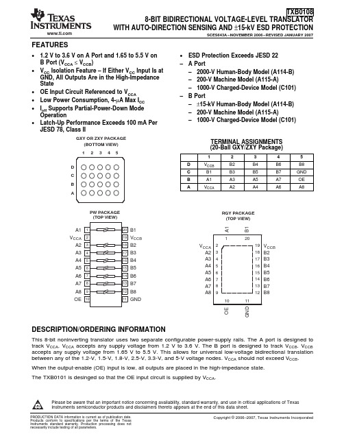
txb0108 8位双向电压电平转换器
Operation
• Latch-Up Performance Exceeds 100 mA Per JESD 78, Class II
To ensure the high-impedance state during power up or power down, OE should be tied to GND through a pulldown resistor; the minimum value of the resistor is determined by the current-sourcing capability of the driver.
Tstg
Supply voltage range
Supply voltage range
Input voltage range(2)
Voltage range applied to any output in the high-impedance or power-off state(2)
Voltage range applied to any output in the high or low state(2)(3)
3vcciisthesupplyvoltageassociatedwiththeinputportcci4submitdocumentationfeedbackwwwticomjanuary2007electricalcharacteristicsoverrecommendedoperatingfreeairtemperaturerangeunlessotherwisenoted12timingrequirementsta25cvcca12vtimingrequirementsoverrecommendedoperatingfreeairtemperaturerangev15v01vunlessotherwisenotedtxb01088bitbidirectionalvoltageleveltranslatorwithautodirectionsensingand15kvesdprotectionsces643anovember2006revisedta25c40cto85ctestparametervccavccbunitconditionsmintypmaxminmax12v11vohaioh20?a14vto36vv04vcca12v09volaiol20?a14vto36vv04vohbioh20?a165vto55vv04ccbvvolbiol20?a165vto55v04viioe12vto36v165vto55v12?aaport0v0vto55v12ioff?abport0vto36v0v12iozaorbportoegnd12vto36v165vto55v12?a12v006165vto55v14vto36v5vivcciorgndicca?aio036v0v20v55v212v34165vto55v14vto36v5vivcciorgndiccb?aio036v0v20v55v212v35vivcciorgndiccaiccb165vto55vio014vto36v?a10vivcciorgnd12v005icczaio0165vto55v14vto36voegnd?a5vivcciorgnd12v33icczbio0165vto55v14vto36voegnd?a5cioe12vto36v165vto55v555pfaportcio12vto36v165vto55vbport8565pf1
10G光模块 安捷伦公司86100D示波器介绍 2010

10Gb/s光电器件测试新挑战Hu HaiyangApplication EngineerAgilent Technologies2010-10-15Standardsand Application Testing? Agilent Technologies, Inc. 2010? Agilent Technologies, Inc. 2010内容安排?10G 光接口模块&测试标准?10G 光接口测试需求及解决方案?10G 光接口测试常见问题?86100D 简介? Agilent Technologies, Inc. 2010光收发模块的发展光接口的优点¨高带宽¨传输距离远¨电气干扰小¨可靠性高¨传输密度大经济性维护性扩展性发展方向复杂性&多样性:多标准智能化:热插拔/具有数字诊断功能高速:>10G 速率模块需求快速稳定增长高密度:并行光器件波长可调: DWDM 应用主要应用?以太网交换机?存储局域网?磁盘阵列/RAID 系统?主机总线适配器?高端服务器和网关?城域网中的路由器10G 光模块将进入稳定成长期? Agilent Technologies, Inc. 2010不同的封装光接口模块CFP LR44x10GQSFP 4x10GSNAP12 12x10G光纤通道: 1G(1x) ⇒2G(2x) ⇒4.25G(4x) ⇒8.5G(8x) ⇒14.2G(16x) ⇒40G?以太网: 1G ⇒10 G, next 25G? 40G? 100G?SFP+? Agilent Technologies, Inc. 2010MSA 多源协议MSA¡s SFP SFP+QSFP Xenpak X2XFP 300 Pin协议光纤通道以太网Sonet/SDH DWDM CWDM选件SR LR ER LRM Extended距离>100m >300m >500m >1km >10km速率(<10G)155Mb 1.0625 Gig 1.25 Gig 2.488Gig 2.5Gig 2.7Gig 3.125Gig 4.25Gig 5Gig 6.25Gig 8.5Gig速率(>10G)9.953 Gig 10.3125 Gig 10.519 Gig 10.709Gig 11.1Gig 11.3Gig? Agilent Technologies, Inc. 2010比较各种封装尺寸10Gb/s 主流产品? Agilent Technologies, Inc. 2009以太网名称如何理解描述(m ):?S: 短波长(850nm, 多模)?L: 长波长(1310nm, 主要是单模, 少量多模)?E: 扩展波长(1550nm, 单模)?T: 双绞线电缆?C: 同轴电缆(铜)?K: 背板描述(n ):?X: 8B/10B 编码?R: 64B/66B 编码?W: STS-192 封装64B/66B 编码(SONET )第2参数:?M 在-LRM 意味着多模?附加在最后的数字表明通道(lanes )数量, 比如-CX4, -LX410G BASE -(m )(n )数据速率基带传输媒质? Agilent Technologies,Inc. 200910GE网络规范?2002, IEEE802.3ae-2002包含7个光纤标准和XAUI 接口::¨10GBASE-LX4:4x3.125Gb/s, CWDM, >300m¨10GBASE-ER, -LR, -SR¨10GBASE-EW, -LW, -SW¨XAUI接口是10G以太网连接MAC 和PHY之间的电口.?2004, 10GBASE-CX4推出(IEEE802.3ak-2004):XAUI信号在同轴电缆传输(15m,4x2.5G Infiniband,预加重)?20069月.¨10GBASE-T 随IEEE802.3an-2006推出. 规范10GE在双绞线铜揽传输.¨10GBASE-LRM 随IEEE802.3aq-2006推出. 10GE在已铺设多模光纤传输?2007, IEEE802.3ap-2007:背板接口标准.¨1000BASE-KX¨1x1.25Gb/s¨10GBASE-KX4¨4x 3.125Gbps¨10GBASE-KR¨1x 10.3125Gbps10GbESwitch CardComputerBlade or LineCard 10G Electrical25G Electrical25G Optical 4 @ 25G Optical40GBASE-KR4? Agilent Technologies, Inc. 2010? Agilent Technologies, Inc. 201010G 光通信应用标准10 G 以太网( ) ¨本地网络(LAN)Overview: /w/index.php?title=10_gigabit_Ethernet&oldid=158488764?802.3ae:10 GbE: 10GBASE-SR, -LR, -ER, -SW, -LW, -EW ?802.3aq:10 Gb/s 多模光纤以太网: 10GBASE-LRM ?802.3ab:40G/100G ?SFP+ 模块被802.3aq 标准采纳光纤通道( ) ¨存储网络(SAN)Overview: /w/index.php?title=Fibre_Channel&oldid=157471662)?FC-PI-5: 物理层10x FC/16x FC ?FC-FS-5: 协议层: 帧和信令标准?其它协议层标准T11.3SFF ( ) ¨小尺寸封装Small Form Factor?SFF-8431: 8.5G & 10G 增强型SFF 即插即用模块¡SFP+¡?SFF-8432: 针对¡SFP+¡机械性能指标?SFF-8083:¡SFP+¡ 一致性板卡边沿连接器? Agilent Technologies, Inc. 2009光纤通道名称如何理解1200-SM -LC -L数据速率1 600 --1 600 MB/s 16xFC 14.02Gb/s 1 200 --1 200 MB/s 10xFC 10.3125Gb/s 800 --800 MB/s 8x FC 8.5gb/s 400 --400 MB/s 4xFC 4.25Gb/s 200 --200 MB/s 2xFC 2.125Gb/s 100 --100 MB/s 1x FC 1.063Gb/s传输媒质SM ¨单模M5 --50¦m 多模(OM2)M5E ¨50¦m 多模(OM3)M5F --50¦m 多模(OM4)M6 --62.5¦m 多模(OM1)SE ¨非平衡电接口DF ¨平衡电接口交互类型SN ¨短波长(850 nm) &限幅接收机SA --短波长(850 nm) &线性接收机LL ¨长波长(1310 nm / 1550 nm) &限幅接收机LC ¨低成本长波长(1310 nm ) &限幅接收机LZ --长波长(1490nm) &限幅接收机LA --长波长(1310 nm / 1550 nm) &线性接收机EL ¨电口&无均衡接收机EA --电口&带均衡接收机距离V ¨超长距离(>50 km)L ¨长距离(>10 km)M ¨中等距离(>4 km)I ¨短距离(>2 km)S ¨超短距离(>70 m)限幅和线性接收机V outP inV outP in? Agilent Technologies, Inc. 2010内容安排?10G 光接口模块&测试标准?10G 光接口测试需求及解决方案?10G 光接口测试常见问题?86100D 简介? Agilent Technologies, Inc. 201010G 光接口测试参数IEEE802.3ae/ab(2008)& FC-PI-5(2010)参数解释SM MM 参数解释SM MM发射机测试CW 中心波长√√接收及测试RMS BW RMS 光谱宽度√SMRR 边模抑制比√BW 20dB 谱宽√P out 平均功率√√OMA 光调制幅度√√Tr/Tf 上升/下降时间√√RIN OMA 相对噪声强度√√P over 过载功率√√ER 消光比√√JT接收抖动容限(OMA)√√TDP 色散代价√P unstress (OMA)接收灵敏度(OMA)√√TJ 总抖动√√RL 回波损耗√√DJ 确定抖动√√F 3dB 3dB 截止频率√√DDPWS 数据相关脉冲宽度收缩√√F 10dB10dB 截止频率√UJ 不相关抖动√√P Stress (OMA)压力眼图灵敏度√VECP 垂直眼图闭合代价√TWDP发射波形色散代价√? Agilent Technologies, Inc. 2010¡抖动分析¡ & ¡幅度分析¡-86100X-200抖动分析选件& 300幅度分析选件?时间噪声(抖动)/幅度噪声→眼图闭合→误码?抖动分析帮助我们探测隐藏在数据上升/下降变化边沿不在预期时间出现背后的机制. 能否采用同样的手段分析信号的幅度电平偏离理想位置??理解什么原因造成眼图闭合可以帮助我们解决问题DeterministicJitter (DJ)RandomJitter (RJ)Data DependentJitter (DDJ)Inter-symbolInterference (ISI)Duty CycleDistortion (DCD)PeriodicJitter PJTotalJitter (TJ)DeterministicInterference( (DI)RandomInterference( (RI)Data DependentInterference(DDI)Inter-symbolInterference (ISI)Periodic Interference( PI)TotalInterference(TI)周期性? Agilent Technologies, Inc. 2010光调制幅度OMAOMA: 光发射机输出信号1电平和0电平的幅度差大多数标准要求特殊的测试码型以测量OMA测试波形/不是眼图典型情况是测量如下的方波码型例如: 11111000001111100000¡.86100X-300 幅度分析选件支持任意码型(自动找到1码序列和0码序列而无论其长度新参数86100C V7.00以上版本直接支持OMA 测试N? Agilent Technologies, Inc. 2010Haiyang HU? Agilent Technologies, Inc. 20102132n+1n ? Agilent Technologies, Inc. 2010(锁定) ? Agilent Technologies, Inc. 2010A0OMAJitter为内眼的高度,垂直眼图VECP = 10* log(OMA/A0)? Agilent Technologies, Inc. 201086100X如何进行压力眼图校准测试?消光比 & 交叉点 眼图模式 码型:PRBS, ERCF ON)TJ (BER 1 e-3), RJ, DCD & ISI 抖动模式 (#200)TJ (BER 1e-2) = TJ (BER 1e-3) ¨ 2* RJ? Agilent Technologies, Inc. 20010OMA 眼图模式 码型:1100 参数: 眼图幅度)A0 (BER 1 e-3) 抖动模式/ 幅度分析 (#300), 参数: 眼张开度光域/电域色散电通道TXASIC RX光通道100 差分的 传输线多模光纤E/O O/E收发模块? Agilent Technologies, Inc. 20010Race conditions cause pulse overlap 走的路径条件不一样造成脉冲重叠预加重色散补偿 ¨ 发射机(Tx)端发射信号没有预加重接收信号N4916B 4-阶预加重转换器3.125 Gb/s发射信号 有预加重6.25 Gb/s12.5 Gb/s接收信号那些应用需要? ?>5Gb/s信号在长电缆 或 PCB中传输需要3- 和 4- 阶预加重? Agilent Technologies, Inc. 20010均衡器色散补偿 ¨ 接收机(Rx)端假设 ? 系统线形 ? 信号劣化主要由于码间干扰 (ISI) ? ISI是确定和可不补偿的经过均衡 均衡之前-86100X -201选件内置线性反馈均衡器算法s(t)TX色散通道r(t)均衡器e(t) 符号解码噪声? Agilent Technologies, Inc. 20010新的测试参数 TWDP发射机波形色散代价? 量化评估接收机眼图的相对闭合Transmitter Waveform Dispersion Penalty¨ 参考理想发射机, 理想通道,接收机噪声高斯分布¨ 代价: 信噪比由于发射机波形失真/通道色散造成的劣化? 由ClariPhy Communications, Inc.提出* for IEEE 802.3aq? 8G 光纤通道和IEEE 802.3ax (其他标准也均采纳) 都采纳这个概念系统功率预算发射机功率 最大通道损耗发射机功率 最大通道损耗TWDPSNR RN 接收机噪声SNR effective RX NoiseSNR RN* MATLAB? scripts for TWDP calculations may contain intellectual property owned by ClariPhy Communications, Inc.? Agilent Technologies, Inc. 2010TWDP 测量-86100X -201选件 外部处理? 码型锁定数据,进行捕获 ? 最高的灵活性 ? 高精度86100C DCA-J-86100X -201选件支持在线TWDP测试DCA-J +内置MATLAB? 标准数据捕获 ? 使用测量方便 ? 实时显示结果? Agilent Technologies, Inc. 20010光模块测量结果RIN 测试一致性眼图模板测试消光比/功率测试抖动分析TWDP 测试? Agilent Technologies, Inc. 2010内容安排? 10G光接口模块&测试标准 ? 10G光接口测试需求及解决方案 ? 10G光接口测试常见问题 ? 86100D简介? Agilent Technologies, Inc. 2010测量示波器带宽问题? 发射机测量结果依赖于示波器带宽¨ 带宽太大: 噪声高, 过冲, 纹波 ¨ 带宽太小: 高码间干扰, 抖动? 通用规则: 参考接收机¨ 定义测试系统的频响 ¨ 典型的4th 阶贝塞尔滤波器=汤姆逊低通滤波响应 ¨ 带宽近似于75% 数据速率? 接收机频响有一定的容限参考接收机? Agilent Technologies, Inc. 2010O/E 转换器放大器 (选件)硬件滤波采样器A/D 转换测量示波器带宽问题示波器带宽的影响不加滤波器适合:? 激光器和驱动设计 ? 光器件故障排查加滤波器适合:? 一致性验证 ? ER & OMA 调节 ? 生产质量控制? Agilent Technologies, Inc. 2010? Agilent Technologies, Inc. 2010-9.00.0 1.0 2.0摘自FC-PI-4¡A.1.2.1.1注意:8.5G 速率信号采用,进? Agilent Technologies, Inc. 2010? Agilent Technologies, Inc. 200108条或者10条等光通道? Agilent Technologies, Inc. 2010? Agilent Technologies, Inc. 20010眼图模板测试问题?标准模板¨单次冲击模板(眼图测量模式)意味着¡失败¡¨通过/失败依赖于事件速率和测量时间?统计模板¨标准: 模板失败<= BER * 采样/UI¨显著提高测试重复性, 降低不确定度?模板富余度¨用户可以在*.msk文件定义/编辑目标(100% 富余度)¨Rev 8.0 to 包括基于误码率的1-shot自动富余度测试XFP HCTBXAUI HCTB? Agilent Technologies, Inc. 2009IEEE 802.3ba 针对40G/100G 以太网Sinx/x 函数频谱? Agilent Technologies, Inc. 2010Page 37? Agilent Technologies, Inc. 2009高级眼图分析(401选件)86100X-200抖动分析软件: 最长分析数据码型<215-1 如何分析更长的数据码型的抖动呢? 86100X-401选件帮助解决这个问题。
安森美三极管详细规格参数表(超全)

Product Datasheet Compliance Status12A02CH ENN7482/D (98.0kB)Pb-free ActiveNEW 15GN01CA15GN01CA/D (48.0kB)Pb-free ActiveNEW 2N2905A2N2905A/D (88.0kB)MIL-PRF-19500ActiveNEW 2N30192N3019/D (85.0kB)MIL-PRF-19500ActiveNEW 2N3019S2N3019S/D (86.0kB)MIL-PRF-19500ActiveNEW 2N37002N3700/D (86.0kB)MIL-PRF-19500ActiveNEW2SA14162SA1416/D (102.0kB)Pb-free ActiveNEW2SA14192SA1419/D (305.0kB)Pb-free ActiveNEW 2SA15932SA1593/D (45.0kB)Pb-free ActiveNEW 2SA17052SA1705/D (40.0kB)Pb-free ActiveNEW 2SA17062SA1706/D (42.0kB)Pb-free ActiveNEW 2SA17072SA1707/D (61.0kB)Pb-free ActiveNEW 2SA17092SA1709/D (49.0kB)Pb-free ActiveNEW 2SA18272SA1827/D (52.0kB)Pb-free ActiveNEW 2SA20122SA2012/D (98.0kB)Pb-free ActiveNEW 2SA20162SA2016/D (57.0kB)Pb-free ActiveNEW 2SA20992SA2099/D (76.0kB)Pb-free ActiveNEW 2SA21122SA2112/D (28.0kB)Pb-free ActiveNEW 2SA21242SA2124/D (91.0kB)Pb-free ActiveNEW2SA21252SA2125/D (59.0kB)Pb-freeHalide free ActiveNEW2SA21262SA2126/D (54.0kB)Pb-free ActiveNEW 2SA21532SA2153/D (35.0kB)Pb-free ActiveNEW 2SA21692SA2169/D (61.0kB)Pb-free ActiveNEW 2SA22022SA2202/D (58.0kB)Pb-free ActiveNEW 2SA22222SA2222/D (69.0kB)Pb-free ActiveNEW 2SB11222SB1122/D (89.0kB)Pb-free ActiveNEW2SB11432SB1143/D (60.0kB)Pb-free ActiveNEW 2SB12012SB1201/D (45.0kB)Pb-free ActiveNEW 2SB12152SB1215/D (60.0kB)Pb-free ActiveNEW 2SB13022SB1302/D (80.0kB)Pb-free ActiveNEW2SC36462SA1416/D (102.0kB)Pb-free ActiveNEW2SC36492SA1419/D (305.0kB)Pb-free ActiveNEW2SC4487ENN3093/D (61.0kB)Pb-free ActiveNEW2SC44882SA1708/D (68.0kB)Pb-free ActiveNEW2SC46142SA1770/D (60.0kB)Pb-free ActiveNEW 2SC47312SC4731/D (52.0kB)Pb-free ActiveNEW 2SC48372SA1855/D (61.0kB)Pb-free ActiveNEW 2SC5226A2SC5226A/D (75.0kB)Pb-free ActiveNEW2SC5227A2SC5227A/D (75.0kB)Pb-free ActiveNEW2SC5231A2SC5231A/D (65.0kB)Pb-free ActiveNEW 2SC5245A2SC5245A/D (58.0kB)Pb-free ActiveNEW 2SC5347A2SC5347A/D (67.0kB)Pb-free ActiveNEW 2SC5415A2SC5415A/D (92.0kB)Pb-free ActiveNEW2SC5488A2SC5488A/D (57.0kB)Pb-freeHalide free ActiveNEW2SC5501A2SC5501A/D (50.0kB)Pb-free ActiveNEW 2SC5551A2SC5551A/D (76.0kB)Pb-free ActiveNEW2SC57062SA2039/D (61.0kB)Pb-freeHalide free ActiveNEW2SC59942SC5994/D (36.0kB)Pb-free ActiveNEW 2SC60172SA2169/D (61.0kB)Pb-free ActiveNEW 2SC60432SC6043/D (30.0kB)Pb-free ActiveNEW 2SC60962SC6096/D (47.0kB)Pb-free ActiveNEW 2SC60972SC6097/D (51.0kB)Pb-free ActiveNEW 2SC61442SC6144/D (68.0kB)Pb-free ActiveNEW2SD12072SB892/D (62.0kB)Pb-free ActiveNEW 2SD16202SD1620/D (85.0kB)Pb-free ActiveNEW2SD16232SB1123/D (99.0kB)Pb-free ActiveNEW 2SD18012SD1801/D (45.0kB)Pb-free ActiveNEW 2SD18052SD1805/D (96.0kB)Pb-free ActiveNEW 2SD18152SB1215/D (60.0kB)Pb-free ActiveNEW 2SD18162SB1216/D (60.0kB)Pb-free ActiveNEW2SD18352SB1229/D (61.0kB)Pb-free ActiveNEW 30A02CH30A02CH/D (28.0kB)Pb-free ActiveNEW 30A02MH30A02MH/D (28.0kB)Pb-free ActiveNEW 30C02CH30C02CH/D (28.0kB)Pb-free ActiveNEW 50A02MH50A02MH/D (29.0kB)Pb-free ActiveNEW 55GN01CA55GN01CA/D (50.0kB)Pb-free ActiveNEWBC807-25W BC807-25W/D (105.0kB)AEC QualifiedPPAP CapablePb-freeHalide free ActiveNEWBC807-40W BC807-25W/D (105.0kB)AEC QualifiedPPAP CapablePb-freeHalide free ActiveNEWBCW66BCW66GLT1/D (110.0kB)Pb-freeHalide freeAEC QualifiedPPAP Capable ActiveNEWCPH3105CPH3105/D (39.0kB)Pb-free ActiveNEW CPH3106CPH3106/D (33.0kB)Pb-free ActiveNEW CPH3109CPH3109/D (55.0kB)Pb-free ActiveNEW CPH3115CPH3115/D (54.0kB)Pb-free ActiveNEW CPH3116CPH3116/D (46.0kB)Pb-free ActiveNEWCPH3121CPH3121/D (65.0kB)Pb-free ActiveNEW CPH3122CPH3122/D (58.0kB)Pb-free ActiveNEW CPH3123CPH3123/D (43.0kB)Pb-free ActiveNEW CPH3140CPH3140/D (37.0kB)Pb-free ActiveNEW CPH3145CPH3145/D (44.0kB)Pb-free ActiveNEW CPH3205CPH3205/D (39.0kB)Pb-free ActiveNEW CPH3209CPH3209/D (55.0kB)Pb-free ActiveNEW CPH3215CPH3215/D (54.0kB)Pb-free ActiveNEW CPH3216CPH3216/D (46.0kB)Pb-free ActiveNEW CPH3223CPH3223/D (43.0kB)Pb-free ActiveNEW CPH3240CPH3240/D (37.0kB)Pb-free ActiveNEW CPH3245CPH3245/D (44.0kB)Pb-free ActiveNEW CPH5504CPH5504/D (49.0kB)Pb-free ActiveNEW CPH5506CPH5506/D (74.0kB)Pb-free ActiveNEW CPH5517CPH5517/D (45.0kB)Pb-free ActiveNEW CPH5524CPH5524/D (72.0kB)Pb-free ActiveNEW CPH6001A CPH6001A/D (63.0kB)Pb-free ActiveNEW CPH6003A CPH6003A/D (58.0kB)Pb-free ActiveNEW CPH6020CPH6020/D (258.0kB)Pb-free ActiveNEWCPH6021ENA1910/D (372.0kB)Pb-freeHalide free ActiveNEWCPH6121CPH6121/D (47.0kB)Pb-free ActiveNEW CPH6122CPH6122/D (48.0kB)Pb-free ActiveNEW CPH6123CPH6123/D (55.0kB)Pb-free ActiveNEW CPH6153CPH6153/D (255.0kB)Pb-free ActiveNEW CPH6223CPH6123/D (55.0kB)Pb-free ActiveNEW CPH6501CPH6501/D (65.0kB)Pb-free ActiveNEWEC3H02BA EC3H02BA/D (283.0kB)Pb-freeHalide free ActiveNEWEC4H09C EC4H09C/D (52.0kB)Pb-freeHalide free ActiveNEWECH8501ECH8501/D (421.0kB)Pb-freeHalide free ActiveNEWMCH3007MCH3007/D (326.0kB)Pb-freeHalide free ActiveNEWMCH4014MCH4014/D (355.0kB)Pb-freeHalide free ActiveNEWMCH4015MCH4015/D (354.0kB)Pb-freeHalide free ActiveNEWMCH4016MCH4016/D (355.0kB)Pb-freeHalide free ActiveNEWMCH4017MCH4017/D (355.0kB)Pb-freeHalide free ActiveNEWMCH4020MCH4020/D (283.0kB)Pb-free ActiveNEW MCH4021MCH4021/D (283.0kB)Pb-free ActiveNEW MCH5541MCH5541/D (48.0kB)Pb-free ActiveNEW MCH6102MCH6102/D (39.0kB)Pb-free ActiveNEW MCH6202MCH6202/D (39.0kB)Pb-free ActiveNEW MCH6541MCH6541/D (65.0kB)Pb-free ActiveNEW MCH6542MCH6542/D (60.0kB)Pb-free ActiveNEW MCH6544MCH6544/D (57.0kB)Pb-free ActiveNEWMCH6545MCH6545/D (52.0kB)Pb-free ActiveNEWMSD1819A-R MSD1819A-RT1/D (209.0kB Pb-free Halide free AEC QualifiedPPAP CapableActiveNEW NSM6056MT1G NSM6056M/D (102.0kB)Pb-freeHalide freeActiveNEW NSM80100M NSM80100M/D (109.0kB)Pb-freeHalide freeActiveNEW NSM80101M NSM80101M/D (108.0kB)Pb-freeHalide freeActiveNEW PCP1103PCP1103/D (266.0kB)Pb-freeHalide freeActiveNEW PCP1203PCP1203/D (267.0kB)Pb-freeHalide free ActiveNEW15C02CH 15C02CH/D (44.0kB)Pb-free Active 2N2907A 2N2907A/D (89.0kB)MIL-PRF-19500Active 2N30552N3055/D (70.0kB)Pb-free Active 2N3055A 2N3055A/D (89.0kB)Pb-free Active 2N34422N3442/D (65.0kB)Pb-free Active 2N37712N3771/D (85.0kB)Pb-free Active 2N37722N3771/D (85.0kB)Pb-free Active 2N37732N3773/D (93.0kB)Pb-free Active 2N39042N3903/D (177.0kB)Pb-free Active 2N39062N3906/D (173.0kB)Pb-free Active 2N41242N4123/D (115.0kB)Pb-free Active 2N44012N4401/D (195.0kB)Pb-free Active 2N44032N4403/D (118.0kB)Pb-freeActive 2N49182N4918/D (117.0kB)Pb-freeHalide freeActive 2N49192N4918/D (117.0kB)Pb-freeHalide freeActive 2N49202N4918/D (117.0kB)Pb-freeHalide freeActive 2N49212N4921/D (90.0kB)Pb-freeHalide freeActive 2N49222N4921/D (90.0kB)Pb-freeHalide freeActive 2N49232N4921/D (90.0kB)Pb-freeHalide free Active 2N50382N5038/D (79.0kB)Pb-free Active 2N50872N5087/D (155.0kB)Pb-free Active 2N50882N5088/D (83.0kB)Pb-free Active 2N50892N5088/D (83.0kB)Pb-freeActive 2N51902N5191/D (84.0kB)Pb-freeHalide freeActive 2N51912N5191/D (84.0kB)Pb-freeHalide freeActive 2N51922N5191/D (84.0kB)Pb-freeHalide freeActive2N51942N5194/D (86.0kB)Pb-freeHalide free Active2N51952N5194/D (86.0kB)Pb-freeHalide free Active2N53022N5302/D (92.0kB)Pb-free Active 2N54012N5401/D (145.0kB)Pb-free Active 2N55502N5550/D (88.0kB)Pb-free Active 2N55512N5550/D (88.0kB)Pb-free Active2N56552N5655/D (80.0kB)Pb-freeHalide free Active2N56572N5655/D (80.0kB)Pb-freeHalide free Active2N56842N5684/D (114.0kB)Pb-free Active 2N56862N5684/D (114.0kB)Pb-free Active 2N58832N5883/D (94.0kB)Pb-free Active 2N58842N5883/D (94.0kB)Pb-free Active 2N58852N5883/D (94.0kB)Pb-free Active 2N58862N5883/D (94.0kB)Pb-free Active 2N61072N6107/D (90.0kB)Pb-free Active 2N61092N6107/D (90.0kB)Pb-free Active 2N61112N6107/D (90.0kB)Pb-free Active 2N62882N6107/D (90.0kB)Pb-free Active 2N62922N6107/D (90.0kB)Pb-free Active 2N63382N6338/D (135.0kB)Pb-free Active 2N63412N6338/D (135.0kB)Pb-free Active 2N64872N6487/D (92.0kB)Pb-free Active 2N64882N6487/D (92.0kB)Pb-free Active 2N64902N6487/D (92.0kB)Pb-free Active 2N64912N6487/D (92.0kB)Pb-free Active 2N65202N6515/D (116.0kB)Pb-free Active 2SA10202SA1020/D (93.0kB)Pb-free Active 2SA14172SA1417/D (57.0kB)Pb-free Active 2SA17082SA1708/D (68.0kB)Pb-free Active 2SA17702SA1770/D (60.0kB)Pb-free Active2SA17742SA1774/D (53.0kB)Pb-freeHalide free Active2SA20132SA2013/D (57.0kB)Pb-free Active2SA2029M32SA2029M3/D (45.0kB)Pb-freeHalide free Active2SA20392SA2039/D (61.0kB)Pb-free Active 2SB11232SB1123/D (99.0kB)Pb-free Active 2SB11242SB1124/D (44.0kB)Pb-free Active2SB12022SB1202/D (58.0kB)Pb-free Active 2SB12042SB1204/D (103.0kB)Pb-free Active2SB12052SB1205/D (50.0kB)Pb-free Active2SC33322SA1319/D (59.0kB)Pb-free Active2SC36472SA1417/D (57.0kB)Pb-free Active 2SC36482SA1418/D (96.0kB)Pb-free Active2SC46172SC4617/D (45.0kB)Pb-freeHalide free Active2SC55662SA2013/D (57.0kB)Pb-free Active 2SC55692SA2016/D (57.0kB)Pb-free Active2SC5658M3T5G2SC5658M3/D (125.0kB)Pb-freeHalide free Active2SC5658RM3T5G2SC5658M3/D (125.0kB)Pb-freeHalide free Active2SC57072SA2040/D (58.0kB)Pb-free Active 2SC58882SA2099/D (76.0kB)Pb-free Active 2SC59642SA2125/D (59.0kB)Pb-free Active 2SC60822SC6082/D (52.0kB)Pb-free Active 2SC60942SC6094/D (49.0kB)Pb-free Active 2SC60952SC6095/D (49.0kB)Pb-free Active 2SD16242SD1624/D (44.0kB)Pb-free Active 2SD16852SD1685/D (113.0kB)Pb-free Active 2SD18022SB1202/D (58.0kB)Pb-free Active BC237B BC237/D (59.0kB)Pb-free Active BC307B BC307/D (87.0kB)Pb-free Active BC327BC327/D (102.0kB)Pb-free Active BC327-025BC327/D (102.0kB)Pb-free Active BC327-25BC327/D (102.0kB)Pb-free Active BC337BC337/D (141.0kB)Pb-free Active BC337-025BC337/D (141.0kB)Pb-free Active BC337-040BC337/D (141.0kB)Pb-free Active BC337-25BC337/D (141.0kB)Pb-free Active BC337-40BC337/D (141.0kB)Pb-free Active BC369BC368/D (60.0kB)Pb-free Active BC490BC490/D (78.0kB)Pb-free Active BC546B BC546/D (72.0kB)Pb-free Active BC547B BC546/D (72.0kB)Pb-free Active BC547C BC546/D (72.0kB)Pb-free Active BC548B BC546/D (72.0kB)Pb-free Active BC548C BC546/D (72.0kB)Pb-free Active BC549C BC549B/D (53.0kB)Pb-free Active BC550C BC550C/D (59.0kB)Pb-free Active BC556B BC556B/D (81.0kB)Pb-free Active BC557B BC556B/D (81.0kB)Pb-free Active BC557C BC556B/D (81.0kB)Pb-free Active BC558B BC556B/D (81.0kB)Pb-free Active BC560C BC560C/D (131.0kB)Pb-free Active BC637BC635/D (92.0kB)Pb-free Active BC639BC635/D (92.0kB)Pb-free Active BC640BC640/D (88.0kB)Pb-free ActiveBC807-16L BC807-16LT1/D (118.0kB)Pb-freeHalide freeActive BC807-25L BC807-16LT1/D (118.0kB)Pb-freeHalide freeActive BC807-40L BC807-16LT1/D (118.0kB)Pb-freeHalide freeActive BC808BC808-25LT1/D (128.0kB)Pb-freeHalide freeActive BC817-16L BC817-16LT1/D (119.0kB)Pb-freeHalide freeActive BC817-25L BC817-16LT1/D (119.0kB)Pb-freeHalide freeActive BC817-40L BC817-16LT1/D (119.0kB)Pb-freeHalide freeActive BC818BC818-40LT/D (128.0kB)Pb-freeHalide freeActive BC846AL BC846ALT1/D (131.0kB)Pb-freeHalide freeActive BC846B BC846BDW1T1/D (127.0kB Pb-freeHalide freeActive BC846BL BC846ALT1/D (131.0kB)Pb-freeHalide freeActive BC846BM3T5G BC846BM3/D (87.0kB)Pb-freeHalide freeActive BC846BPDW1BC846BPDW1T1/D (166.0k Pb-freeHalide freeActive BC846BW BC846AWT1/D (128.0kB)Pb-freeHalide freeActive BC846C BC846BDW1T1/D (127.0kB Pb-freeHalide freeActive BC847AL BC846ALT1/D (131.0kB)Pb-freeHalide freeActive BC847AW BC846AWT1/D (128.0kB)Pb-freeHalide freeActive BC847BDW1BC846BDW1T1/D (127.0kB Pb-freeHalide freeActive BC847BL BC846ALT1/D (131.0kB)Pb-freeHalide freeActive BC847BP BC846BPDW1T1/D (166.0k Pb-freeHalide freeActive BC847BPDXV6BC847BPDXV6T1/D (76.0kB Pb-freeHalide freeActive BC847BT BC847ATT1/D (71.0kB)Pb-freeHalide freeActive BC847BW BC846AWT1/D (128.0kB)Pb-freeHalide freeActive BC847CDXV6BC847CDXV6T1/D (96.0kB)Pb-freeHalide freeActiveBC847CL BC846ALT1/D (131.0kB)AEC Qualified PPAP Capable Pb-freeHalide freeActive BC847CT BC847ATT1/D (71.0kB)Pb-freeHalide freeActive BC847CW BC846AWT1/D (128.0kB)Pb-freeHalide freeActive BC848AL BC846ALT1/D (131.0kB)Pb-freeHalide freeActive BC848BL BC846ALT1/D (131.0kB)Pb-freeHalide freeActive BC848BW BC846AWT1/D (128.0kB)Pb-freeHalide freeActive BC848CDW1BC846BDW1T1/D (127.0kB Pb-freeHalide freeActive BC848CL BC846ALT1/D (131.0kB)Pb-freeHalide freeActive BC848CPD BC846BPDW1T1/D (166.0k Pb-freeHalide freeActive BC848CW BC846AWT1/D (128.0kB)Pb-freeHalide freeActive BC849BL BC846ALT1/D (131.0kB)Pb-freeHalide freeActive BC849CL BC846ALT1/D (131.0kB)Pb-freeHalide freeActive BC850BL BC846ALT1/D (131.0kB)Pb-freeHalide freeActive BC850CL BC846ALT1/D (131.0kB)Pb-freeHalide freeActive BC856 SERIES BC856BM3/D (55.0kB)Pb-freeHalide freeActive BC856AL BC856ALT1/D (167.0kB)Pb-freeHalide freeActive BC856B BC856BDW1T1/D (172.0kB Pb-freeHalide freeActive BC856BL BC856ALT1/D (167.0kB)Pb-freeHalide freeActive BC856BW BC856BWT1/D (143.0kB)Pb-freeHalide freeActive BC857AL BC856ALT1/D (167.0kB)Pb-freeHalide freeActive BC857BDW1BC856BDW1T1/D (172.0kB Pb-freeHalide freeActive BC857BL BC856ALT1/D (167.0kB)Pb-freeHalide freeActive BC857BT BC857BTT1/D (74.0kB)Pb-freeHalide freeActive BC857BWBC856BWT1/D (143.0kB)Pb-freeHalide freeActiveBC857CDW1BC856BDW1T1/D (172.0kB Pb-freeHalide freeActive BC857CL BC856ALT1/D (167.0kB)Pb-freeHalide freeActive BC857CW BC856BWT1/D (143.0kB)Pb-freeHalide freeActive BC858AL BC856ALT1/D (167.0kB)Pb-freeHalide freeActive BC858AW BC856BWT1/D (143.0kB)Pb-freeHalide freeActive BC858BL BC856ALT1/D (167.0kB)Pb-freeHalide freeActive BC858BW BC856BWT1/D (143.0kB)Pb-freeHalide freeActive BC858CDXV6BC858CDXV6T1/D (56.0kB)Pb-freeHalide freeActive BC858CLBC856ALT1/D (167.0kB)Pb-freeHalide freeActiveBCP53BCP53T1/D (101.0kB)Pb-free Halide freeActiveBCP56BCP56T1/D (104.0kB)Pb-freeHalide freeActive BCP68BCP68T1/D (128.0kB)Pb-freeHalide freeActive BCP69BCP69T1/D (96.0kB)Pb-freeHalide freeActive BCW30L BCW30LT1/D (240.0kB)Pb-freeHalide freeActive BCW32L BCW32LT1/D (192.0kB)Pb-freeHalide freeActive BCW33L BCW33LT1/D (257.0kB)Pb-freeHalide freeActive BCW65AL BCW65ALT1/D (110.0kB)Pb-freeHalide freeActive BCW68GL BCW68GLT1/D (108.0kB)Pb-freeHalide freeActive BCW70L BCW70LT1/D (265.0kB)Pb-freeHalide freeActive BCW72L BCW72LT1/D (277.0kB)Pb-freeHalide freeActive BCX17L BCX17LT1/D (92.0kB)Pb-freeHalide freeActive BCX19L BCX17LT1/D (92.0kB)Pb-freeHalide freeActive BD135BD135/D (37.0kB)Pb-freeHalide freeActive BD136BD136/D (37.0kB)Pb-freeHalide freeActiveBD137BD135/D (37.0kB)Pb-freeHalide free ActiveBD138BD136/D (37.0kB)Pb-freeHalide free ActiveBD139BD135/D (37.0kB)Pb-freeHalide free ActiveBD140BD136/D (37.0kB)Pb-freeHalide free ActiveBD159BD159/D (56.0kB)Pb-freeHalide free ActiveBD179BD179/D (80.0kB)Pb-freeHalide free ActiveBD180BD180/D (62.0kB)Pb-freeHalide free ActiveBD234BD237/D (63.0kB)Pb-freeHalide free ActiveBD237BD237/D (63.0kB)Pb-freeHalide free ActiveBD241C BD241C/D (93.0kB)Pb-free Active BD242B BD241C/D (93.0kB)Pb-free Active BD242C BD241C/D (93.0kB)Pb-free Active BD243C BD243B/D (91.0kB)Pb-free Active BD244B BD243B/D (91.0kB)Pb-free Active BD244C BD243B/D (91.0kB)Pb-free ActiveBD435BD437/D (59.0kB)Pb-freeHalide free ActiveBD436BD438/D (58.0kB)Pb-freeHalide free ActiveBD437BD437/D (59.0kB)Pb-freeHalide free ActiveBD438BD438/D (58.0kB)Pb-freeHalide free ActiveBD439BD437/D (59.0kB)Pb-freeHalide free ActiveBD440BD438/D (58.0kB)Pb-freeHalide free ActiveBD441BD437/D (59.0kB)Pb-freeHalide free ActiveBD442BD438/D (58.0kB)Pb-freeHalide free ActiveBD787BD787/D (78.0kB)Pb-freeHalide free ActiveBD788BD787/D (78.0kB)Pb-freeHalide free ActiveBD809BD809/D (80.0kB)Pb-free Active BD810BD809/D (80.0kB)Pb-free Active BF422BF422/D (98.0kB)Pb-free Active BF423BF421/D (105.0kB)Pb-free Active BF493S BF493S/D (58.0kB)Pb-free ActiveBF720BF720T1/D (128.0kB)Pb-freeHalide free ActiveBF721BF721T1/D (127.0kB)Pb-freeHalide freeActive BSP16BSP16T1/D (112.0kB)Pb-freeHalide freeActive BSP19A BSP19AT1/D (181.0kB)Pb-freeHalide freeActive BSS63L BSS63LT1/D (111.0kB)Pb-freeHalide freeActive BSS64L BSS64LT1/D (108.0kB)Pb-freeHalide freeActive BSV52L BSV52LT1/D (108.0kB)Pb-freeHalide free ActiveBU406BU406/D (121.0kB)Pb-freeActive BUD42D BUD42D/D (178.0kB)Pb-freeHalide free Active BUH100BUH100/D (246.0kB)Pb-free Active BUH150BUH150/D (238.0kB)Pb-free Active BUH50BUH50/D (247.0kB)Pb-free Active BUL45BUL45/D (205.0kB)Pb-free Active BUL45D2BUL45D2/D (231.0kB)Pb-free Active BUV21BUV21/D (70.0kB)Pb-free Active BUV22BUV22/D (70.0kB)Pb-free Active BUV26BUV26/D (85.0kB)Pb-free Active BUV27BUV27/D (52.0kB)Pb-free Active BUX85BUX85/D (128.0kB)Pb-free Active CPH6531CPH6531/D (59.0kB)Pb-free Active CPH6532CPH6532/D (48.0kB)Pb-free Active D44H11D44H/D (81.0kB)Pb-free Active D44H8D44H/D (81.0kB)Pb-free Active D44VH D44VH/D (84.0kB)Pb-free Active D45C D45C12/D (73.0kB)Pb-free Active D45H11D44H/D (81.0kB)Pb-free Active D45H8D44H/D (81.0kB)Pb-free Active D45VH D44VH/D (84.0kB)Pb-freeActive EMT SERIES EMT1DXV6T1/D (51.0kB)Pb-freeHalide freeActive EMX1EMX1DXV6T1/D (51.0kB)Pb-freeHalide freeActive EMX2DXV6EMX2DXV6T5/D (121.0kB)Pb-freeHalide freeActive EMZ1EMZ1DXV6/D (59.0kB)Pb-freeHalide free Active FH102A FH102A/D (64.0kB)Pb-freeActive HN1B01FDW1HN1B01FDW1T1/D (52.0kB Pb-freeHalide freeActive MBT2222ADW1T1MBT2222ADW1T1/D (164.0Pb-freeHalide freeActive MBT3904DW1MBT3904DW1T1/D (131.0kB Pb-freeHalide freeActive MBT3906DW1MBT3906DW1T1/D (178.0kB Pb-freeHalide freeActiveMBT3946DW1T1MBT3946DW1T1/D (241.0kB Pb-freeHalide freeActive MBT6429DW1MBT6429DW1T1/D (219.0kB Pb-freeHalide freeActive MCH4009MCH4009/D (66.0kB)Pb-freeHalide free ActiveMCH6001MCH6001/D (251.0kB)Pb-free Active MJ14002MJ14001/D (90.0kB)Pb-free Active MJ29552N3055/D (70.0kB)Pb-free Active MJ4502MJ4502/D (128.0kB)Pb-free Active MJ802MJ802/D (70.0kB)Pb-freeActive MJB41C MJB41C/D (84.0kB)Pb-freeHalide freeActive MJB42C MJB41C/D (84.0kB)Pb-freeHalide freeActive MJB44H11MJB44H11/D (64.0kB)Pb-freeHalide freeActive MJB45H11MJB44H11/D (64.0kB)Pb-freeHalide freeActive MJD148MJD148/D (109.0kB)Pb-freeHalide freeActive MJD200MJD200/D (132.0kB)Pb-freeHalide freeActive MJD210MJD200/D (132.0kB)Pb-freeHalide freeActive MJD243MJD243/D (143.0kB)Pb-freeHalide freeActive MJD253MJD243/D (143.0kB)Pb-freeHalide freeActive MJD2955MJD2955/D (117.0kB)Pb-freeHalide freeActive MJD3055MJD2955/D (117.0kB)Pb-freeHalide freeActive MJD31MJD31/D (129.0kB)Pb-freeHalide freeActive MJD31C MJD31/D (129.0kB)Pb-freeHalide freeActive MJD32MJD31/D (129.0kB)Pb-freeHalide freeActive MJD32C MJD31/D (129.0kB)Pb-freeHalide freeActive MJD340MJD340/D (120.0kB)Pb-freeHalide freeActive MJD350MJD340/D (120.0kB)Pb-freeHalide freeActive MJD41C MJD41C/D (117.0kB)Pb-freeHalide freeActive MJD42C MJD41C/D (117.0kB)Pb-freeHalide freeActive MJD44E3MJD44E3/D (89.0kB)Pb-freeHalide freeActiveMJD44H11MJD44H11/D (108.0kB)Pb-freeHalide free ActiveMJD45H11MJD44H11/D (108.0kB)Pb-freeHalide free ActiveMJD47MJD47/D (110.0kB)Pb-freeHalide free ActiveMJD50MJD47/D (110.0kB)Pb-freeHalide free ActiveMJD5731MJD5731/D (114.0kB)Pb-freeHalide free ActiveMJE13003MJE13003/D (107.0kB)Pb-freeHalide free ActiveMJE13005MJE13005/D (150.0kB)Pb-free Active MJE13007MJE13007/D (194.0kB)Pb-free Active MJE13009MJE13009/D (189.0kB)Pb-free Active MJE15033MJE15032/D (75.0kB)Pb-free ActiveMJE171MJE171/D (82.0kB)Pb-freeHalide free ActiveMJE172MJE171/D (82.0kB)Pb-freeHalide free ActiveMJE18004MJE18004/D (225.0kB)Pb-free Active MJE18008MJE18008/D (229.0kB)Pb-free ActiveMJE181MJE171/D (82.0kB)Pb-freeHalide free ActiveMJE182MJE171/D (82.0kB)Pb-freeHalide free ActiveMJE200MJE200/D (115.0kB)Pb-freeHalide free ActiveMJE210MJE200/D (115.0kB)Pb-freeHalide free ActiveMJE243MJE243/D (187.0kB)Pb-freeHalide free ActiveMJE253MJE243/D (187.0kB)Pb-freeHalide free ActiveMJE2955T MJE2955T/D (138.0kB)Pb-free Active MJE3055T MJE2955T/D (138.0kB)Pb-free ActiveMJE340MJE340/D (67.0kB)Pb-freeHalide free ActiveMJE3439MJE3439/D (54.0kB)Pb-freeHalide free ActiveMJE344MJE344/D (62.0kB)Pb-freeHalide free ActiveMJE350MJE350/D (133.0kB)Pb-freeHalide free ActiveMJE371MJE371/D (61.0kB)Pb-freeHalide free ActiveMJE4343MJE4343/D (142.0kB)Pb-free Active MJE5730MJE5730/D (76.0kB)Pb-free Active MJE5731MJE5730/D (76.0kB)Pb-free Active MJE5731A MJE5730/D (76.0kB)Pb-free Active MJE5850MJE5850/D (104.0kB)Pb-free ActiveMJE5851MJE5850/D (104.0kB)Pb-free Active MJE5852MJE5850/D (104.0kB)Pb-free Active MJF15030MJF15030/D (134.0kB)Pb-free Active MJF15031MJF15030/D (134.0kB)Pb-free Active MJF18004MJE18004/D (225.0kB)Pb-free Active MJF18008MJE18008/D (229.0kB)Pb-free Active MJF2955MJF3055/D (115.0kB)Pb-free Active MJF3055MJF3055/D (115.0kB)Pb-free Active MJF31C MJF31C/D (122.0kB)Pb-free Active MJF32C MJF31C/D (122.0kB)Pb-free Active MJF44H11MJF44H11/D (151.0kB)Pb-free Active MJF45H11MJF44H11/D (151.0kB)Pb-free Active MJF47MJF47/D (130.0kB)Pb-free Active MJW18020MJW18020/D (131.0kB)Pb-free Active MMBT2131MMBT2131T1/D (60.0kB)Pb-freeHalide freeActive MMBT2222AL MMBT2222LT1/D (126.0kB)Pb-freeHalide freeActive MMBT2222AM3MMBT2222AM3/D (168.0kB Pb-freeHalide freeActive MMBT2222AT MMBT2222ATT1/D (114.0kB Pb-freeHalide freeActive MMBT2222AW MMBT2222AWT1/D (121.0k Pb-freeHalide freeActive MMBT2222L MMBT2222LT1/D (126.0kB)Pb-freeHalide freeActive MMBT2369AL MMBT2369LT1/D (190.0kB)Pb-freeHalide freeActive MMBT2369L MMBT2369LT1/D (190.0kB)Pb-freeHalide freeActive MMBT2484L MMBT2484LT1/D (191.0kB)Pb-freeHalide freeActive MMBT2907AL MMBT2907ALT1/D (114.0kB Pb-freeHalide freeActive MMBT2907AM3T5G MMBT2907AM3/D (167.0kB Pb-freeHalide freeActive MMBT2907AW MMBT2907AWT1/D (83.0kB Pb-freeHalide freeActive MMBT3416L MMBT3416LT3/D (230.0kB)Pb-freeHalide freeActive MMBT3904L MMBT3904LT1/D (114.0kB)Pb-freeHalide freeActiveMMBT3904T MMBT3904TT1/D (102.0kB)Pb-free Halide free AEC QualifiedPPAP CapableActive MMBT3904W MMBT3904WT1/D (160.0kB Pb-freeHalide freeActive MMBT3906L MMBT3906LT1/D (120.0kB)Pb-freeHalide freeActiveMMBT3906T MMBT3906TT1/D (86.0kB)Pb-freeHalide freeActive MMBT3906W MMBT3904WT1/D (160.0kB Pb-freeHalide freeActive MMBT4124MMBT4124LT1/D (144.0kB)Pb-freeHalide freeActive MMBT4126LT1MMBT4126LT1/D (154.0kB)Pb-freeHalide freeActive MMBT4401L MMBT4401LT1/D (155.0kB)Pb-freeHalide freeActive MMBT4401M3T5G MMBT4401M3/D (125.0kB)Pb-freeHalide freeActive MMBT4401WT1MMBT4401WT1/D (180.0kB Pb-freeHalide freeActive MMBT4403L MMBT4403LT1/D (151.0kB)Pb-freeHalide freeActive MMBT4403M3T5G MMBT4403M3/D (125.0kB)Pb-freeHalide freeActive MMBT4403W MMBT4403WT1/D (178.0kB Pb-freeHalide freeActive MMBT489MMBT489LT1/D (121.0kB)Pb-freeHalide freeActive MMBT5087L MMBT5087LT1/D (231.0kB)Pb-freeHalide freeActive MMBT5088L MMBT5088LT1/D (192.0kB)Pb-freeHalide freeActive MMBT5089L MMBT5088LT1/D (192.0kB)Pb-freeHalide freeActive MMBT5401L MMBT5401LT1/D (115.0kB)Pb-freeHalide freeActive MMBT5550L MMBT5550LT1/D (121.0kB)Pb-freeHalide freeActive MMBT5551L MMBT5550LT1/D (121.0kB)Pb-freeHalide freeActive MMBT5551M3T5G MMBT5551M3/D (151.0kB)Pb-freeHalide freeActive MMBT6428L MMBT6428LT1/D (194.0kB)Pb-freeHalide freeActive MMBT6429L MMBT6428LT1/D (194.0kB)Pb-freeHalide freeActive MMBT6517L MMBT6517LT1/D (176.0kB)Pb-freeHalide freeActive MMBT6520L MMBT6520LT1/D (116.0kB)Pb-freeHalide freeActive MMBT6521L MMBT6521LT1/D (289.0kB)Pb-freeHalide freeActive MMBT8099L MMBT8099LT1/D (158.0kB)Pb-freeHalide freeActive MMBT918LMMBT918LT1/D (113.0kB)Pb-freeHalide freeActiveMMBTA05L MMBTA05LT1/D (103.0kB)Pb-freeHalide freeActive MMBTA06L MMBTA05LT1/D (103.0kB)Pb-freeHalide freeActive MMBTA06WT1MMBTA06WT1/D (133.0kB)Pb-freeHalide freeActive MMBTA42L MMBTA42LT1/D (89.0kB)Pb-freeHalide freeActive MMBTA55L MMBTA55LT1/D (103.0kB)Pb-freeHalide freeActive MMBTA56L MMBTA55LT1/D (103.0kB)Pb-freeHalide freeActive MMBTA56W MMBTA56WT1/D (132.0kB)Pb-freeHalide freeActive MMBTA70L MMBTA70LT1/D (240.0kB)Pb-freeHalide freeActive MMBTA92L MMBTA92LT1/D (105.0kB)Pb-freeHalide freeActive MMBTH10L MMBTH10LT1/D (123.0kB)Pb-freeHalide freeActive MMBTH10M3T5G MMBTH10M3/D (119.0kB)Pb-freeHalide freeActive MMJT350T1MMJT350T1/D (102.0kB)Pb-freeHalide free ActiveMPS2222MPS2222/D (90.0kB)Pb-free Active MPS2222A MPS2222/D (90.0kB)Pb-free Active MPS2907A MPS2907A/D (129.0kB)Pb-free Active MPS4124MPS4124/D (48.0kB)Pb-free Active MPS4250MPS4250/D (86.0kB)Pb-free Active MPS5172MPS5172/D (98.0kB)Pb-free Active MPS650MPS650/D (68.0kB)Pb-free Active MPS651MPS650/D (68.0kB)Pb-free Active MPS6652MPS6601/D (86.0kB)Pb-free Active MPS6726MPS6726/D (93.0kB)Pb-free Active MPS750MPS650/D (68.0kB)Pb-free Active MPS751MPS650/D (68.0kB)Pb-free Active MPS8099MPS8099/D (122.0kB)Pb-free Active MPSA05MPSA05/D (89.0kB)Pb-free Active MPSA06MPSA05/D (89.0kB)Pb-free Active MPSA18MPSA18/D (79.0kB)Pb-free Active MPSA42MPSA42/D (102.0kB)Pb-free Active MPSA44MPSA44/D (66.0kB)Pb-free Active MPSA55MPSA05/D (89.0kB)Pb-free Active MPSA56MPSA05/D (89.0kB)Pb-free Active MPSA92MPSA92/D (104.0kB)Pb-free Active MPSH10MPSH10/D (82.0kB)Pb-free Active MPSW01MPSW01/D (95.0kB)Pb-free Active MPSW01A MPSW01/D (95.0kB)Pb-free Active MPSW05MPSW05/D (96.0kB)Pb-free Active MPSW06MPSW05/D (96.0kB)Pb-free Active MPSW42MPSW42/D (96.0kB)Pb-freeActiveMPSW51MPSW51/D (96.0kB)Pb-free ActiveMPSW55MPSW55/D (97.0kB)Pb-free Active MPSW56MPSW55/D (97.0kB)Pb-free Active MPSW92MPSW92/D (98.0kB)Pb-free Active MSA1162MSA1162GT1/D (41.0kB)Pb-freeHalide freeActive MSB1218A-RT1MSB1218A-RT1/D (117.0kB Pb-freeHalide freeActive MSB709-RT1MSB709-RT1/D (42.0kB)Pb-freeHalide freeActive MSB92MSB92T1G/D (73.0kB)Pb-freeHalide freeActive MSB92A MSB92ASWT1/D (85.0kB)Pb-freeHalide freeActive MSB92AW MSB92WT1/D (117.0kB)Pb-freeHalide freeActive MSB92W MSB92WT1/D (117.0kB)Pb-freeHalide freeActive MSC2712GT1MSC2712GT1/D (31.0kB)Pb-freeHalide freeActive MSD1328-RT1MSD1328-RT1/D (30.0kB)Pb-freeHalide freeActive MSD42SW MSD42SWT1/D (102.0kB)Pb-freeHalide freeActive MSD42W MSD42WT1/D (125.0kB)Pb-freeHalide freeActive MSD601-R MSD601-RT1/D (42.0kB)Pb-freeHalide freeActive MSD602-RT1MSD602-RT1/D (42.0kB)Pb-freeHalide freeActive NJD1718NJD1718/D (100.0kB)Pb-freeHalide freeActive NJD2873NJD2873T4/D (93.0kB)Pb-freeHalide freeActive NJT4030P NJT4030P/D (274.0kB)Pb-freeHalide freeActive NJT4031NT1G NJT4031N/D (104.0kB)Pb-freeHalide free Active NJW0302NJW0281/D (74.0kB)Pb-free Active NJW1302NJW3281/D (83.0kB)Pb-free Active NJW21194NJW21193/D (90.0kB)Pb-freeActive NJX1675P NJX1675P/D (380.0kB)Pb-freeHalide freeActive NS2029M3NS2029M3/D (69.0kB)Pb-freeHalide freeActive NSS1C200NSS1C200MZ4/D (100.0kB)Pb-freeHalide freeActive NSS40300NSS40300MZ4/D (109.0kB)Pb-freeHalide freeActive。
MAX1448EHJ+T中文资料
D E C
10
OUTPUT DRIVERS
D9–D0
PD
REF
REFSYSTEM+ BIAS
OVDD OGND
REFOUT REFIN REFP
COM REFN
OE
Pin Configuration appears at end_______________________________________________________ Maxim Integrated Products
元器件交易网
10-Bit, 80Msps, Single 3.0V, Low-Power ADC with Internal Reference MAX1448
ABSOLUTE MAXIMUM RATINGS
VDD, OVDD to GND ...............................................-0.3V to +3.6V OGND to GND.......................................................-0.3V to +0.3V IN+, IN- to GND........................................................-0.3V to VDD REFIN, REFOUT, REFP, REFN, and COM to GND..........................-0.3V to (VDD + 0.3V) OE, PD, CLK to GND..................................-0.3V to (VDD + 0.3V) D9–D0 to GND.........................................-0.3V to (OVDD + 0.3V) Continuous Power Dissipation (TA = +70°C) 32-Pin TQFP (derate 18.7mW/°C above +70°C)......1495.3mW Operating Temperature Range ...........................-40°C to +85°C Junction Temperature ......................................................+150°C Storage Temperature Range ............................-60°C to +150°C Lead Temperature (soldering, 10s) .................................+300°C
电子信息工程、通信工程、电气类等专业面试将会遇到试题大全
电子信息工程、通信工程、电气类等专业面试将会遇到试题大全模拟电路1、基尔霍夫定理的内容是什么?(仕兰微电子)基尔霍夫电流定律是一个电荷守恒定律,即在一个电路中流入一个节点的电荷与流出同一个节点的电荷相等。
基尔霍夫电压定律是一个能量守恒定律,即在一个回路中回路电压之和为零.2、平板电容公式(C=εS/4πkd)。
(未知)3、最基本的如三极管曲线特性。
(未知)4、描述反馈电路的概念,列举他们的应用。
(仕兰微电子)5、负反馈种类(电压并联反馈,电流串联反馈,电压串联反馈和电流并联反馈);负反馈的优点(降低放大器的增益灵敏度,改变输入电阻和输出电阻,改善放大器的线性和非线性失真,有效地扩展放大器的通频带,自动调节作用)(未知)6、放大电路的频率补偿的目的是什么,有哪些方法?(仕兰微电子)7、频率响应,如:怎么才算是稳定的,如何改变频响曲线的几个方法。
(未知)8、给出一个查分运放,如何相位补偿,并画补偿后的波特图。
(凹凸)9、基本放大电路种类(电压放大器,电流放大器,互导放大器和互阻放大器),优缺点,特别是广泛采用差分结构的原因。
(未知)10、给出一差分电路,告诉其输出电压Y+和Y-,求共模分量和差模分量。
(未知)11、画差放的两个输入管.(凹凸)12、画出由运放构成加法、减法、微分、积分运算的电路原理图。
并画出一个晶体管级的运放电路。
(仕兰微电子)13、用运算放大器组成一个10倍的放大器.(未知)14、给出一个简单电路,让你分析输出电压的特性(就是个积分电路),并求输出端某点的 rise/fall时间。
(Infineon笔试试题)15、电阻R和电容C串联,输入电压为R和C之间的电压,输出电压分别为C上电压和R上电压,要求制这两种电路输入电压的频谱,判断这两种电路何为高通滤波器,何为低通滤波器。
当RC〈< period —setup ?hold16、时钟周期为T,触发器D1的建立时间最大为T1max,最小为T1min。
HCPL-3150中文资料
N/C 1 ANODE 2 CATHODE 3
SHIELD
16 VCC 15 VO 14 VEE
CATHODE 3
N/C 4
SHIELD HCPL-3150
TRUTH TABLE
6 VO 5 VEE
ANODE 6 CATHODE 7
N/C 8
SHIELD HCPL-315J
11 VCC 10 VO 9 VEE
10 kV/µs
Yes
No
No
Widebody (400 mil) HCNW-3120
1
VIORM 1414 Vpeak
5000 Vrms/1min.
2A
Small Outline SO-16
HCPL-315J HCPL-316J HCPL-314J
2
1
2
0.5A
VIORM 891 Vpeak
3750 Vrms/1 min.
Standard DIP Package
9.40 (0.370) 9.90 (0.390)
87
6
A 3150 Z YYWW
PIN ONE 1
2
3
1.19 (0.047) MAX.
5 OPTION CODE* DATE CODE
6.10 (0.240) 6.60 (0.260)
7.36 (0.290) 7.88 (0.310)
2A
0.4A
15 kV/µs
10 kV/µs
Yes
No
Yes
No
Ordering Information
Specify Part Number followed by Option Number (if desired)
T018MMSP001K1_1_3D_TSMC0.18um工艺介绍
T018MMSP001K1_1_3D_TSMC0.18um⼯艺介绍Ver. Eff_Date ECN No. Author Change Description1.3D 01-10-06 E030200601061 C. W. Hung 1.Add(1)New devices : rnhpoly_dis, rnlpoly_dis,rphpoly_dis, rphripoly_dis, rplpoly_dis for3 terminal poly resistors*add metal dummylayers for each metal resistors individually(2)New document “CR018_CDF_Usage.ppt”and “tsmc18rf_checklist.pdf”(3)“parallel” and “series” functions tononmetal resistors2.Update(1)Resitors with enhanced functions(2)Assura LVS deck(3)Calibre DRC/LVS/RCX deck3.Revise(1)Document“RF_devices_guard_ring_drawn_guideline.pdf”(2)pcf and corner files for corner analysis4.Modify(1)Calview.cellmap to correct the calibre viewXRC output.(2)Fixed DRC errors of poly routing(3)Fixed DRC errors of integrated body tieReviser : C. W. Hung (DSDAD)Revising Line Manager : Y. C. HouApprovals:Please refer EDW workflow to see detail approval records TitleTSMC 0.18UM MIXED SIGNAL 1P6M+ SALICIDE 1.8V/3.3V RF PDK Document No. : T-018-MM-SP-001-K1 FILE :tsmc18rf_pdk_v13d.tar.gzSIZE : 59,757,000 (Bytes)Review(Date & Sig.) :Ver. Eff_Date ECN No. Author Change Description 1.3B 1.3C 12-31-0404-12-05E030200453037E030200516011C. W. WeiC. W. Wei*change devices's category structure*provide utilities for PDK migration (V1.2b->V1.3b) *update base-band MOS devices and fix'pcellEvaluate failed’ when setting 'routPolydir'.*change maximum values of 'm' & 'fingers' of MOS devices to '999'*remove DNW & outter guard-ring from'rfpmos2v_nw' & 'rfpmos2v_nw_mis'*change parameters valid range of 'rplpoly_rf', 'rphpoly_rf' and 'rphripoly_rf'.*update Assura LVS/RCX deck*update Calibre DRC/LVS/RCX deck*loosed 'rphripoly' length upper-bound from 50u to 1000u*loosed 'rnhpoly/rphpoly/rphripoly' resistor width lower-bound from 2u to 1u*fixed 'ind_std' inductor called to incorrect model when 'w=15u'*added m-factor for all RF devices*changed the 'minL' and 'maxL' of 'rnlpoly/rplpoly' *updated schematic/layout migration utility*updated icc.rules file*set max value for m-factor of BJT devices*removed addWire utility*changed minW of 'rplpoly_rf' to 0.42u to avoid DRC error*update techfile/strmioMap files (add layers for CIS process)TitleTSMC 0.18UM MIXED SIGNAL 1P6M+ SALICIDE 1.8V/3.3V RF PDKDocument No. : T-018-MM-SP-001-K1Review(Date & Sig.) :Ver. Eff_Date ECN No. Author Change Description 1.1A 1.2A 1.2B1.3A 11-03-0305-13-0406-07-0411-01-0430343030E030200420037E030200420036E030200444007C. W. WeiC. W. WeiC. W. WeiK. X HuangOriginalPDK revision to follow spice model*Update spice model card to V1.2b*Update ads views*Update addWire utility*Change the default length of‘lading_terminal’ of mimcap device*Fix some bugs* Update spice model card to V1.3a*add rfpmos with nwell*add distribute model(rnpol_dis, rnpolrpo_dis, rnpolw_dis, rppol_dis, rppolrpo_dis,rppolw_dis, rppolyhri_dis)*add mismatch model(nch_mis, nch3_mis,nmos_rf_mis, nmos_rf33_mis,pch_mis,pch3_mis, pmos_rf_mis, pmos_rf33_mis, pmos_rf_nw_mis, pmos_rf33_nw_mis)*add base band varactor*split DNW pin from RW pin for rfnmos and keep switch for the function.*Add option for DNW-ring with rfmos*fix inductor's parameter cause of Assura LVS doesn't match issue*modify base-band mos's poly extension rules*add LC_PAD layout*support bsource model for DC backannotation*fix mimcap's DRC issue with size 15uX15u TitleTSMC 0.18UM MIXED SIGNAL1P6M+ SALICIDE 1.8V/3.3V RFPDKDocument No. : T-018-MM-SP-001-K1 Review(Date & Sig.) :。
- 1、下载文档前请自行甄别文档内容的完整性,平台不提供额外的编辑、内容补充、找答案等附加服务。
- 2、"仅部分预览"的文档,不可在线预览部分如存在完整性等问题,可反馈申请退款(可完整预览的文档不适用该条件!)。
- 3、如文档侵犯您的权益,请联系客服反馈,我们会尽快为您处理(人工客服工作时间:9:00-18:30)。
A10-Gb/s CDR/DEMUX With LC Delay Line VCOin0.18- m CMOSJonathan E.Rogers,Member,IEEE,and John R.Long,Member,IEEE Abstract—A monolithic10-Gb/s clock/data recovery and1:2demultiplexer are implemented in0.18-Fig.2.Early/late (bang–bang)phase detector-based CDR.variations as well as noise.In addition,an early/late PD pos-sesses intrinsic matching between the sampling and retiming phases,allowing operation at speeds where it is difficult to match the delay of a conventional analog phase detector to that of the retiming latch.It is this combination of robustness and speed that makes the bang–bang PD an excellent choice for an IC-based implementation.Fig.2shows a block diagram of the CDR-PLL implemented in this work.Data is compared to the voltage-controlled oscil-lator (VCO)clock at the loop input.If the falling clock edge occurs before the data transition (early),the early/late phase de-tector outputs avoltage,is thetuning gain of the VCO in Hz/V .A.System-Level DesignCharacterization of early/late (bang–bang)PLL behavior is described by Walker [2]and analysis of its application to SONET compatible CDR systems is found in the publication by Greshishchev [3].At the system level,design of the bang–bang CDR is reduced to the selection of two main system parameters.The first is the bang–bang frequencystep,defined by Walker [2]as(2)wherethe gain of the integral branchof theloop,is the unit interval or length of the bit period inseconds.This stability factor is the ratio of proportional and integral path gains with a correction for the amount of latency around the loop.A stability factor greater than unity ensures stability while the loop is not slew-rate limited in the phase domain.It should be noted that the bandwidth of the jitter transfer function (JTF)for a bang–bang loop is inversely proportional to the input jitter amplitude.A JTF for jitter amplitudes in excess of 1UI cannot be defined,as the loop will slip cycles when such large jitter in-puts are not tracked.To ensure that the loop JTF does not exhibit peaking,the stability factor is made large enough so that the pro-portional loop dominates during slew limiting (slope overload)at jitter inputs less than 1UI p-p.Therefore,this design imple-ments a large stability factor(.Thehalf-rate early/late phase detector compares the data falling edge with the phase of the quadrature clock.The phase detector pro-duces no output if a falling edge of the data is not present,oth-erwise an early or late pulse is produced.The phase informa-tion generated by the phase detector travels down two separate paths.The direct path to the oscillator provides high frequency proportional (bang–bang)control for the system.Through this tuning path,the early/late phase detector outputs translate into frequency stepsofROGERS AND LONG:10-Gb/s CDR/DEMUX WITH LC DELAY LINE VCO IN0.18-m CMOS transistors.In the quadrature sampling paths,where metastability and hysteresis are a con-cern,extra buffering is used.Also,the input latch of the first flip-flop is increased in size in order to improve performance. All samples enter the logic on the same clock edge simplifying the early/late logic.The phase detector pulses are retimed at the output of the phase detector in order to remove asymmetries in both amplitude and duration from the output pulses.Note that a drawback to these modifications is unequal loading of the in-phase and quadrature clock lines.Thus,care must be taken to avoid a static offset in the phase detector as this could cause a reduction in the residual jitter tolerance.Note that1:2demultiplexed data could be tapped off directly from early/late logic inputs A and B of Fig.4.However,a sep-arate1:2demux was used for the testchip to minimize loading of the phase detector latches,at the expense of possible phase alignment errors at the demux and a slight increase(10mW)in power consumption.III.C IRCUIT D ESCRIPTIONThe transistor and block level design of the10Gb/s CDR circuits are described in the following sections.The implemen-tation of the phase detector is examined first,followed by an in-depth description of the LC delay line VCO.A.Phase DetectorThe phase detector logic is implemented in resistively-loaded MOS current mode logic(MCML).This offers several advan-tages over conventional CMOS and other all-NMOS implemen-tations.First,it has a relatively low output impedance making it suitable for high-speed operation.MCML logic also benefits from reduced logic voltage swing as well as from the elimina-tion of lower mobility PMOS transistors compared to CMOS logic.The MOS equivalent of a bipolar ECL gate is not prac-tical,especially from a1.8-V supply due to attenuation of the signal by source followers and lack of headroom.Another benefit of using MCML is reduced switching-re-lated supply noise,due to the relatively constant current drawn from the power supply.For improved supply rejection,the gain stages and output buffers of the ring oscillator are implemented as MCML inverter/buffers.An additional benefit of this simple design is that the clocked phase detector elements can interface with the ring oscillator without level shifting or swing adjust-ment.The first goal of this design is to create a buffer which has the widest possible bandwidth,while still having enough gain.A minimum value of approximately2for the small-signal gain was chosen,otherwise the gate noise margin becomes unacceptable. Biasing of the circuit so that the large-signal switching speed approaches maximum performance is now considered. First,an appropriate voltage swing(1784IEEE JOURNAL OF SOLID-STATE CIRCUITS,VOL.37,NO.12,DECEMBER2002Fig.4.Early/late(bang–bang)phase detector.the propagation delay time is not.When the differential pair isswitched so that transistor M1[see Fig.5(a)]is carrying all thebias current,M1will be in the active region(saturation)as longas voltage swingA/ROGERS AND LONG:10-Gb/s CDR/DEMUX WITH LC DELAY LINE VCO IN0.18-m CMOS technology.Maximizing the tracking bandwidth reduces the pattern-de-pendent jitter(hysteresis)caused by the phase detector latches.Increasing bandwidth by reducing the gain creates a tradeoff be-tween resistance to metastability and the tracking bandwidth.Tracking bandwidth is improved without increasing the likeli-hood of metastability by making device sizes in the input latches(e.g.,the master latch)significantly larger than the slave.Thisreduces the relative loading of the master by the slave latch.Thistechnique was used in the latches which sample the incomingfull-rate data in the1:2demux and on the quadratureclockFig.7.LC delay line oscillator.edges.The physical layout of the MCML latch is also shownin Fig.6.B.LC Delay Line OscillatorFig.7shows a block diagram of the two-stage LC delay lineVCO.The symmetry of this architecture ensures that precisein-phase(CKI)and quadrature(CKQ)clocks are generated.The5-GHz center frequency is tunable through external(EX),internal(IN),and high-frequency bang–bang(BB)inputs.The external tuning input is used to control the oscillator’scenter frequency in laboratory testing.This input could also beincorporated into a frequency-locked calibration loop to boostthe frequency acquisition range of the PLL.The internal tuningport is part of the integral tuning path,while the bang–bangtuning input completes the higher speed proportional tuningpath.Circuitry in the oscillator core is fully differential(withthe exception of the varactors)in order to reject supply noise.The LC delay line promotes frequency stability with supply,process,and temperature variations,without compromisingtuning speed.The oscillation frequency is determined by the total propa-gation time through the gain blocks and differential transmis-sion line stages.Load resistors of each MCML buffer match theoutput to the75-m,a conductor width of41786IEEE JOURNAL OF SOLID-STATE CIRCUITS,VOL.37,NO.12,DECEMBER2002(a)(b)Fig.8.Balanced LC delay line.(a)Physical layout.(b)GEMCAP2model.TABLE IS IMULATED VCO SENSITIVITIESbecause the inductance seen in common mode is less than when differentially driven,and this places common-mode oscillations outside the bandwidth of the gain stages.The delay lines account for 43ps of delay time each at 5GHz or 86%of the total delay around the oscillator loop.Concentra-tion of the loop delay in these lines makes the VCO resistant to variations in power supply,temperature and process.Table I compares simulated sensitivities of the LC delay line VCO (in-cluding tuning circuitry)with an ring oscillator composed of identical MCML gain stages (without tuning capability)and comparable center frequency.Supply pulling is over an order of magnitude lower for the delay line oscillator,at 45MHz/V .In addition,sensitivity of the delay line oscillator to process (based on transistor variation only)and temperature variations is sub-stantially less than for a ring oscillator,mainly due to the domi-nance of inductance over capacitive parasitics in the loopdelay.(a)(b)Fig.9.NMOS varactor.(a)Varactor structure.(b)Varactor C –V curve.The simulated temperature sensitivity includes back-end metal and substrate resistivity effects,which dominate temperature de-pendence of the on-chip delay line.In addition,it is important to note that the tuning response time of the delay line oscillator is on the order of the clock period (comparable to a conventional ring oscillator),which is important in the bang–bang PLL ap-plication.GEMCAP2[8]is used to derive a SPICE-compatible lumped-element model for the delay line [see Fig.8(b)]and refine the oscillator design.Each pi-section of this model corresponds to an individual conductor segment of the delay line,with circuit elements representing the self-inductance,frequency-dependent resistances (e.g.,skin effect),capacitance to the substrate as well as the capacitance and loss of the substrate itself.Also modeled is the capacitance and mutual magnetic coupling between wind-ings.These elements are then combined to form the multi-seg-ment delay line model which is employed in transient simula-tions of the oscillator.The remaining capacitance required for oscillation at 5GHz is added by inversion-mode NMOS varactors at each gain stage input (a high impedance node).Integral loop tuning range is designed at 32.5MHz/V ,and the (simulated)voltage swing at the clock buffer inputs is 2.5V differential,which consumes extra power but improves switching speed of the MCML logic.The varactors were selected based on practical issues related to the fabrication technology [9].Fig.9shows a cross section and the tuning characteristics of the inversion mode NMOS var-actor used in the VCO.This varactor was chosen because the four-terminal NMOS transistor model in the IC design kit could be used for circuit simulations without modification.IV .E XPERIMENTAL R ESULTSTable II summarizes the measurements for the LC delay line oscillator.Phase noise spectral density of the VCO runningROGERS AND LONG:10-Gb/s CDR/DEMUX WITH LC DELAY LINE VCO IN0.18-103dBc/Hz, which falls to135dBc/Hz).The difference is primarily due to frequency multiplication between the reference source (2.5GHz)and locked VCO(5GHz),which adds a minimum of6dB to the phase noise.The fabricated oscillator has a measured center frequency of 4.45GHz(10%slower than predicted by simulations).Subse-quent measurements of individual component test structures re-vealed that the frequency shift is caused by unanticipated loss and delay between the oscillator gain stages.Excessive resistive losses in the top metal,inaccuracy in the modeling of parasitic capacitances,and stray inductance between the delay line and gain stages(which is not extracted from the physical layout for simulation)all contribute to this error.The measured capaci-tance per unit length and resistance per unit length of the delay line are45%and28%higher,respectively,than those derived from the same simulation.This result exposes a sensitivity of the circuit to the absolute loss and capacitance in the delay line and,more importantly,sensitivity to variations in these param-eters over process.Work is ongoing to analyze the architecture for variations in the properties of the backendmetal/dielectric Fig.12.CDR clock and data waveforms(10-Gb/soperation).Fig.13.Measured CDR jitter tolerance.TABLE IIICDR SUMMARYstack and the actual magnitude of these variations.This charac-terization work is aimed at improving the accuracy of the CAD models thereby allowing better correlation between the simula-tion and measurement.Nevertheless,it is important to note that oscillators from two separate fabrication runs showed only0.2% variation in VCO center frequency.The measured external tuning range and bang–bang fre-quency step(varied using the BB input)are125and2.5–5MHz, respectively.Characterization of this varactor using a separate test structure showed40%less capacitance variation than expected,thus explaining the smaller tuning ranges observed.A VCO center frequency close to4.98GHz is needed in order to conduct full-speed testing of the CDR including bit error rate testing(BERT)at the SONET OC-192rate(9.953Gb/s).A non-invasive technique for adjusting the oscillation frequency was1788IEEE JOURNAL OF SOLID-STATE CIRCUITS,VOL.37,NO.12,DECEMBER2002Fig.14.A10-Gb/s CDR testchip micrograph.developed so that a design iteration is avoided,thereby allowing the prototype to be fully characterized.The method is shown schematically in Fig.11,where a metal plate is placed in close proximity to the delay line using a micro-manipulator.Current induced in the metal plate reduces the self-inductance of the delay lines.Since delay between oscillator stages is proportional to line inductance,the frequency increases when the inductance is lowered.However,the plate must be placed within approxi-mately10m from Fig.11)to beeffective.Conductivity of the metal plate is important(i.e.,gold or a similar metal is used),as resistive losses actually increase the signal delay and slow down the oscillator.An unwanted sec-ondary effect is additional interwinding capacitance that results from placing another conductor in close proximity to the delay line,which acts to reduce the oscillation frequency.The induc-tive effect dominates,however,with the net result that the center frequency is adjustable from4.45to5.5GHz with negligible ef-fect on phase noise.The oscilloscope eye pattern of Fig.12is measured in re-sponse to10-Gb/s PRBS input data(2output buffers used for testing.Note that a1:8or1:16demulti-plexer would be used in a typical application,which relaxes the bandwidth requirements for off-chip buffering of the recovered data.Measured jitter transfer,generation,and tolerance all meet the SONET OC-192requirements(measured jitter of8ps p-p),with the exception of the small residual jitter tolerance.The jitter tolerance exceeds specifications at low jitter frequencies but is very close to the SONET mask at higher frequencies(see Fig.13).Poor electrical contact from probes to the chip,phase error between the quadrature clocks,and mismatch between the demux and PD latches are likely sources of degradation in the jitter performance at higher frequencies.Poor electrical contact is partly due to wear caused by mechanical scrubbing of the pad by the probe tip.Repeated contacts were needed to trim the os-cillation frequency before measuring the jitter tolerance,which caused significant wear of the pad metal and inconsistent elec-trical contacts.CDR performance is summarized in Table III.A photomicrograph of the1.9microstrip.The pad configuration used was dictated by the RF on-wafer probes used for test.In order to increase the isolation between the oscillator and the data path circuits,power supplies are kept separate.The layout also includes an extensive bottom metal ground plane which provides the reference plane for the microstrips as well as increasing the capacitance from substrate to ground.The IC consumes285mW from a1.8-V supply(not including50-ROGERS AND LONG:10-Gb/s CDR/DEMUX WITH LC DELAY LINE VCO IN0.18-。