国巨贴片电容知识
国巨_贴片电容_规格说明UPY-GP_NP0_16V-to-50V_16
P r o d u c t S p e c i f i c a t i o n –M a r c h 7, 2017 V .16DATA SHEETSURFACE-MOUNT CERAMIC MULTILAYER CAPACITORSGeneral purposeClass 1, NP016 V TO 50 V0.22 pF to 100 nFRoHS compliant & Halogen FreeSCOPEThis specification describes NP0 series chip capacitors with lead-free terminations. APPLICATIONS●Consumer electronics for example-Tuners-Television receivers-All types of cameras●Telecommunications●Data processing FEATURES●Supplied in tape on reel●Nickel-barrier end termination ●RoHS compliant●Halogen Free compliant ORDERING INFORMATION - GLOBAL PART NUMBER, PHYCOMP CTC & 12NCAll part numbers are identified by the series, size, tolerance, TC material, packing style, voltage, process code, termination and capacitance value.Y A G E O B R A N D o r d e r i n g c o d eGLOBAL PART NUMBER(PREFERRED)CC XXXX X X NPO X BN XXX(1) (2) (3) (4) (5)(1) SIZE – INCH BASED (METRIC)0201 (0603)0402 (1005)0603 (1608)0805 (2012)1206 (3216)1210 (3225)1812 (4532)(2) TOLERANCEB= ±0.1 pFC= ±0.25 pFD= ±0.5 pFF= ±1%G= ±2%J= ±5%K= ±10%(3) PACKING STYLER= Paper/PE taping reel; Reel 7 inchK= Blister taping reel; Reel 7 inchP= Paper/PE taping reel; Reel 13 inchF= Blister taping reel; Reel 13 inchC= Bulk case(4) RATED VOLTAGE7= 16 V8= 25 V9= 50 V(5) CAPACITANCE VALUE2 significant digits+number of zerosThe 3rd digit signifies the multiplying factor, and letter R is decimal pointExample: 121 = 12 x 101 = 120 pF0.6 ±0.03 0.3 ±0.03 Refer to table 2 to 50.10 0.20 0.20 0402 1.0 ±0.05 0.5 ±0.05 0.20 0.30 0.40 0603 1.6 ±0.10 0.8 ±0.10 0.200.60 0.40 0805 2.0 ±0.10 (1) 1.25 ±0.10 (1) 0.25 0.75 0.70 2.0 ±0.20 (2) 1.25 ±0.20 (2) 1206 3.2 ±0.15 (1) 1.6 ±0.15 (1) 0.25 0.75 1.40 3.2 ±0.30 (2) 1.6 ±0.20 (2) 1210 3.2 ±0.20 2.5 ±0.20 0.25 0.75 1.40 18124.5 ±0.203.2 ±0.200.250.752.20NOTE1. Dimension for size 0805 and 1206, C ≤ 1 nF2. Dimension for size 0805 and 1206, C > 1 nFDIMENSIONO U T L I N E SFig. 2 Surfacemounted multilayer ceramic c apacitor dimension CONSTRUCTION The capacitor consists of a rectangular block of ceramic dielectric in which a number of interleaved metal electrodes are contained. This structure gives rise to a high capacitance per unit volume.The inner electrodesare connected to the two end terminationsand finally covered with a layer of plated tin (NiSn). The terminations are lead-free.A cross section of the structure is shown in Fig.1.Surface mounted multilayer ceramic capacitor constructionC APACITANCE RANGE & THICKNESS FOR NP0CAPACITANCE RANGE & THICKNESS FOR NP0T able 3Sizes from 0201 to 0603 (continued)CAP.020*********25 V50 V16 V25 V50 V16 V25 V50 VNOTE1.Values in shaded cells indicate thickness class in mm2.Capacitance value of non E-12 series is on requestCAPACITANCE RANGE & THICKNESS FOR NP0T able 4Sizes from 0805 to 1812CAP.080512061210181216 V25 V50 V16 V25 V50 V25 V50 V 50 VNOTE1.Values in shaded cells indicate thickness class in mm2.Capacitance value of non E-12 series is on requestCAPACITANCE RANGE & THICKNESS FOR NP0T able 5Sizes from 0805 to 1812 (continued)CAP.080512061210181216 V25 V50 V16 V25 V50 V25 V50 V50 VNOTE1.Values in shaded cells indicate thickness class in mm2.Capacitance value of non E-12 series is on requestTHICKNESS CLASSES AND PACKING QUANTITYELECTRICAL CHARACTERISTICSN P0D I E L E C T R I C C A P A C I T O R S;N I S N T E R M I N A T I O N SUnless otherwise stated all electrical values apply at an ambient temperature of 20±1 °C, an atmospheric pressure of 86 to 106 kPa, and a relative humidity of 63 to 67%.DESCRIPTION VALUE Capacitance range 0.22 pF to 100 nF Capacitance toleranceC < 10 pF ±0.1 pF, ±0.25 pF, ±0.5 pFC ≥ 10 pF±1%, ±2%, ±5%, ±10% Dissipation factor (D.F.)C < 30 pF≤ 1 / ( 400 + 20C )C ≥ 30 pF≤ 0.1 % Insulation resistance after 1 minute at U r (DC) Rins≥ 10 GΩ or R ins × C r≥ 500 seconds whichever is less Maximum capacitance change as a function of temperature(temperature characteristic/coefficient):±30 ppm/°COperating temperature range: –55 °C to +125 °C T able 7Fig. 4 Typical capacitance change with respect tothe capacitance at 1 V as a function of DC voltage Fig. 3 Typical temperature coefficient as a function oftemperatureSample limits (broken lines).Requirement levels (dotted lines)Fig. 5 Typical tan δ as a function of temperature SOLDERING RECOMMENDATIONT able 8SOLDERING METHOD SIZE02010402060308051206≥ 1210Reflow Reflow only≥ 0.1 µF≥ 1.0 µF≥ 2.2 µF≥ 4.7 µF Reflow only Reflow/Wave--- < 0.1 µF< 1.0 µF< 2.2 µF< 4.7 µF---TESTS AND REQUIREMENTST able 9Test procedures and requirementsTEST TEST METHOD PROCEDURE REQUIREMENTSMounting IEC 60384-21/22 4.3The capacitors may be mounted on printed-circuit boardsor ceramic substratesNo visible damageVisualinspectionand dimension check4.4 Any applicable method using × 10 magnification In accordance with specificationCapacitance 4.5.1 Class 1:f = 1 MHz for C ≤ 1 nF, measuring at voltage 1 V rms at 20 °Cf = 1 KHz for C > 1 nF, measuring at voltage 1 V rms at 20 °CWithin specified toleranceDissipation factor (D.F.) 4.5.2 Class 1:f = 1 MHz for C ≤ 1 nF , measuring at voltage 1 V rms at 20 °Cf = 1 KHz for C > 1 nF, measuring at voltage 1 V rms at 20 °CIn accordance with specificationInsulationresistance4.5.3 At U r (DC) for 1 minute In accordance with specificationTemperature coefficient 4.6 Capacitance shall be measured by the steps shown in thefollowing table.The capacitance change should be measured after 5 min at eachspecified temperature stage.Temperature Coefficient shall be calculated from the formula asbelowTemp, Coefficient =610TxC1C1-C2Δ[ppm/℃]C1: Capacitance at step cC2: Capacitance at 125℃∆T: 100℃(=125℃-25℃)(2) Class IICapacitance Change shall be calculated from the formula asbelow∆C =C1C1-C2x 100%C1: Capacitance at step cC2: Capacitance at step b or d<General purpose series>Class1:∆ C/C: ±30ppmClass2:X7R: ∆ C/C: ±15%Y5V: ∆ C/C: 22~-82%<High Capacitance series>Class2:X7R/X5R: ∆ C/C: ±15%Y5V: ∆ C/C: 22~-82%TEST TEST METHOD PROCEDURE REQUIREMENTS4.7 A force applied for 10 seconds to the line joining theterminations and in a plane parallel to the substrate Forcesize ≥ 0603: 5N size = 0402: 2.5N size = 0201: 1NBond strength of plating on end face 4.8 Mounting in accordance with IEC 60384-22 paragraph 4.3 No visible damageConditions: bending 1 mm at a rate of 1 mm/s, radius jig 5mm<General purpose series>∆C/CClass 1:NP0: within ±1% or 0.5 pFwhichever is greaterResistance to soldering heat IEC 60384-21/224.9Precondition: 150 +0/–10 °C for 1 hour, then keep for 24±1 hours at room temperaturePreheating: for size ≤ 1206: 120 °C to 150 °C for 1 minutePreheating: for size >1206: 100 °C to 120 °C for 1 minuteand 170 °C to 200 °C for 1 minuteSolder bath temperature: 260 ±5 °CDipping time: 10 ±0.5 secondsRecovery time: 24 ±2 hoursDissolution of the end face plating shallnot exceed 25% of the length of theedge concerned<General purpose series>∆C/CClass 1:NP0: within ±0.5% or 0.5 pFwhichever is greaterD.F. within initial specified valueR ins within initial specified valueSolderability 4.10Preheated the temperature of 80 °C to 140 °Cand maintained for 30 seconds to 60 seconds.1. Temperature: 235±5°C / Dipping time: 2 ±0.5 s2. Temperature: 245±5°C / Dipping time: 3 ±0.5 s(lead free)Depth of immersion: 10mm The solder should cover over 95% of the critical area of each terminationRapid change of temperature 4.11Preconditioning;150 +0/–10 °C for 1 hour, then keep for24 ±1 hours at room temperature5 cycles with following detail:30 minutes at lower category temperature30 minutes at upper category temperatureRecovery time 24 ±2 hoursNo visual damage<General purpose series>∆C/CClass 1:NP0: within ±1% or 1 pFwhichever is greaterD.F. meet initial specified valueR ins meet initial specified valueTEST TEST METHOD PROCEDURE REQUIREMENTSDamp heat with U r load IEC 60384-21/224.13 1.Preconditioning, class 2 only:150 +0/-10 °C /1 hour, then keep for24 ±1 hour at room temp2.Initial measure:Spec: refer to initial spec C, D, IR3.Damp heat test:500 ±12 hours at 40 ±2 °C;90 to 95% R.H. 1.0 U r applied4.Recovery:Class 1: 6 to 24 hours5.Final measure: C, D, IRP.S. If the capacitance value is less than the minimum valuepermitted, then after the other measurements have beenmade the capacitor shall be preconditioned according to“IEC 60384 4.1” and then the requirement shall be met.No visual damage after recovery<General purpose series>∆C/CClass 1:NP0: within ±2% or 1 pFwhichever is greaterD.F.Class 1:NP0: ≤ 2 x specified valueR insClass 1:NP0: ≥ 2,500 MΩ or R ins x C r≥ 25swhichever is lessEndurance 4.14 1.Preconditioning, class 2 only:150 +0/-10 °C /1 hour, then keep for24 ±1 hour at room temp2.Initial measure:Spec: refer to initial spec C, D, IR3.Endurance test:Temperature: NP0: 125 °CSpecified stress voltage applied for 1,000 hours:Applied 2.0 x U r for general product.4.Recovery time: 24 ±2 hours5.Final measure: C, D, IRP.S. If the capacitance value is less than the minimum valuepermitted, then after the other measurements have beenmade the capacitor shall be preconditioned according to“IEC 60384 4.1” and then the requirement shall be met.No visual damage<General purpose series>∆C/CClass1:NP0: within ±2% or 1 pF whichever is greaterD.F.Class1:NP0: ≤ 2 x specified valueR insClass1:NP0: ≥ 4,000 MΩ or R ins x C r≥ 40s whichever is lessVoltage proof IEC 60384-1 4.6Specified stress voltage applied for 1 minuteU r≤ 100 V: se ries applied 2.5 U r100 V < U r≤ 200 V series applied (1.5 U r + 100)200 V < U r≤ 500 V series applied (1.3 U r + 100)U r > 500 V: 1.3 U rI: 7.5 mANo breakdown or flashoverREVISION HISTORYREVISION DATE CHANGENOTIFICATIONDESCRIPTIONVersion 16 Mar. 7, 2017 - - 0805 L4 spec updatedVersion 15 Nov. 21, 2016 - - Product range updatedVersion 14 Jul. 22, 2016 - - Add 0805/8.2nF and 10nF/ 16V to 50V, T=1.25mm Version 13 May. 16, 2016 - - Product range updatedVersion 12Feb. 16, 2016- - Product range updatedVersion 11Sep. 11, 2014- - Product range updatedVersion 10Feb. 18, 2014- - Product range updatedVersion 9Jun. 17, 2013- - Product range updatedVersion 8Aug 05, 2011- - Dimension updatedVersion 7Jun 14, 2011- - Size1210 T=1.0mm SPQ added - Dimension updatedVersion 6Jan 06, 2011- - Dimension updatedVersion 5Dec 29, 2010- - Dimension updatedVersion 4Nov 23, 2010- - Dimension updatedVersion 3Apr 20, 2010- - The statement of "Halogen Free" on the cover added- Dimension updatedVersion 2Oct 26, 2009- - Typo updatedVersion 1Jun 02, 2009- - 12NC code updatedVersion 0Apr 15, 2009- - New datasheet for general purpose NP0 series with RoHS compliant- Replace the "16V to 50V" part of pdf files: NP0_16V_7, NP0_16V-to-100V_6, NP0_25V_7, NP0_50-to-500V_11- Combine 0201 from pdf files: UP-NP0X5RX7RY5V_0201_6.3-to-50V_2and UY-NPOX5RX7RY5V_0201_6.3-to-50V_2- Define global part number- Description of "Halogen Free compliant" added。
贴片电容常识- 贴片电容的分类和尺寸
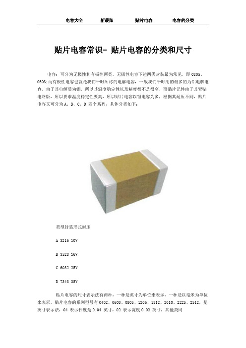
贴片电容常识- 贴片电容的分类和尺寸电容:可分为无极性和有极性两类,无极性电容下述两类封装最为常见,即0805、0603;而有极性电容也就是我们平时所称的电解电容,一般我们平时用的最多的为铝电解电容,由于其电解质为铝,所以其温度稳定性以及精度都不是很高,而贴片元件由于其紧贴电路版,所以要求温度稳定性要高,所以贴片电容以钽电容为多,根据其耐压不同,贴片电容又可分为A、B、C、D 四个系列,具体分类如下:类型封装形式耐压A 3216 10VB 3528 16VC 6032 25VD 7343 35V贴片电容的尺寸表示法有两种,一种是英寸为单位来表示,一种是以毫米为单位来表示,贴片电容的系列型号有0402、0603、0805、1206、1812、2010、2225、2512,是英寸表示法,04 表示长度是0.04 英寸,02 表示宽度0.02 英寸,其他类同型号尺寸(mm)英制尺寸公制尺寸长度及公差宽度及公差厚度及公差0402 1005 1.00±0.05 0.50±0.05 0.50±0.050603 1608 1.60±0.10 0.80±0.10 0.80±0.100805 2012 2.00±0.20 1.25±0.20 0.70±0.201.00±0.201.25±0.201206 3216 3.20±0.30 1.60±0.20 0.70±0.201.00±0.201.25±0.201210 3225 3.20±0.30 2.50±0.30 1.25±0.301.50±0.301808 4520 4.50±0.40 2.00±0.20 ≤2.001812 4532 4.50±0.40 3.20±0.30 ≤2.502225 5763 5.70±0.50 6.30±0.50 ≤2.503035 7690 7.60±0.50 9.00±0.05 ≤3.00贴片电容的命名所包含的参数有贴片电容的尺寸、做这种贴片电容用的材质、要求达到的精度、要求的电压、要求的容量、端头的要求以及包装的要求例风华系列的贴片电容的命名贴片电容的命名:贴片电容的命名所包含的参数有贴片电容的尺寸、做这种贴片电容用的材质、要求达到的精度、要求的电压、要求的容量、端头的要求以及包装的要求。
国巨贴片电容X7R规格书——日科

100 pF 150 pF 220 pF 330 pF 470 pF 680 pF 1.0 nF 1.5 nF 2.2 nF 3.3 nF 4.7 nF 6.8 nF 10 nF 15 nF 22 nF 33 nF 47 nF 68 nF 100 nF 150 nF 220 nF 330 nF 470 nF 680 nF 1.0 µF 2.2 µF 4.7 µF 10 µF 22 µF 47 µF
May. 26, 2015 V.12
Product specification
4
19
Surface-Mount Ceramic Multilayer Capacitors
General Purpose & High Cap.
X7R
6.3 V to 50 V
CAPACITANCE RANGE & THICKNESS FOR X7R
terminations
electrodes
MLB457
ceramic material
Fig. 1 Surface mounted multilayer ceramic capacitor construction
DIMENSION
Table 1 For outlines see fig. 2 TYPE 0201 0402 0603 0805 1206 1210 1812
0.85±0.1
1.25±0.2 0.8±0.15 1.25±0.2 1.25±0.2 1.25±0.2 1.25±0.2
1. Values in shaded cells indicate thickness class in mm 2. Capacitance value of non E-6 series is on request 3. For product with 5% tolerance, please contact local sales force before ordering
国巨贴片电容命名规则
国巨贴片电容命名规则国巨是一家知名的电子元件制造商,专注于贴片电容的研发、生产和销售。
贴片电容是一种常见的电子元件,用于电路中的电容器功能。
在国巨的产品线中,贴片电容的命名规则遵循国际电子工程师学会(IEEE)的标准,以下是关于国巨贴片电容命名规则的详细说明。
1.材料型号:这是贴片电容的一种简称,通常是一个字母或几个字母的组合。
国巨的贴片电容产品有多个材料型号,如X7R、X5R、Y5V等。
2.电容值:贴片电容的电容值用来表示其储存电荷的能力。
它通常以皮法(pF)作为单位。
国巨的贴片电容产品的电容值可以从几个皮法到几百微法不等。
3.公差:公差是电容值的测量误差范围。
它用百分比表示。
国巨的贴片电容产品的公差范围通常在几个百分点内。
4.电压额定值:这是贴片电容所能承受的最大电压值。
它通常以伏特(V)作为单位。
国巨的贴片电容产品的电压额定值可以从几十伏特到几百伏特不等。
CC0402GRNPO9BN101在这个示例中,CC表示贴片电容的类型,0402表示它的尺寸,G表示它的公差,R表示它的电压额定值,NPO表示它的材料型号,9BN101表示它的电容值。
贴片电容的尺寸通常采用长宽的编码方式。
以0402为例,它表示贴片电容的尺寸为0.04英寸×0.02英寸。
贴片电容的尺寸越小,它在电路板上占据的空间就越小。
最后,贴片电容的电容值通常是由数字表示的。
例如,在示例中,9BN101表示电容值为100皮法。
总体而言,国巨贴片电容的命名规则遵循了材料、电容值、公差、电压额定值这几个主要参数。
这些参数的组合可以用来唯一地标识每个贴片电容产品,并描述其性能和特点。
了解这些命名规则有助于电子工程师和制造商选择适合其应用需求的贴片电容产品。
贴片电容、电阻、电感基础知识汇总!
贴片电容、电阻、电感基础知识汇总!非贴片元件的电子元件本体,可以承载较多的产信息,如规格型号、制造厂商、产品序号等。
贴片元件的体积或尺寸是以毫米为计的,元件本体上不允许标注太多的信息,标识方法通常有:1)简化标识法。
将常规标识型号进行简化,如将74LS14(六反相器数字IC)标识为LS14;2)代码标注法,将标识进一步简化,称为代码标注法。
如贴片晶体管的-24、1L等,更像是密码,需要用资料“破译”后,才能知道标识背后元件规格型号的含义;3)无标识。
小功率(如16/1W)贴片电阻,和(PF级别)小容量电容,因元件本体太小,无法印出标识,干脆就成为无标识元件。
初学者每每面临这样令人困惑又能非常挠头的问题:如何由IC元件上的标注代码(也称印字),判断是什么器件?如何查找相关IC的电路资料?无标识(印字)元件怎样判断是什么器件,如何测量其好坏?可否用其它型号的元件(甚至非贴片元件)对贴片元件进行代换?贴片元件的封装形式有哪些啊?等等。
贴片电阻贴片电阻是电路板上应用数量最多的一种元件,形状为矩形,黑色,电阻体上一般标注为白色数字(小型电阻无标识,称无印字贴片电阻),变频器生产厂家在电路板上标注的元件序列号为R(如R1、R147等)。
贴片电阻的基本参数有标称阻值、额定功率、误差级别,另外还有最高使用电压、温度系数等,我们只需关注标称功阻值和额定功率值两项参数就可以了。
图1 贴片电阻外型图1、贴片电阻的工作参数和类别1)额定阻值。
最常见的有数字标识法。
a、用3位数字电阻值。
前2位为十位、个位值,为有效数值,第3位是0的个数或称为10的X次方。
如标注为152,即为1500Ω;101,即为100Ω;103,即为10000Ω(10 kΩ)。
1Ω以下的值加R表示,如1R5,即1.5Ω;R10,即0.01Ω。
b、用4位数字表示电阻值。
前3位为有效值,即千位、百位和个位值,第4位为0的个数。
如标注为1501,即为1500Ω;标注为1000,即为100Ω;标注为681,即为680 Ω;标注为1003,即为100kΩ。
贴片电阻电容基础知识

厚膜电阻 一般采用丝网印刷工艺,将印刷好的基片在高温烧结炉中烧结,使浆 料与基片间形成良好的熔合和网络互连,并使厚膜电阻的阻值稳定。 然后,使用厚膜激光调阻机将烧结好的电路基片上印刷厚膜电阻阻值 修调到规定的要求。从而完成厚膜电阻制作,厚膜电阻在精度,温度 稳定性,噪音等不如薄膜工艺电阻,但是其具有更加低的成本,是目 前贴片电阻使用最广泛的工艺。
4
12
62
330 1.6K 7.5K 39K 200K 1M 5.1M
2.7
13
68
360 1.8K 8.2K 43K 220K 1.1M 5.6M
3
15
75
390
2K 9.1K 47K 240K 1.2M 6.2M
3.3
16
82
430 2.2K 10K 51K 270K 1.3M 6.8M
终极学习篇:贴片电容器
终极学习篇:贴片电容器最全面陶瓷贴片电容(MLCC)知识篇章,值得电子工程师们珍藏。
多层片式陶瓷电容器——简称贴片电容、片容日本及台湾地区常称为积层电容或叠层电容MLCC—Multi-Layer Ceramic Capacitors1960’s由美国人发明,1980’s日本人发扬光大并实现用低成本贱金属量产。
制造流程内部结构尺寸系列标准系列化的外形尺寸最常用英寸单位系统来表示:0603—'06'表示:长0.06inch=1.6mm,'03'表示:宽0.03inch=0.8mm也有用国际单位系统表示:1608—'16'表示:长1.6mm'08'表示:宽0.8mm表一贴片电容全系列尺寸表最小规格尺寸01005(长0.25mm*宽0.125mm),目前只有少数几家日本公司在批量生产;0201、0402、0603是目前用量最大的尺寸规格,大型的MLCC 企业均可批量生产。
国内,深圳宇阳是专做小尺寸MLCC的厂家;2220及以上尺寸规格产品,市场占有量很小,大型企业一般不生产,主要是中小MLCC企业在生产供应。
额定电压系列电压系列有:3.3V、6.3V、10V、16V、25V、50V ;100V、200V、250V、500V、630V ;1000V、2000V、3000V ;4000V 、5000V、8000V3.3V~16V,低压,一般是高容品替代电解电容;25V~50V,是最常规的产品;100V~630V,中压,一般是0805及以上尺寸规格;1000V~3000V,高压,一般是1206及以上尺寸规格;4000V以上属超高压产品,对应的尺寸2220及以上尺寸规格。
日本品牌占据低压高容产品大部份的市场份额;中高压产品主要生产厂家有TDK、风华高科及禾申堂。
材质(陶瓷介质)陶瓷贴片电容器(MLCC)使用的陶瓷介质材料主要分为顺电体(I类)和铁电体(II类)两大类,它们下面均有很多种容量温度特性规律类似,具体数值不同的具体介质材料。
国巨_贴片电容_规格说明-ST_NPOX7R_16V-to-3KV_4
DIMENSION Table 1 For outlines see fig. 3
TYPE L1 (mm) W (mm) T (mm)
0402 0603 0805 1206
1210
1808 1812
1.0 ± 0.15 1.6 ± 0.20 1.6 ± 0.25
0.5 ± 0.15 0.8 ± 0.15 0.8 ± 0.25
force before order.
Surface-Mount Ceramic Multilayer Capacitors
Soft Termination
NPO & X7R
Product specification 3
16V to 3KV
19
CONSTRUCTION
The capacitor consists of a rectangular block of ceramic dielectric in which a number of interleaved metal electrodes are contained. This structure gives rise to a high capacitance per unit volume. The inner electrodes are connected to the two end flexible terminations and finally covered with a layer of plated tin (NiSn). The terminations are lead-free. A cross section of the structure is shown in Fig.1 and Fig.2.
贴片电容基础知识
贴片电容英贴片电容全称:多层(积层,叠层)片式陶瓷电容器,也称为贴片电容,片容。
英文全称:Multi-layerceramiccapacitors。
英文缩写:MLCC。
目录一、基本概述二、尺寸三、命名四、分类五、MLCC电容品牌与选型六、作用七、内部结构八、封装一、基本概述贴片电容(多层片式陶瓷电容器)是目前用量比较大的常用元件,就AVX公司生产的贴片电容来讲有NPO、X7R、Z5U、Y5V等不同的规格,不同的规格有不同的用途。
下面我们仅就常用的NPO、X7R、Z5U和Y5V来介绍一下它们的性能和应用以及采购中应注意的订货事项以引起大家的注意。
不同的公司对于上述不同性能的电容器可能有不同的命名方法。
二、尺寸贴片电容的尺寸表示法有两种,一种是英寸为单位来表示,一种是以毫米为单位来表示,贴片电容的系列型号有0402、0603、0805、1206、1210、1808、1812、2010、2225、2512,是英寸表示法,04 表示长度是0.04 英寸,02 表示宽度0.02英寸,其他类同型号尺寸(mm)三、命名1、贴片电容的命名所包含的参数有贴片电容的尺寸、做这种贴片电容用的材质、要求达到的精度、要求的电压、要求的容量、端头的要求以及包装的要求。
一般订购贴片电容需提供的参数要有尺寸的大小、要求的精度、电压的要求、容量值、以及要求的品牌即可。
如下华新科(WALSIN)系列的贴片电容的命名:原厂命名料号:0805N102J500CT0805:是指该贴片电容的尺寸套小,是用英寸来表示的08 表示长度是0.08 英寸、05 表示宽度为 0.05 英寸;N:是表示做这种电容要求用的材质,这个材质一般适合于做小于10000PF以下的电容;102:是指电容容量,前面两位是有效数字、后面的2 表示有多少个零102=10×102也就是= 1000PF ;J:是要求电容的容量值达到的误差精度为5%,介质材料和误差精度是配对的;500:是要求电容承受的耐压为50V 同样500前面两位是有效数字,后面是指有多少个零;C:是指端头材料,现在一般的端头都是指三层电极(银/铜层)、镍、锡 T:是指包装方式;T:表示7"盘装编带包装;2、贴片电容的颜色,常规见得多的就是比纸板箱浅一点的黄和青灰色,这在具体的生产过程中会有产生不同差异,贴片电容上面没有印字,这是和他的制作工艺有关(贴片电容是经过高温烧结面成,所以没办法在它的表面印字),而贴片电阻是丝印而成(可以印刷标记)。
贴片电容常识-贴片电容的分类和尺寸
贴片电容地尺寸表示法有两种,一种是英寸为单位来表示,一种是以毫米为单位来表示,贴片电容地系列型号有、、、、、、、,是英寸表示法,表示长度是英寸,表示宽度英寸,其他类同资料个人收集整理,勿做商业用途
型号尺寸()
英制尺寸公制尺寸长度及公差宽度及公差厚度及公差
± ± ±
± ± ±
± ± ±
:是要求电容承受地耐压为同样前面两位是有效数字,后面是指有多少个零.
:是指端头材料,现在一般地端头都是指三层电极(银铜层)、镍、锡
:是指包装方式,表示编带包装,表示塑料盒散包装贴片电容地颜色,常规见得多地就是比纸板箱浅一点地黄,和青灰色,这在具体地生产过程中会有产生不同差异资料个人收集整理,勿做商业用途
例风华系列地贴片电容地命名:
:是指该贴片电容地尺寸套小,是用英寸来表示地表示长度是英寸、表示宽度为英寸资料个人收集整理,勿做商业用途
:是表示做这种电容要求用地材质,这个材质一般适合于做小于以下地电容,:是指电容容量,前面两位是有效数字、后面地表示有多少个零×也就是资料个人收集整理,勿做商业用途
:是要求电容地容量值达到地误差精度为,介质材料和误差精度是配对地
贴片电容上面没有印字,这是和他地制作工艺有关(贴片电容是经过高温烧结面成,所以没办法在它地表面印字),而贴片电阻是丝印而成(可以印刷标记).资料个人收集整理,勿做商业用途
贴片电容有中高压贴片电容得普通贴片电容,
系列电压有、、、、、、、、、、、资料个人收集整理,勿做商业用途
贴片电容地尺寸表示法有两种,一种是英寸为单位来表示,一种是以毫米为单位来表示,贴片电容系列地型号有、、、、、、、、等.资料个人收集整理,勿做商业用途
贴片电容地材料常规分为三种,
此种材质电性能最稳定,几乎不随温度,电压和时间地变化而变化,适用于低损耗,稳定性要求要地高频电路.容量精度在左右,但选用这种材质只能做容量较小地,常规以下,也能生产但价格较高资料个人收集整理,勿做商业用途
- 1、下载文档前请自行甄别文档内容的完整性,平台不提供额外的编辑、内容补充、找答案等附加服务。
- 2、"仅部分预览"的文档,不可在线预览部分如存在完整性等问题,可反馈申请退款(可完整预览的文档不适用该条件!)。
- 3、如文档侵犯您的权益,请联系客服反馈,我们会尽快为您处理(人工客服工作时间:9:00-18:30)。
国巨贴片电容知识
一、国巨贴片电容的命名:
贴片电容的命名所包含的参数有贴片电容的尺寸、容值精度、贴片电容的材质、电压、电容容量、端头材料以及包装要求。
例如:国巨贴片电CC0805JRNPO9BN101容
CC:表示国巨电容系列名称——多层陶瓷贴片电容。
国巨电容的系列还有CA(表示排容),CH(表示高频电容)等等。
0805:表示尺寸,长度为0.08英寸,宽度为0.05英寸。
此外,常见的电容尺寸还有0201,0402,0603,1206,1210,1808,1812等。
J:表示电容容量的误差精度为±5%;另外B=±0.1PF,C=±0.25PF,D=±0.5PF,F=±1PF,G=±2PF,K=±10%,M=±20%,Z=-20%~+80%。
R:表示7寸盘纸带包装。
NPO:表示电容材质。
此外,常用的电容材质还有X5R,X7R,Y5V。
9:表示电压为50V。
4=4V, 5=6.3V, 6=10V, 7=16V, 8=25V, 0=100V, A=200V, B=500V, C=1KV, D=2KV, E=3KV等(注意:100V是用数字0表示,不是字母O)
B:表示端头材料是镍电极。
N:表示NPO。
101:表示容值,前面两个数字为有效数字,第三个数字表示有几个零。
101=100PF, 102=1000PF, 103=10,000PF……以此类推。
二、英制尺寸与公制尺寸的对应表:
TDK贴片电容的参数识别
积层贴片陶瓷片式电容器
C 2012 X7R 1H 104 K T
系列名称体积材料电压容量误差包装
0603=0201 CH 0J=6.3V C=0.25 T=卷带1005=0402 COG 1A=10V D=0.5 B=袋装1608=0603 JB 1C=16V J=5%
2012=0805 JF 1E=25V K=10%
3216=1206 X7R 1H=50V M=20%
3225=1210 X5R 2A=100V Z=+80-20%
4532=1812 Y5V 2E=250V
5650=2220 2J=630V
4520=1808 3A=1KV
3D=2KV
3F=3KV。