CC2500控制输出功率
邦定CC2500模块2.4G
w w w. h k w r f . c o m
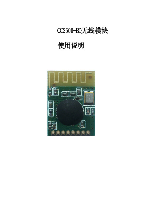
CC2500-BD 无线模块
接口说明
引脚定义
引脚 GND 3.3V SI SCLK SO GDO2 GDO0 CSN 类型 电源地 工作电源 SPI数据 SPI时钟 SPI数据 数字I/O 数字I/O SPI片选 描述 和系统共地 电源电压,直流1.8~3.6V输入 SPI数据输入 SPI时钟输入 SPI数据输出 可配置以产生触发信号或时钟信号 可配置以产生触发信号或时钟信号 CSN=0有效
CC2500-BD 无线模块
使用说明
CC2500-BD 无线模块
概述
CC2500BD基于 TI Chipcon 的 CC2500 无线收发芯片设计,是一款完整的、体积小巧的、低功耗
的无线收发模块。 CC2500 是 TI Chipcon 推出的 2.4GHz 频段无线收发芯片之一, 最大输出功率可为+1dBm, 最高传输速率达 500Kbps。模块集成了所有射频相关功能和器件,并有 PCB 天线,不需再配置天线即可获 得很的射频性能。用户不需要对射频电路设计深入了解,就可以使用本模块轻易地开发出性能稳定、可靠 性高的无线产品。
w w w. h k w r f . c o m www. h k w r f . c o m
CC2500-BD 无线模块
工作模式
CC2500 的工作模式主要有休眠模式、空闲模式、发射模式和接收模式,休眠模式下功耗可降到最低。 从休眠模式下唤醒后, 进入空闲模式。 除休眠模式外, 各模式之间可相互切换, 也可配置为自动切换。 CC2500 的主要工作状态图如下图所示,详细描述请参考 CC2500 芯片规格书。
w w w. h k w r f . c o m www. h k w -BD 无线模块
CC2500寄存器设置
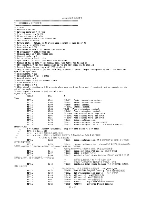
//========================================================// CC2500寄存器中的数据//========================================================// 2.4GHz// Product = CC2500// Crystal accuracy = 40 ppm// X-tal frequency = 26 MHz// RF output power = 0 dBm// RX filterbandwidth = 232.000000 kHz// Deviation = 0.000000// Return state: Return to RX state upon leaving either TX or RX// Datarate = 10.000000 kbps// Modulation = 2-FSK// Manchester enable = (0) Manchester disabled// RF Frequency = 2433.000000 MHz// Channel spacing = 199.950000 kHz// Channel number = 0// Optimization = Sensitivity// Sync mode = (3) 30/32 sync word bits detected// Format of RX/TX data = (0) Normal mode, use FIFOs for RX and TX// CRC operation = (1) CRC calculation in TX and CRC check in RX enabled// Forward Error Correction = (0) FEC disabled// Length configuration = (1) Variable length packets, packet length configured by the first received byte after sync word.// Packetlength = 255// Preamble count = (2) 4 bytes// Append status = 1// Address check = (0) No address check// FIFO autoflush = 0// Device address = 0// GDO0 signal selection = ( 6) Asserts when sync word has been sent / received, and de-asserts at the end of the packet// GDO2 signal selection = (11) Serial ClockRF_REGISTER_TAB:ADDAR PCL, R//===RETIA 0X04 ;//0x07 Packet automation control.RETIA 0X05 ;//0x08 Packet automation controlRETIA 0X00 ;//0x09 Device address.RETIA 0X00 ;// 0X0A Channel number.RETIA 0X0B ;//0x0B Freq synthesizer control.RETIA 0X00 ;//0x0C Freq synthesizer control.RETIA 0x5D ;// 0X0D Freq control word, high byteRETIA 0x93 ;// 0X0E Freq control word, mid byte.RETIA 0xB1 ;// 0X0F Freq control word, low byte.RETIA 0x78 ;//0x10 Modem configuration.RETIA 0x93 ;//0x11 Modem configuration (DATARATE)RETIA 0x83 ;//0x12 Modem configuration. BIT7:0 = Enable (better sensitivity)// 1 = Disable (current optimized). Only for data rates ≤ 250 kBaud// BIT6:4 = 0x111 MSK// BIT3 = 0 禁止曼切斯特编码/译码// BIT2:0 = 0X011 开启TX时的重复同步词汇发送和RX时的32 位同步词汇侦测// (只有32 位中的30 位需要匹配):RETIA 0x22 ;//0x13 Modem configuration. 禁止前导位纠错;前导4个字节;信道空间的2个指数RETIA 0xF8 ;//0x14 Modem configuration. (channal)信道空间(初始为1)的8位尾数26000000/2^18*(256+0xF8)*2^2*(channal)=199.951171875khz// 此信道的频率单位与基频相加后,就是运行的频率RETIA 0x44 ;//0x15 Modem dev (when FSK mod en) 背离指数为0RETIA 0x07 ;//0x16 MCSM2 至到数据包终止RETIA 0x30 ;//0x17 MainRadio Cntrl State Machine 若RSSI 在门限之下,清理数据包指示,除非当前接收一个数据包// 在数据包被接受后的下一个状态:空闲// 在数据包已发送到(TX)后的下个状态:空闲RETIA 0x18 ;//0x18 MainRadio Cntrl State Machine 当从空闲到TX 或RX时,进行自动校准// 终止次数64次,禁止引脚通讯控制选项,XOSC_FORCE_OFFRETIA 0x16 ;//0x19 Freq Offset Compens. Config 频率偏移补偿配置RETIA 0x6C ;//0x1A Bit synchronization config. 位同步控制RETIA 0x43 ;//0x1B AGC control. AGC控制寄存器RETIA 0x40 ;//0x1C AGC control AGC控制寄存器RETIA 0x91 ;//0x1D AGC control AGC控制寄存器RETIA 0x87 ;//0X1E WOREVT1 High Byte Event0 TimeoutRETIA 0x6B ;//0X1F WOREVT0 Low Byte Event0 TimeoutRETIA 0xF8 ;//0X20 WORCTRL Wake On Radio ControlRETIA 0x56 ;//0X21 Front end RX configuration. 前端rx配置RETIA 0x10 ;//0X22 Front end RX configuration 前端TX配置,调整当前TX LO 缓冲(输入到PA)RETIA 0xA9 ;//0x23 Frequency synthesizer cal 频率合成器校准配置和结果寄存器RETIA 0x0A ;//0x24 Frequency synthesizer cal. FSCAL3CHIP_CURR_CAL_EN FSCAL3RETIA 0x00 ;//0X25 Frequency synthesizer calibration.RETIA 0x11 ;//0X26 Frequency synthesizer calibration.(38);=========================================================; 初始化德州仪器CC2500//========================================================INSTALL_CC2500:/*让CC2500进入待机模式*/MOVIA CC2500_SIDLE ;让CC2500先工作起来,命令滤波CALL HAND_SPI_WRITE//====重启CC2500芯片 时序上的延时BSR CSN ;关闭芯片的选择CALL DELAY100US ;状态延时BCR CSN ;开启芯片的选择CALL DELAY100US ;状态延时BSR CSNCALL DELAY100US ;延时200微秒CALL DELAY100USBCR CSN ;选择CC2500BTRSC SO //等待CC2500的电压调制器稳定GOTO $-1MOVIA CC2500_SRES //重启CC2500芯片CALL HAND_SPI_WRITEBSR CSNBCR SCLK //关闭CC2500的选择BCR SI/*设置CC2500的寄存器*/MOVIA 0X20 ;数据个数32MOVAR COUNTER1MOVIA 0X07MOVAR TEMP1 ;地址的初始值REGISTER_LOOP:BCR CSN ;选择CC2500芯片BTRSC SO ;等待SO腿输出低电平GOTO $-1BCR SCLK ;数据的时钟线变低,锁住数据线上的电平MOVR TEMP1, AANDIA 0X7F ;写第一个数据,第7位必须为低电平表示写(时序图上是这样描述的)MOVAR WRITE_VALUE ;写寄存器的初始值CALL SPI_WRITEMOVR TEMP1, AADDIA 0XF9 ;相当A-07HCALL RF_REGISTER_TAB ;查表指令MOVAR WRITE_VALUE ;写进寄存器的的数据CALL SPI_WRITEINCR TEMP1, R ;寄存器的地址加一BCR SIBSR CSN ;由于每次都是突发访问,根据芯片的说明,突发位的访问不管是读还是写,读必须通过设置CSN为高来终止芯片的选择DECRSZ COUNTER1, RGOTO REGISTER_LOOP ;循环写入32个数据/*设置CC2500的IOCFG2*/MOVIA 0X00 //寄存器0MOVAR TEMP1MOVIA 0X29 //数据0BMOVAR TEMP2CALL DOUBLE_DATANOPNOP //空指令/*设置CC2500的IOCFG0 非温度检测,不反转,当同步词汇被送出/收到时声明,在数据包末端时反声明。
基于CC2500的低成本和低功率的无线收发器电路设计
通信原理课程设计题目:基于CC2500的低成本和低功率的无线收发器电路设计专业班级:电子信息工程021班*名:**学号:***********指导老师:***设计时间:2005年5月24日到6月3日目录1 CC2500芯片介绍 (3)2 芯片主要性能指标 (4)2.1 参数额定值 (5)2.2 工作环境 (5)2.3 工作电流的说明 (5)2.4 一般特性 (6)2.5 射频接收部分 (6)2.6 射频发射部分 (7)2.7 晶体振荡器 (7)2.8 低功率RC振荡器 (8)2.9 频率合成器特性 (8)2.10 模拟温度传感器 (9)2.11 直流特性 (10)2.12 电源启动复位 (10)3 芯片封装与引脚功能 (10)4 内部结构与工作原理 (12)4.1 CC2500内部模块结构 (12)4.2 微控制器接口和引脚结构 (13)4.3 数据传输速率的设计 (14)4.4 接收机信道滤波带宽的控制 (14)4.5 解调器、符号同步装置和数据的设定 (15)4.6 数据处理的硬件支持 (16)4.7 调制方式 (19)4.8 接收信号的限定和链接质量消息 (19)4.9 频率设计 (21)4.10 VCO的特点 (21)4.11 电压调整器 (21)4.12 天线接口(Interface) (22)4.13 常规用途/输出控制引脚测试 (22)4.14 异步的和同步的串联操作 (22)4.15 外部工作状态 (23)5 应用电路的设计 (23)5.1 偏压电阻器 (25)5.2 Balun(不平衡变压器和射频匹配) (25)5.3 晶体 (26)5.4 电源去耦 (26)5.5 设计总电路 (29)6 设计总结 (30)7 参考文献 (27)附录1 (27)附录2 (29)基于CC2500的低成本和低功率的无线收发器电路设计指导教师:黄智伟陈雄陈细芳谭小强胡亮摘要:CC2500是专用来设计低成本低功率频率可达到2.4GHz的无线电收发器芯片。
2.4G无线数传模块电路
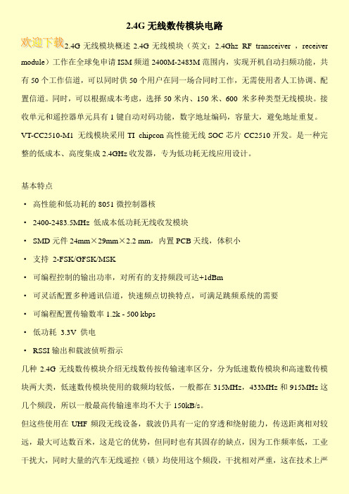
2.4G无线数传模块电路2.4G无线模块概述2.4G无线模块(英文:2.4Ghz RF transceiver ,receiver module)工作在全球免申请ISM频道2400M-2483M范围内,实现开机自动扫频功能,共有50个工作信道,可以同时供50个用户在同一场合同时工作,无需使用者人工协调、配置信道。
同时,可以根据成本考虑,选择50米内、150米、600 米多种类型无线模块。
接收单元和遥控器单元具有1键自动对码功能,数字地址编码,容量大,避免地址重复。
VT-CC2510-M1 无线模块采用TI chipcon高性能无线SOC芯片CC2510开发。
是一种完整的低成本、高度集成2.4GHz收发器,专为低功耗无线应用设计。
基本特点·高性能和低功耗的8051微控制器核·2400-2483.5MHz 低成本低功耗无线收发模块·SMD元件24mm×29mm×2.2 mm,内置PCB天线,体积小·支持2-FSK/GFSK/MSK·可编程控制的输出功率,对所有的支持频段可达+1dBm·可灵活配置多种通讯信道,快速频点切换特点,可满足跳频系统的需要·可编程配置传输数率1.2k - 500 kbps·低功耗3.3V 供电·RSSI输出和载波侦听指示几种2.4G无线数传模块介绍无线数传按传输速率区分,分为低速数传模块和高速数传模块两大类,低速数传模块使用的载频均较低,一般都在315MHz,433MHz和915MHz这几个频段,所以一般最高传输速率均不大于150kB/s。
但这些使用在UHF频段无线设备,载波仍具有一定的穿透和绕射能力,传送距离相对较远,最大可达数百米,这是它的优势,但同时也有其固存的缺点,因为工作频率低,工业干扰大,同时大量的汽车无线遥控(锁)均使用这个频段,干扰相对严重,这在技术上严。
500T履带吊的性能介绍(阅读)

4.起重性能表的查阅及工况的使用
1)在起吊重物的安全作业范围内,增大作业半 径,但有时受场地的限制,不能达到超起配重 离地的目的。 2)将重物放到地面上,用辅助吊车去掉一部分 超起配重。 3)将重物放到地面上,将超起配重的半径调整 到小级别的位置。
5.履带吊的安全使用
(一)一般规定:
1. a sufficient safety clearance must be maintained between the crane (and hoist rope, lifting tackle, hook block, load) and current−carrying lines. 在吊车(包括起升绳、吊具、吊钩、吊重) 与输电线之间要有足够的安全距离。
3.起重性能表中的标注
C标注说明
Danger of tipping backwards of jib! 谨防防副臂向后倾翻的危险! Capacities only valid without set of sheaves on main boom. 此表中的额定起重量仅在主臂顶部未安装滑 轮组时有效!
3.起重性能表中的标注
C标注说明
6) Loads in brackets () do not lift off SL-counterweight. 带括号的额定负荷表示超起配重可能不离 地 In case of runner mounted: reduce the load! 在安装鹰嘴的情况下要减负荷使用!
4.起重性能表的查阅及工况的使用
3 . 在场地狭小的地点,必须考虑主臂、 副臂会不会各构建物发生干涉,主臂角 度最大能到87 °,副臂角度在起重性能表中
没有,可根据幅度和履带吊各机构之间的位置 数据求得。还应考虑主机尾部空间是否足够大, 能否使用超起装置。
基于CC2500的2.4G无线收发系统设计正文 免费下载

基于CC2500的2.4GHz无线收发系统设计1.系统方案设计与论证1.1设计要求利用无线芯片设计一个无线收发系统,要求设计达到以下技术要求:①低工作电压,低功耗。
②工作于免费的2.4~2.485GHz免许可证ISM频段。
③各主要技术指标可实现编程控制,要求操作简单。
④高信息传输速率(≥250kbps),支持多种调制方式。
⑤高接收灵敏度(10kbps下-100dBm;250kbps下-90dBm;1%数据包误码率,450KHz数字信道滤波带宽),可编程输出功率控制。
⑥可实现点对多点通信地址控制。
1.2设计方案与论证设计采用模块化设计,整个系统主要由无线收发模块、控制模块和电源模块构成。
1.2.1无线模块根据设计要求,查找工作在2.4GHz频段相应无线收发芯片的datasheeet,从Nordic、Maxic、TI、Silicon Labs等各大公司生产的无线收发芯片中仔细查找筛选,筛选的原则是:①满足设计性能要求②价格合理,容易购买③设计难度小,操作方便。
通过比较,最终选定TI公司的CC2500作为无线模块核心。
CC2500体积小,几乎集成了所有的无线射频功能,灵敏度高,可编程设定主要工作参数,高效的SPI接口,工作在1.8V~3.6V电压范围,功耗低,具有多种调制方式,能满足不同应用要求,纠错能力强、误码率低。
所需外围器件很少,降低了设计难度;数字特征明显,软件设计难度降低,用户操作也更加简单;收发一体,可实现双向通信。
所以,选择CC2500作为无线核心具有很大的设计优势和价格优势,设计周期短,使用简便,最终产品也能够更快的占领市场。
1.2.2控制模块无线模块选用了CC2500,由于CC2500芯片内部集成了几乎所有的射频功能,控制器只要能控制 C C2500的不同操作模式,写入缓冲数据,通过4线SPI(SI,SO,SCLK 和 C Sn)总 线配置接 口读回状态信息就能达到要求。
因此,廉价的MCU就能对其进行控制,市场上最常见的8位51系列单片机就能满足要求,综合性能、价格、应用普遍性等多方面的因素,本设计采用能满足设计要求、性能适中、价格最便宜、使用广泛的STC89C52单片机作为无线模块微控制核心。
CC2500经验
单片机 程序下载
/search.php?key=CC2500&format=
可以把GDO2引脚配置成每发射或接收一个包申明(GDO2_CFG写0x06),
这样,若发射或接收了数据,就会在GDO2引脚出现方波。
例如,在接收过程中,用示波器测试GDO2引脚出现了方波,
但是程序里没有接收到数据。此时可以认为CC2500接收到了数据包,此时可以从晶振时钟及数据包格式考虑可能出现的问题
4. CC2500引脚配置不正确。在用MCU控制CC2500芯片的工作时,用来连接GDO0、GDO2、MISO的MCU引脚应该配置为漏极开路。若配置成推挽输出,
则电路无法进行收发。
CSN, MOSI, SCK最好配置成推挽输出。
在调试中,可以结合程序,对CC2500出现的问题进行判断
。例如引脚的调试经验。若CC2500不能正常工作,常见的原因有以下几种:
1. CC2500芯片引脚虚焊。CC2500是QFN封装的,引脚在芯片背面,在手工吹焊时常容易出现虚焊,而不能正常工作。
2. CC2500天线接口的电感,电容取值不正确。CC2500的天线接口由∏型阻抗匹配网络和平衡滤波网络组成。
在实际使用中,虽然电感、电容取值是按照Datasheet的参考值选取的,
但是经常会出现电感、电容的真实值和标定值相差过大,
从而导致CC2500电路无法正常发射和接收。我就有一次,买了1.5pF的电容,
结果对方给了我220pF的电容。所以,在焊接电感电容前需要核对。
3. 26MHz晶振。 遇到过晶振不振,CC2500无法工作的情况。还遇到过进行通讯的两块CC2500电路板使用了不同品牌的晶振,结果时钟不一致,导致无法进行收发。
SmartRF Studio 使用教程 - 参数配置部分介绍
SmartRF Studio 使用教程(1)在SmartRF Studio程序中对CC1101进行参数配置和生成配置文件文档编号:NOVATE_NOTE_20150730版权所有:NOVATE 2015 ALL RIGHT RESERVEDMENU / 目录下载与安装 (2)启动界面 (3)SmartRF Studio 7 (3)SmartRF Studio 6 (4)配置界面 (5)SmartRF Studio 7 (5)快速配置区 (6)射频参数设置区 (7)寄存器查看器 (8)在线仿真区 (8)SmartRF Studio 6 (9)射频参数设置区 (10)在线监视区和收发调试区 (12)简介SmartRF Studio是由TI公司提供的一款专用于CC系列射频芯片的通用配置与在线编程的应用程序。
在使用与调试CC系列芯片时,通常需要使用该软件完成相应寄存器的配置工作,同时该软件也提供对一些芯片的在线仿真功能。
SmartRF Studio支持TI所有型号的射频芯片。
目前最新版本为SmartRF Studio 7,但是使用一些较早期芯片型号(如CC1100)时建议使用SmartRF Studio的早期版本。
下载与安装首先可以去TI官方网站获取SmartRF Studio软件的安装包文件,截至2015年7月份的最新版本为7.2.1.0。
同时网站还提供早期版本的SmartRF Studio软件安装包提供下载。
当您使用CC1100或CC1101芯片时,建议选用6.13.1版本的SmartRF Studio软件。
软件下载页面:/tool/cn/SMARTRFTM-STUDIO安装包文件下载后可直接进行安装,通常选择默认参数进行安装即可。
在下面的介绍中会分别对SmartRF Studio 7 和SmartRF Studio 6 两种版本的程序进行说明。
启动界面SmartRF Studio 7安装结束后使用运行SmartRF Studio程序即会出现上图所示的界面,在该界面中可以选择需要的CC系列射频芯片的型号。
CC2500控制输出功率
Programming Output Power on CC2500 and CC2550By Charlotte Seem Keywords•PATABLE Register Settings •Output Power Levels •Current Consumption •CC2500•CC25501 IntroductionThe CC2500 and CC2550 RF output power level is set by the PATABLE register setting. This register setting also influences the power levels at the different harmonics and the current consumption for the device. These parameters must therefore be considered when choosing the optimal register settings. This document gives complete CC2500 and CC2550 PA tables with typical output power, harmonics, and current consumption for the different register settings at 25 °C and 3.0 V supply voltage.Table of Contents KEYWORDS (1)1INTRODUCTION (1)2ABBREVIATIONS (2)3OUTPUT POWER FOR THE DIFFERENT PATABLE REGISTER SETTINGS (3)3.1CC2500 (3)3.2CC2550 (7)4GENERAL INFORMATION (12)4.1D OCUMENT H ISTORY (12)2 AbbreviationsfrequencyRadioRF3 Output Power for the Different PATABLE Register SettingsThe CC2500 and CC2550 RF output power level is decided by values set in the PATABLE register and the FREND0.PA_POWER value. The 8-byte PATABLE register will, as described in the CC2500 and CC2550 datasheets, set the PA power control settings while the 3-bit FREND0.PA_POWER value selects the PATABLE entry to be used.The typical CC2500 output power levels and current consumption for the different PATABLE register settings are given in Table 1. The equivalent parameters for CC2550 are given in Table 2. It is important to notice from these tables that the output power levels for the different register values are not linear. Also note that a decrease in output power level not necessarily means a decrease in the current consumption or in the harmonics power level.3.1 CC2500Power Table for CC2500 Power @2 440 MHz[dBm]Power @2nd harm4 880 MHz[dBm]Power @3rd harm7 320 MHz[dBm]Power @4th harm9 760 MHz[dBm]Power @5th harm12 200MHz [dBm]Current[mA]Register Value: FF 1,5 -45,5 -57,0 -52,5 -57,9 21,4 Register Value: EF 1,1 -43,1 -56,2 -54,0 -58,2 19,8 Register Value: FB 1,1 -45,8 -57,3 -54,3 -57,6 21,0 Register Value: EB 0,7 -43,5 -56,7 -54,2 -57,9 19,4 Register Value: FE 0,3 -54,2 -57,0 -58,4 -58,3 21,1 Register Value: EE 0,0 -49,5 -57,1 -58,7 -58,2 19,5 Register Value: FD -0,1 -55,3 -57,5 -58,8 -57,9 21,1 Register Value: FA -0,2 -53,3 -56,5 -58,7 -58,0 20,7 Register Value: ED -0,4 -52,3 -57,0 -58,5 -58,2 19,5 Register Value: EA -0,4 -50,3 -56,6 -57,5 -57,9 19,1 Register Value: F9 -0,6 -54,5 -56,7 -58,4 -58,3 20,7 Register Value: E9 -0,8 -51,9 -57,1 -57,8 -57,9 19,1 Register Value: BF -1,3 -45,8 -56,9 -56,5 -58,8 18,1 Register Value: BB -1,8 -46,3 -57,0 -57,1 -57,8 17,7 Register Value: AF -1,9 -43,7 -56,9 -57,7 -58,1 17,0 Register Value: AB -2,3 -44,5 -57,0 -56,8 -58,4 16,6 Register Value: BE -2,7 -54,1 -57,1 -58,7 -58,3 17,8 Register Value: BD -3,1 -55,0 -57,7 -58,1 -58,4 17,7 Register Value: AE -3,1 -49,9 -56,8 -58,2 -57,7 16,7 Register Value: BA -3,1 -53,5 -56,6 -58,6 -58,9 17,4 Register Value: AD -3,5 -51,9 -56,1 -57,9 -58,0 16,6 Register Value: B9 -3,5 -54,7 -57,1 -58,4 -58,2 17,3 Register Value: AA -3,5 -50,8 -56,8 -58,8 -58,0 16,3 Register Value: DF -3,7 -38,3 -57,0 -50,7 -57,9 15,1 Register Value: DB -3,8 -38,8 -55,7 -52,4 -57,3 14,8 Register Value: A9 -3,8 -52,7 -57,1 -58,2 -58,6 16,2 Register Value: DE -4,3 -40,7 -56,8 -54,4 -57,8 14,8 Register Value: DA -4,4 -41,3 -57,1 -57,5 -58,0 14,4 Register Value: DD -4,4 -41,4 -56,6 -56,4 -58,3 14,7 Register Value: D9 -4,6 -42,1 -57,4 -56,9 -58,1 14,4 Register Value: F7 -4,7 -45,1 -57,6 -58,8 -57,7 19,9 Register Value: E7 -4,7 -44,6 -57,8 -59,1 -58,5 18,2 Register Value: F6 -5,5 -48,0 -56,5 -58,7 -57,9 19,6 Register Value: E6 -5,5 -47,4 -57,1 -58,6 -58,4 17,9 Register Value: F5 -5,7 -48,6 -56,6 -58,8 -58,5 19,5Power Table for CC2500 Power @2 440 MHz[dBm]Power @2nd harm4 880 MHz[dBm]Power @3rd harm7 320 MHz[dBm]Power @4th harm9 760 MHz[dBm]Power @5th harm12 200MHz [dBm]Current[mA]Register Value: E5 -5,7 -48,0 -56,8 -58,5 -58,1 17,8 Register Value: 7F -6,1 -47,8 -56,9 -58,2 -58,2 15,0 Register Value: 7B -6,5 -48,4 -57,5 -58,6 -57,4 14,6 Register Value: D7 -6,8 -43,7 -56,8 -57,6 -58,4 13,5 Register Value: 6F -6,8 -45,5 -57,1 -58,9 -58,0 14,5 Register Value: 9F -7,0 -40,2 -57,0 -54,7 -58,4 13,9 Register Value: 6B -7,2 -47,3 -57,1 -58,5 -58,1 14,1 Register Value: 9B -7,2 -40,5 -57,3 -55,5 -57,9 13,5 Register Value: D6 -7,4 -46,4 -56,5 -58,4 -57,4 13,1 Register Value: 7E -7,5 -55,1 -56,9 -59,1 -58,2 14,7 Register Value: B7 -7,6 -46,3 -56,9 -58,5 -58,2 16,5 Register Value: D5 -7,6 -47,0 -56,8 -59,3 -58,2 13,1 Register Value: 9E -7,7 -42,6 -57,3 -56,2 -58,3 13,5 Register Value: A7 -7,7 -46,1 -56,1 -58,5 -58,4 15,4 Register Value: 7D -7,8 -56,3 -57,5 -58,2 -57,5 14,6 Register Value: 9A -7,8 -43,1 -57,3 -58,4 -58,3 13,2 Register Value: 9D -7,9 -43,4 -56,9 -57,4 -58,0 13,5 Register Value: 7A -7,9 -55,4 -57,0 -58,8 -58,5 14,3 Register Value: 6E -8,0 -51,9 -56,6 -58,0 -58,4 14,1 Register Value: 99 -8,0 -44,0 -56,8 -58,4 -58,5 13,1 Register Value: 79 -8,3 -56,4 -56,8 -58,4 -57,6 14,3 Register Value: 6D -8,3 -54,8 -56,6 -58,3 -58,2 14,1 Register Value: B6 -8,3 -49,6 -57,4 -58,6 -58,4 16,2 Register Value: 6A -8,4 -53,5 -56,7 -58,6 -58,1 13,7 Register Value: A6 -8,4 -48,7 -56,7 -58,7 -58,2 15,0 Register Value: B5 -8,5 -50,1 -57,1 -58,9 -58,0 16,1 Register Value: 69 -8,7 -53,4 -56,8 -58,2 -57,5 13,7 Register Value: A5 -8,7 -50,3 -56,4 -58,3 -58,0 15,0 Register Value: CF -9,7 -39,8 -56,6 -57,8 -56,3 13,1 Register Value: CB -9,8 -40,1 -57,4 -58,5 -58,1 12,7 Register Value: 97 -10,1 -46,2 -57,2 -58,9 -58,1 12,2 Register Value: CE -10,2 -40,8 -57,3 -57,6 -57,9 12,8 Register Value: CA -10,3 -41,2 -56,5 -57,4 -58,4 12,4 Register Value: CD -10,3 -41,4 -56,7 -56,5 -58,1 12,7 Register Value: C9 -10,4 -41,7 -57,0 -57,0 -57,7 12,3 Register Value: 96 -10,7 -49,1 -56,8 -57,9 -58,1 11,9 Register Value: 95 -10,9 -49,4 -57,4 -58,6 -57,8 11,8 Register Value: C7 -11,3 -43,9 -57,2 -56,6 -57,8 11,5 Register Value: C6 -11,8 -46,0 -57,2 -58,7 -58,3 11,1 Register Value: 5F -11,9 -42,8 -57,3 -58,2 -57,9 12,8 Register Value: C5 -12,0 -46,9 -56,6 -57,7 -58,5 11,1 Register Value: 5B -12,1 -43,7 -57,3 -58,1 -58,1 12,4 Register Value: 77 -12,2 -49,3 -57,3 -59,2 -57,7 13,4 Register Value: 67 -12,3 -49,4 -56,4 -58,7 -58,7 12,8 Register Value: FC -12,4 -54,9 -56,8 -58,4 -58,3 20,8 Register Value: EC -12,5 -55,1 -57,4 -58,6 -58,2 19,1 Register Value: 5E -12,7 -45,7 -57,5 -58,9 -58,5 12,5 Register Value: F8 -12,8 -55,3 -56,9 -58,3 -58,2 20,4 Register Value: E8 -12,8 -54,6 -56,8 -59,0 -58,5 18,7Power Table for CC2500 Power @2 440 MHz[dBm]Power @2nd harm4 880 MHz[dBm]Power @3rd harm7 320 MHz[dBm]Power @4th harm9 760 MHz[dBm]Power @5th harm12 200MHz [dBm]Current[mA]Register Value: 5A -12,9 -46,4 -56,8 -58,0 -58,6 12,1 Register Value: 5D -12,9 -46,4 -56,9 -57,8 -57,9 12,4 Register Value: 76 -13,0 -52,2 -57,2 -58,4 -58,6 13,0 Register Value: 59 -13,1 -47,2 -57,4 -58,7 -58,4 12,1 Register Value: 66 -13,2 -51,4 -57,2 -58,3 -58,0 12,5 Register Value: 8F -13,2 -42,0 -56,2 -58,5 -58,1 12,6 Register Value: 75 -13,2 -52,8 -56,6 -58,8 -58,7 13,0 Register Value: 8B -13,3 -42,7 -57,3 -58,6 -58,4 12,2 Register Value: 65 -13,4 -53,2 -57,0 -59,2 -58,9 12,4 Register Value: E3 -13,5 -49,5 -57,2 -58,4 -58,3 17,7 Register Value: F3 -13,5 -50,8 -56,6 -58,7 -57,7 19,5 Register Value: 8E -13,8 -43,3 -57,1 -58,4 -57,8 12,2 Register Value: 8A -13,9 -43,8 -56,8 -58,6 -57,8 11,8 Register Value: 8D -14,0 -43,7 -57,5 -57,5 -58,2 12,2 Register Value: DC -14,0 -56,2 -57,3 -58,3 -58,3 14,3 Register Value: F2 -14,0 -51,6 -56,4 -58,8 -58,0 19,1 Register Value: E2 -14,0 -51,4 -56,8 -58,1 -58,0 17,4 Register Value: 89 -14,1 -44,0 -57,6 -58,5 -58,5 11,8 Register Value: F1 -14,2 -51,8 -57,0 -59,2 -57,9 19,1 Register Value: E1 -14,2 -51,5 -57,8 -58,4 -58,5 17,4 Register Value: D8 -14,3 -55,8 -56,9 -58,2 -57,6 13,9 Register Value: D3 -14,8 -49,0 -57,1 -58,1 -58,5 12,9 Register Value: 87 -15,0 -47,5 -56,7 -58,4 -58,2 10,9 Register Value: 57 -15,0 -50,1 -56,7 -58,5 -58,3 11,1 Register Value: D2 -15,4 -50,2 -56,7 -58,4 -57,6 12,6 Register Value: 86 -15,5 -49,0 -57,4 -59,1 -57,9 10,5 Register Value: D1 -15,5 -51,6 -57,5 -59,3 -57,7 12,6 Register Value: BC -15,5 -55,6 -56,9 -57,9 -58,1 17,4 Register Value: 85 -15,6 -49,3 -57,2 -58,1 -58,6 10,5 Register Value: AC -15,7 -55,4 -56,4 -58,6 -58,0 16,3 Register Value: 56 -15,7 -52,2 -57,3 -58,4 -58,3 10,8 Register Value: 55 -15,8 -52,4 -57,6 -58,1 -57,9 10,8 Register Value: B8 -15,9 -55,9 -56,7 -59,0 -58,5 17,0 Register Value: A8 -16,0 -56,1 -57,0 -59,0 -58,1 15,9 Register Value: F4 -16,0 -56,0 -56,7 -59,4 -58,1 19,2 Register Value: E4 -16,0 -57,0 -57,4 -58,2 -58,4 17,5 Register Value: B3 -16,4 -51,4 -56,8 -58,8 -58,5 16,0 Register Value: A3 -16,5 -50,8 -56,4 -58,9 -58,3 14,9 Register Value: B2 -16,9 -52,4 -56,8 -58,7 -57,8 15,7 Register Value: A2 -17,0 -52,8 -56,8 -58,5 -57,9 14,5 Register Value: B1 -17,0 -53,1 -56,9 -58,4 -58,2 15,6 Register Value: A1 -17,1 -52,8 -56,7 -58,8 -58,8 14,5 Register Value: CC -17,3 -56,9 -57,0 -58,1 -58,0 12,3 Register Value: D4 -17,4 -56,6 -56,6 -58,1 -58,4 12,7 Register Value: 9C -17,4 -56,8 -57,4 -58,7 -58,4 13,1 Register Value: C8 -17,5 -57,1 -57,5 -59,0 -58,4 11,9 Register Value: C3 -17,7 -50,3 -57,1 -58,6 -58,2 10,9 Register Value: 98 -17,7 -56,2 -57,4 -58,7 -58,1 12,7 Register Value: 4F -17,8 -46,0 -57,0 -58,3 -58,2 12,1Power Table for CC2500 Power @2 440 MHz[dBm]Power @2nd harm4 880 MHz[dBm]Power @3rd harm7 320 MHz[dBm]Power @4th harm9 760 MHz[dBm]Power @5th harm12 200MHz [dBm]Current[mA]Register Value: 4B -17,9 -46,0 -57,1 -58,3 -57,7 11,7 Register Value: 93 -18,0 -51,3 -57,5 -58,3 -58,3 11,7 Register Value: C2 -18,2 -51,6 -57,2 -59,0 -58,0 10,6 Register Value: C1 -18,3 -51,7 -57,1 -58,1 -58,3 10,6 Register Value: 92 -18,5 -52,4 -56,6 -58,4 -58,3 11,4 Register Value: 4E -18,6 -47,5 -57,3 -58,6 -58,2 11,8 Register Value: 4A -18,7 -47,9 -56,9 -58,5 -58,5 11,4 Register Value: 91 -18,7 -52,9 -56,9 -58,6 -57,7 11,3 Register Value: 4D -18,7 -47,4 -57,3 -58,7 -58,5 11,7 Register Value: 49 -18,8 -47,8 -56,8 -58,6 -58,0 11,4 Register Value: B4 -18,9 -56,7 -56,6 -59,4 -58,1 15,7 Register Value: A4 -19,0 -56,6 -56,9 -58,7 -58,6 14,6 Register Value: 47 -19,7 -51,3 -56,7 -58,9 -58,6 10,5 Register Value: 46 -20,2 -53,1 -57,2 -58,9 -58,3 10,1 Register Value: C4 -20,3 -57,1 -56,8 -59,3 -58,0 10,7 Register Value: 7C -20,3 -56,4 -57,2 -58,6 -58,1 14,3 Register Value: 45 -20,4 -53,5 -57,2 -58,5 -58,6 10,1 Register Value: 6C -20,5 -56,1 -57,3 -58,4 -58,1 13,7 Register Value: 78 -20,6 -57,3 -56,4 -58,7 -58,7 13,9 Register Value: 94 -20,6 -56,8 -57,6 -59,1 -57,6 11,5 Register Value: 68 -20,8 -56,7 -57,1 -58,8 -58,4 13,3 Register Value: 8C -20,8 -57,0 -57,0 -59,0 -57,6 11,8 Register Value: 73 -21,0 -53,5 -57,2 -58,5 -58,5 12,9 Register Value: 83 -21,0 -52,2 -56,7 -58,7 -58,2 10,4 Register Value: 88 -21,1 -56,9 -57,0 -59,0 -57,5 11,4 Register Value: 63 -21,1 -53,5 -56,8 -58,7 -58,2 12,3 Register Value: 72 -21,5 -55,1 -57,2 -58,4 -58,3 12,6 Register Value: 82 -21,6 -54,3 -57,5 -58,1 -57,7 10,1 Register Value: 62 -21,6 -54,7 -56,9 -58,4 -58,4 12,0 Register Value: 71 -21,6 -55,0 -57,4 -58,5 -58,6 12,5 Register Value: 81 -21,7 -53,3 -56,9 -59,0 -58,7 10,0 Register Value: 61 -21,8 -54,8 -56,5 -58,9 -58,4 11,9 Register Value: F0 -21,9 -57,0 -56,9 -58,8 -58,4 18,7 Register Value: E0 -21,9 -57,2 -57,3 -58,8 -57,9 17,0 Register Value: 5C -22,2 -57,0 -57,0 -58,4 -58,7 12,1 Register Value: 58 -22,5 -56,8 -57,4 -58,5 -57,7 11,7 Register Value: 53 -22,7 -54,2 -57,1 -58,8 -58,9 10,7 Register Value: D0 -23,2 -56,9 -57,2 -58,6 -58,3 12,2 Register Value: 52 -23,2 -54,7 -57,4 -58,8 -57,9 10,3 Register Value: 51 -23,4 -54,9 -57,2 -58,9 -58,4 10,3 Register Value: 74 -23,6 -57,1 -56,7 -58,1 -57,7 12,6 Register Value: 64 -23,7 -57,3 -57,1 -58,3 -58,2 12,1 Register Value: 84 -23,7 -57,3 -57,1 -58,7 -58,2 10,1 Register Value: B0 -24,8 -56,8 -56,8 -58,1 -58,1 15,3 Register Value: A0 -24,9 -57,1 -57,0 -59,0 -58,7 14,1 Register Value: 54 -25,4 -57,1 -56,9 -58,9 -58,0 10,4 Register Value: 4C -25,6 -56,5 -57,2 -58,9 -58,3 11,4 Register Value: 43 -25,6 -55,4 -56,6 -58,5 -58,2 10,0 Register Value: 48 -25,8 -56,8 -56,7 -59,0 -58,3 11,0Power Table for CC2500 Power @2 440 MHz[dBm]Power @2nd harm4 880 MHz[dBm]Power @3rd harm7 320 MHz[dBm]Power @4th harm9 760 MHz[dBm]Power @5th harm12 200MHz [dBm]Current[mA]Register Value: C0 -25,9 -57,0 -57,5 -58,7 -58,3 10,2 Register Value: 42 -26,2 -55,4 -56,6 -58,6 -58,2 9,7 Register Value: 41 -26,3 -55,3 -56,9 -58,7 -58,1 9,6 Register Value: 90 -26,4 -57,1 -56,7 -58,4 -58,3 11,0 Register Value: 44 -28,4 -57,0 -56,7 -58,6 -57,9 9,7 Register Value: 80 -29,3 -57,5 -56,7 -58,9 -58,2 9,7 Register Value: 70 -29,4 -57,0 -57,0 -58,4 -58,1 12,2 Register Value: 60 -29,5 -57,0 -57,3 -59,2 -58,4 11,6 Register Value: 50 -31,1 -56,9 -57,5 -58,5 -58,4 9,9 Register Value: 40 -33,9 -56,8 -57,7 -58,4 -58,2 9,2 Register Value: 0 -65,4 -57,0 -57,3 -59,5 -58,4 8,4Table 1. Typical Power Table for CC2500 at 2440 MHz3.2 CC2550Power Table for CC2550 Power @2 440 MHz[dBm]Power @2nd harm4 880 MHz[dBm]Power @3rd harm7 320 MHz[dBm]Power @4th harm9 760 MHz[dBm]Power @5th harm12 200MHz[dBm]Current[mA]Register Value: FF 1,4 -44,0 -55,4 -45,8 -49,4 21,3 Register Value: EF 1,0 -40,3 -55,0 -47,0 -49,5 19,6 Register Value: FB 0,8 -44,7 -56,8 -46,5 -49,7 21,0 Register Value: EB 0,5 -41,3 -56,3 -47,3 -49,5 19,4 Register Value: FE 0,2 -51,1 -58,3 -51,1 -49,6 21,0 Register Value: EE -0,1 -46,2 -57,8 -51,1 -49,4 19,3 Register Value: FD -0,2 -52,9 -58,2 -50,8 -49,7 20,9 Register Value: FA -0,4 -51,5 -58,8 -50,5 -49,8 20,7 Register Value: ED -0,4 -48,0 -58,1 -51,3 -49,7 19,3 Register Value: EA -0,6 -46,8 -58,5 -50,3 -49,5 18,9 Register Value: F9 -0,7 -53,3 -58,6 -50,8 -49,6 20,7 Register Value: E9 -0,9 -48,6 -58,9 -51,0 -49,5 18,9 Register Value: BF -1,5 -42,9 -57,5 -49,6 -49,9 17,9 Register Value: AF -2,1 -39,7 -57,6 -51,1 -49,9 16,8 Register Value: BB -2,1 -43,7 -58,4 -50,5 -49,1 17,5 Register Value: AB -2,6 -41,1 -57,7 -50,8 -49,8 16,5 Register Value: BE -2,8 -50,2 -58,8 -51,4 -49,4 17,7 Register Value: BD -3,2 -52,0 -59,1 -51,2 -49,8 17,6 Register Value: AE -3,2 -46,3 -58,3 -51,1 -49,6 16,5 Register Value: BA -3,3 -50,9 -58,7 -51,1 -49,5 17,2 Register Value: AD -3,6 -47,7 -58,7 -51,1 -49,5 16,5 Register Value: B9 -3,7 -52,8 -58,7 -52,1 -49,5 17,2 Register Value: AA -3,7 -46,9 -58,6 -51,3 -49,9 16,1 Register Value: DF -4,0 -34,5 -58,7 -45,2 -47,9 14,9 Register Value: A9 -4,0 -49,0 -58,2 -51,7 -49,4 16,1 Register Value: DB -4,1 -35,0 -57,6 -47,2 -48,6 14,5 Register Value: DE -4,5 -36,3 -58,3 -47,7 -49,5 14,5 Register Value: DD -4,7 -37,0 -58,0 -49,1 -48,9 14,5 Register Value: DA -4,7 -37,1 -58,7 -49,9 -49,6 14,2Power Table for CC2550 Power @2 440 MHz[dBm]Power @2nd harm4 880 MHz[dBm]Power @3rd harm7 320 MHz[dBm]Power @4th harm9 760 MHz[dBm]Power @5th harm12 200MHz[dBm]Current[mA]Register Value: D9 -4,8 -37,7 -58,3 -50,1 -49,6 14,1 Register Value: F7 -5,4 -44,4 -58,5 -51,9 -49,6 19,9 Register Value: E7 -5,4 -43,4 -58,6 -51,8 -49,6 18,1 Register Value: F6 -6,1 -47,0 -58,6 -52,1 -49,6 19,5 Register Value: E6 -6,2 -46,1 -58,2 -52,1 -49,7 17,8 Register Value: F5 -6,3 -47,9 -58,6 -51,5 -49,8 19,5 Register Value: E5 -6,4 -47,0 -58,9 -51,6 -49,8 17,7 Register Value: 7F -6,6 -41,8 -58,6 -51,2 -49,5 14,6 Register Value: 7B -7,2 -43,4 -58,9 -51,4 -49,5 14,2 Register Value: 9F -7,4 -35,5 -58,4 -49,6 -49,3 13,6 Register Value: 6F -7,4 -39,9 -58,4 -51,2 -49,5 14,0 Register Value: D7 -7,4 -41,5 -58,4 -51,1 -49,7 13,2 Register Value: 9B -7,5 -36,1 -58,6 -49,9 -49,3 13,2 Register Value: 7E -7,9 -49,2 -58,8 -52,0 -49,9 14,3 Register Value: 6B -7,9 -41,4 -58,7 -52,1 -49,8 13,6 Register Value: 9E -8,0 -37,8 -58,6 -50,4 -49,2 13,3 Register Value: D6 -8,1 -44,0 -58,7 -51,7 -49,8 12,9 Register Value: 9A -8,1 -38,6 -58,1 -50,6 -49,4 12,9 Register Value: 9D -8,1 -38,5 -58,6 -50,8 -49,7 13,2 Register Value: 7D -8,2 -50,4 -59,0 -51,4 -49,7 14,2 Register Value: D5 -8,2 -44,8 -58,7 -51,8 -49,4 12,8 Register Value: 99 -8,3 -39,3 -58,7 -51,5 -49,2 12,8 Register Value: B7 -8,3 -45,2 -58,7 -51,8 -49,8 16,4 Register Value: 7A -8,4 -50,4 -58,4 -51,7 -49,4 13,9 Register Value: A7 -8,5 -44,6 -58,4 -51,4 -49,9 15,2 Register Value: 6E -8,5 -45,6 -58,3 -51,4 -49,7 13,7 Register Value: 79 -8,7 -52,2 -58,9 -51,7 -49,7 14,0 Register Value: 6D -8,8 -47,0 -58,4 -51,6 -49,4 13,6 Register Value: 6A -8,9 -47,3 -58,7 -51,7 -49,6 13,3 Register Value: B6 -9,0 -48,0 -58,7 -52,0 -49,7 16,0 Register Value: 69 -9,2 -48,9 -58,7 -52,1 -49,2 13,3 Register Value: A6 -9,2 -47,5 -58,6 -52,2 -49,3 14,9 Register Value: B5 -9,2 -49,1 -58,9 -51,8 -49,6 16,0 Register Value: A5 -9,4 -48,1 -58,3 -51,9 -49,9 14,9 Register Value: CF -10,2 -35,6 -57,7 -50,3 -47,7 12,8 Register Value: CB -10,2 -35,6 -58,1 -51,7 -48,4 12,4 Register Value: CE -10,6 -36,3 -58,4 -49,3 -49,1 12,5 Register Value: CA -10,6 -36,6 -58,8 -50,2 -49,5 12,0 Register Value: CD -10,7 -36,7 -58,6 -49,3 -49,3 12,4 Register Value: 97 -10,7 -43,4 -58,8 -51,7 -50,1 12,0 Register Value: C9 -10,8 -37,0 -58,6 -50,1 -49,7 12,1 Register Value: 96 -11,3 -46,2 -58,6 -51,4 -49,7 11,6 Register Value: 95 -11,5 -47,4 -58,3 -51,9 -49,5 11,7 Register Value: C7 -11,8 -40,8 -58,2 -50,8 -49,6 11,2 Register Value: C6 -12,3 -42,7 -58,8 -51,5 -49,8 10,8 Register Value: C5 -12,5 -43,3 -58,3 -51,0 -49,5 10,8 Register Value: FC -12,5 -54,9 -59,0 -51,6 -49,8 20,8 Register Value: EC -12,5 -54,7 -58,5 -51,9 -49,8 19,0Power Table for CC2550 Power @2 440 MHz[dBm]Power @2nd harm4 880 MHz[dBm]Power @3rd harm7 320 MHz[dBm]Power @4th harm9 760 MHz[dBm]Power @5th harm12 200MHz[dBm]Current[mA]Register Value: F8 -12,9 -55,3 -59,2 -51,8 -49,3 20,4 Register Value: 5F -12,9 -37,9 -58,2 -51,4 -49,5 12,4 Register Value: E8 -12,9 -54,6 -59,2 -52,1 -49,8 18,6 Register Value: 5B -13,1 -38,8 -58,3 -51,0 -49,8 12,1 Register Value: 77 -13,1 -47,1 -58,5 -52,3 -49,4 13,0 Register Value: 67 -13,4 -46,9 -58,8 -51,7 -49,6 12,4 Register Value: 8F -13,6 -37,3 -57,7 -51,9 -49,4 12,2 Register Value: 5E -13,6 -40,4 -58,7 -51,3 -49,4 12,1 Register Value: 8B -13,6 -37,7 -58,0 -51,5 -49,0 11,8 Register Value: 5A -13,8 -41,1 -58,9 -51,7 -49,6 11,8 Register Value: 5D -13,8 -40,9 -58,8 -51,7 -49,4 12,0 Register Value: 76 -13,8 -50,6 -59,1 -51,8 -49,6 12,7 Register Value: 59 -13,9 -41,7 -58,7 -51,6 -49,5 11,6 Register Value: 75 -14,0 -51,8 -59,1 -51,6 -49,7 12,6 Register Value: 66 -14,0 -50,4 -58,4 -51,9 -49,8 12,1 Register Value: DC -14,1 -54,7 -57,6 -51,9 -48,9 14,0 Register Value: 8E -14,1 -38,6 -58,4 -51,5 -49,4 12,0 Register Value: 8A -14,2 -39,0 -58,5 -51,3 -49,7 11,5 Register Value: 65 -14,2 -51,4 -58,4 -52,1 -49,5 12,0 Register Value: 8D -14,2 -38,9 -58,9 -51,1 -49,7 11,9 Register Value: 89 -14,3 -39,3 -58,5 -51,9 -49,6 11,4 Register Value: D8 -14,4 -54,8 -58,4 -51,8 -49,9 13,6 Register Value: F3 -14,5 -51,4 -58,4 -51,3 -49,8 19,5 Register Value: E3 -14,5 -50,9 -58,5 -52,0 -49,2 17,6 Register Value: F2 -15,1 -53,4 -58,7 -51,6 -49,2 19,0 Register Value: E2 -15,1 -52,3 -58,9 -51,7 -49,7 17,3 Register Value: F1 -15,2 -53,4 -59,0 -51,6 -49,4 19,1 Register Value: E1 -15,2 -53,4 -58,3 -51,8 -49,7 17,3 Register Value: 87 -15,4 -43,3 -58,5 -51,5 -49,5 10,6 Register Value: BC -15,5 -55,2 -58,4 -51,8 -48,8 17,2 Register Value: AC -15,7 -55,0 -58,8 -51,8 -49,7 16,2 Register Value: D3 -15,8 -49,7 -58,7 -52,0 -49,8 12,7 Register Value: B8 -15,9 -55,5 -58,5 -51,6 -49,9 16,8 Register Value: 86 -15,9 -45,4 -58,2 -51,6 -49,6 10,3 Register Value: A8 -16,0 -55,2 -58,2 -51,9 -49,5 15,7 Register Value: 85 -16,0 -45,8 -58,7 -51,3 -49,5 10,2 Register Value: 57 -16,0 -47,1 -59,0 -51,7 -49,5 10,8 Register Value: F4 -16,2 -57,5 -58,7 -51,0 -49,8 19,1 Register Value: E4 -16,2 -57,3 -58,7 -51,6 -49,6 17,4 Register Value: D2 -16,4 -51,8 -58,7 -51,4 -49,1 12,4 Register Value: D1 -16,5 -52,1 -58,9 -51,7 -49,9 12,4 Register Value: 56 -16,6 -50,1 -58,5 -52,1 -49,6 10,4 Register Value: 55 -16,7 -51,1 -58,9 -51,8 -49,5 10,4 Register Value: CC -17,3 -54,1 -58,5 -51,4 -49,6 12,0 Register Value: B3 -17,3 -52,9 -58,2 -52,0 -49,3 16,0 Register Value: 9C -17,4 -54,6 -58,2 -51,7 -49,5 12,8 Register Value: A3 -17,4 -52,2 -58,8 -51,9 -49,3 14,8 Register Value: C8 -17,5 -54,6 -59,0 -52,2 -49,8 11,6Power Table for CC2550 Power @2 440 MHz[dBm]Power @2nd harm4 880 MHz[dBm]Power @3rd harm7 320 MHz[dBm]Power @4th harm9 760 MHz[dBm]Power @5th harm12 200MHz[dBm]Current[mA]Register Value: D4 -17,5 -57,0 -58,7 -51,4 -49,8 12,4 Register Value: 98 -17,7 -54,9 -59,2 -51,7 -49,5 12,4 Register Value: B2 -17,9 -54,6 -58,7 -51,9 -49,5 15,6 Register Value: A2 -18,0 -54,3 -58,3 -51,8 -49,6 14,4 Register Value: B1 -18,0 -55,2 -58,4 -52,0 -49,7 15,6 Register Value: A1 -18,1 -54,4 -58,7 -51,9 -49,7 14,4 Register Value: C3 -18,4 -49,9 -58,8 -51,4 -49,4 10,7 Register Value: 4F -18,6 -40,6 -58,7 -51,0 -49,6 11,7 Register Value: 4B -18,8 -41,2 -58,2 -51,9 -49,4 11,3 Register Value: 93 -18,9 -51,9 -58,3 -52,1 -49,6 11,5 Register Value: B4 -19,0 -57,5 -58,8 -51,9 -49,7 15,7 Register Value: C2 -19,1 -52,3 -58,6 -51,8 -49,8 10,3 Register Value: A4 -19,2 -56,8 -58,5 -51,9 -49,4 14,5 Register Value: C1 -19,2 -52,9 -58,5 -52,1 -49,9 10,3 Register Value: 4E -19,4 -42,0 -58,3 -51,8 -49,5 11,4 Register Value: 4A -19,5 -42,6 -58,7 -51,2 -49,4 11,0 Register Value: 92 -19,5 -54,3 -58,8 -51,5 -50,0 11,2 Register Value: 4D -19,6 -42,3 -58,7 -51,7 -49,4 11,3 Register Value: 49 -19,7 -43,0 -58,9 -51,5 -49,7 10,9 Register Value: 91 -19,7 -54,4 -58,6 -51,7 -49,8 11,1 Register Value: 7C -20,4 -54,7 -58,6 -51,7 -49,8 13,9 Register Value: C4 -20,5 -57,5 -58,8 -51,6 -49,6 10,4 Register Value: 6C -20,5 -54,2 -58,9 -51,8 -49,7 13,3 Register Value: 78 -20,7 -55,1 -58,5 -51,5 -49,7 13,5 Register Value: 47 -20,7 -47,9 -58,8 -51,8 -49,6 10,1 Register Value: 94 -20,8 -56,7 -58,2 -52,1 -49,8 11,2 Register Value: 8C -20,9 -53,5 -58,6 -51,7 -49,4 11,4 Register Value: 68 -20,9 -54,8 -58,5 -51,7 -48,9 12,9 Register Value: 88 -21,1 -54,6 -58,5 -51,7 -49,8 11,1 Register Value: 46 -21,2 -49,5 -58,9 -51,9 -49,5 9,7 Register Value: 45 -21,3 -50,2 -59,1 -51,7 -50,2 9,7 Register Value: 83 -22,0 -53,3 -58,4 -51,7 -49,6 10,1 Register Value: 73 -22,1 -55,4 -58,5 -51,8 -49,4 12,6 Register Value: 63 -22,3 -54,9 -58,6 -51,9 -49,7 12,0 Register Value: 82 -22,5 -55,9 -58,5 -51,8 -49,7 9,8 Register Value: 5C -22,6 -54,3 -58,9 -51,8 -49,5 11,7 Register Value: 72 -22,6 -57,2 -59,0 -52,2 -49,3 12,2 Register Value: E0 -22,6 -59,6 -59,0 -51,7 -49,8 16,9 Register Value: F0 -22,6 -59,6 -58,6 -51,3 -49,7 18,6 Register Value: 81 -22,7 -56,0 -58,8 -51,5 -49,8 9,7 Register Value: 71 -22,8 -57,8 -58,1 -51,6 -49,5 12,2 Register Value: 62 -22,8 -57,8 -58,7 -51,5 -49,4 11,6 Register Value: 58 -22,9 -53,9 -58,8 -51,5 -49,3 11,2 Register Value: 61 -22,9 -57,6 -58,6 -51,9 -49,8 11,6 Register Value: 74 -23,8 -55,9 -58,7 -51,6 -49,8 12,3 Register Value: 84 -23,9 -56,6 -58,3 -51,8 -49,5 9,8 Register Value: D0 -24,0 -57,9 -58,9 -51,6 -49,4 12,0 Register Value: 64 -24,0 -55,5 -59,0 -52,0 -49,3 11,7Power Table for CC2550 Power @2 440 MHz[dBm]Power @2nd harm4 880 MHz[dBm]Power @3rd harm7 320 MHz[dBm]Power @4th harm9 760 MHz[dBm]Power @5th harm12 200MHz[dBm]Current[mA]Register Value: 53 -24,0 -56,2 -58,8 -51,5 -49,4 10,3 Register Value: 52 -24,6 -58,3 -58,4 -51,7 -49,7 10,0 Register Value: 51 -24,7 -59,0 -58,8 -51,7 -49,3 9,9 Register Value: B0 -25,5 -58,7 -58,9 -51,7 -49,4 15,2 Register Value: A0 -25,6 -58,1 -58,6 -51,8 -49,4 14,0 Register Value: 54 -25,9 -55,7 -58,8 -51,3 -49,6 10,0 Register Value: 4C -26,2 -53,6 -58,8 -51,8 -49,4 11,0 Register Value: 48 -26,4 -53,6 -58,7 -51,5 -49,6 10,6 Register Value: C0 -26,7 -57,5 -58,4 -51,9 -49,9 9,9 Register Value: 43 -27,1 -57,8 -58,6 -51,9 -50,0 9,7 Register Value: 90 -27,2 -57,5 -58,6 -51,9 -49,3 10,7 Register Value: 42 -27,7 -60,1 -58,7 -51,4 -49,6 9,3 Register Value: 41 -27,8 -60,0 -58,5 -51,8 -49,7 9,3 Register Value: 44 -29,1 -55,7 -58,2 -52,1 -49,5 9,3 Register Value: 80 -30,1 -56,7 -58,5 -51,6 -49,4 9,4 Register Value: 70 -30,2 -56,9 -58,4 -51,9 -49,7 11,8 Register Value: 60 -30,4 -56,8 -58,1 -52,0 -49,9 11,2 Register Value: 50 -32,2 -56,7 -58,9 -52,0 -49,5 9,6 Register Value: 40 -35,2 -55,7 -58,7 -51,9 -49,8 8,9 Register Value: 0 -61,7 -55,5 -58,8 -51,3 -50,0 8,1Table 2. Typical Power Table for CC2550 at 2440 MHz4 General InformationHistory4.1 DocumentRevision Date Description/ChangesreleaseInitial SWRA152 2007-08-28IMPORTANT NOTICETexas Instruments Incorporated and its subsidiaries(TI)reserve the right to make corrections,modifications,enhancements, improvements,and other changes to its products and services at any time and to discontinue any product or service without notice. Customers should obtain the latest relevant information before placing orders and should verify that such information is current and complete.All products are sold subject to TI’s terms and conditions of sale supplied at the time of order acknowledgment.TI warrants performance of its hardware products to the specifications applicable at the time of sale in accordance with TI’s standard warranty.Testing and other quality control techniques are used to the extent TI deems necessary to support this warranty.Except where mandated by government requirements,testing of all parameters of each product is not necessarily performed.TI assumes no liability for applications assistance or customer product design.Customers are responsible for their products and applications using TI components.To minimize the risks associated with customer products and applications,customers should provide adequate design and operating safeguards.TI does not warrant or represent that any license,either express or implied,is granted under any TI patent right,copyright,mask work right,or other TI intellectual property right relating to any combination,machine,or process in which TI products or services are rmation published by TI regarding third-party products or services does not constitute a license from TI to use such products or services or a warranty or endorsement e of such information may require a license from a third party under the patents or other intellectual property of the third party,or a license from TI under the patents or other intellectual property of TI. Reproduction of TI information in TI data books or data sheets is permissible only if reproduction is without alteration and is accompanied by all associated warranties,conditions,limitations,and notices.Reproduction of this information with alteration is an unfair and deceptive business practice.TI is not responsible or liable for such altered rmation of third parties may be subject to additional restrictions.Resale of TI products or services with statements different from or beyond the parameters stated by TI for that product or service voids all express and any implied warranties for the associated TI product or service and is an unfair and deceptive business practice.TI is not responsible or liable for any such statements.TI products are not authorized for use in safety-critical applications(such as life support)where a failure of the TI product would reasonably be expected to cause severe personal injury or death,unless officers of the parties have executed an agreement specifically governing such use.Buyers represent that they have all necessary expertise in the safety and regulatory ramifications of their applications,and acknowledge and agree that they are solely responsible for all legal,regulatory and safety-related requirements concerning their products and any use of TI products in such safety-critical applications,notwithstanding any applications-related information or support that may be provided by TI.Further,Buyers must fully indemnify TI and its representatives against any damages arising out of the use of TI products in such safety-critical applications.TI products are neither designed nor intended for use in military/aerospace applications or environments unless the TI products are specifically designated by TI as military-grade or"enhanced plastic."Only products designated by TI as military-grade meet military specifications.Buyers acknowledge and agree that any such use of TI products which TI has not designated as military-grade is solely at the Buyer's risk,and that they are solely responsible for compliance with all legal and regulatory requirements in connection with such use.TI products are neither designed nor intended for use in automotive applications or environments unless the specific TI products are designated by TI as compliant with ISO/TS16949requirements.Buyers acknowledge and agree that,if they use anynon-designated products in automotive applications,TI will not be responsible for any failure to meet such requirements. Following are URLs where you can obtain information on other Texas Instruments products and application solutions:Products ApplicationsAmplifiers AudioData Converters AutomotiveDSP BroadbandInterface Digital ControlLogic MilitaryPower Mgmt Optical NetworkingMicrocontrollers SecurityRFID TelephonyLow Power Video&ImagingWirelessWirelessMailing Address:Texas Instruments,Post Office Box655303,Dallas,Texas75265Copyright©2007,Texas Instruments Incorporated。
超长通讯距离2.4G无线模块800M
本产品通讯距离最大为800M,CC2500芯片
产品说明:
云佳系列无线通信模块采用目前业界领先、应用广泛的最新一代无线射频芯片,是专为工作在2.4G全球免申请频段设计的低功耗无线数字通信模块。
· 可编程配置载频 2400-2483 MHz;
· 可编程控制的数据传输率,最高可达500kbps;
· 可编程控制的输出功率,对所有的支持频段可达+17dBm;
· 可灵活配置多种通讯信道,快速频点切换的特点可满足跳频系统的需要;
· 低功耗:功率<50mw,接收电流<30mA,发射电流<80mA,休眠时电流6uA;
天线阻抗 50Ω
工作温度 - 40 - 85 °C
供电方式 DC 1.8V~3.6V
尺寸 21 x 12.5 mm (包括PCB天线)
3.引脚定义
引脚 名称 方向 描述
1 +3.3V —— 模块电源,直流3.3v正极输入
2 MOSI 输入 模块数据输入,符合SPI标准(四线SPI)
云佳系列1A型是不带MCU、带放大功能,发射功率在50mW以下的长距离无线通信模块。
1.主要特点
.主要特点
· 高效的SPI接口;
· 通信距离长、接受灵敏度高,视距可靠传输距离可达800m;
· 采用FSK的方式调制,支持OOK/ASK/MSK调制;
· 无线传感器网络应用
3 SCLK 输入 SPI时钟输入,符合SPI标准(四线SPI)
4 MISO 输出 模块数据输出,符合SPI标准(四线SPI)
- 1、下载文档前请自行甄别文档内容的完整性,平台不提供额外的编辑、内容补充、找答案等附加服务。
- 2、"仅部分预览"的文档,不可在线预览部分如存在完整性等问题,可反馈申请退款(可完整预览的文档不适用该条件!)。
- 3、如文档侵犯您的权益,请联系客服反馈,我们会尽快为您处理(人工客服工作时间:9:00-18:30)。
Programming Output Power on CC2500 and CC2550By Charlotte Seem Keywords•PATABLE Register Settings •Output Power Levels •Current Consumption •CC2500•CC25501 IntroductionThe CC2500 and CC2550 RF output power level is set by the PATABLE register setting. This register setting also influences the power levels at the different harmonics and the current consumption for the device. These parameters must therefore be considered when choosing the optimal register settings. This document gives complete CC2500 and CC2550 PA tables with typical output power, harmonics, and current consumption for the different register settings at 25 °C and 3.0 V supply voltage.Table of Contents KEYWORDS (1)1INTRODUCTION (1)2ABBREVIATIONS (2)3OUTPUT POWER FOR THE DIFFERENT PATABLE REGISTER SETTINGS (3)3.1CC2500 (3)3.2CC2550 (7)4GENERAL INFORMATION (12)4.1D OCUMENT H ISTORY (12)2 AbbreviationsfrequencyRadioRF3 Output Power for the Different PATABLE Register SettingsThe CC2500 and CC2550 RF output power level is decided by values set in the PATABLE register and the FREND0.PA_POWER value. The 8-byte PATABLE register will, as described in the CC2500 and CC2550 datasheets, set the PA power control settings while the 3-bit FREND0.PA_POWER value selects the PATABLE entry to be used.The typical CC2500 output power levels and current consumption for the different PATABLE register settings are given in Table 1. The equivalent parameters for CC2550 are given in Table 2. It is important to notice from these tables that the output power levels for the different register values are not linear. Also note that a decrease in output power level not necessarily means a decrease in the current consumption or in the harmonics power level.3.1 CC2500Power Table for CC2500 Power @2 440 MHz[dBm]Power @2nd harm4 880 MHz[dBm]Power @3rd harm7 320 MHz[dBm]Power @4th harm9 760 MHz[dBm]Power @5th harm12 200MHz [dBm]Current[mA]Register Value: FF 1,5 -45,5 -57,0 -52,5 -57,9 21,4 Register Value: EF 1,1 -43,1 -56,2 -54,0 -58,2 19,8 Register Value: FB 1,1 -45,8 -57,3 -54,3 -57,6 21,0 Register Value: EB 0,7 -43,5 -56,7 -54,2 -57,9 19,4 Register Value: FE 0,3 -54,2 -57,0 -58,4 -58,3 21,1 Register Value: EE 0,0 -49,5 -57,1 -58,7 -58,2 19,5 Register Value: FD -0,1 -55,3 -57,5 -58,8 -57,9 21,1 Register Value: FA -0,2 -53,3 -56,5 -58,7 -58,0 20,7 Register Value: ED -0,4 -52,3 -57,0 -58,5 -58,2 19,5 Register Value: EA -0,4 -50,3 -56,6 -57,5 -57,9 19,1 Register Value: F9 -0,6 -54,5 -56,7 -58,4 -58,3 20,7 Register Value: E9 -0,8 -51,9 -57,1 -57,8 -57,9 19,1 Register Value: BF -1,3 -45,8 -56,9 -56,5 -58,8 18,1 Register Value: BB -1,8 -46,3 -57,0 -57,1 -57,8 17,7 Register Value: AF -1,9 -43,7 -56,9 -57,7 -58,1 17,0 Register Value: AB -2,3 -44,5 -57,0 -56,8 -58,4 16,6 Register Value: BE -2,7 -54,1 -57,1 -58,7 -58,3 17,8 Register Value: BD -3,1 -55,0 -57,7 -58,1 -58,4 17,7 Register Value: AE -3,1 -49,9 -56,8 -58,2 -57,7 16,7 Register Value: BA -3,1 -53,5 -56,6 -58,6 -58,9 17,4 Register Value: AD -3,5 -51,9 -56,1 -57,9 -58,0 16,6 Register Value: B9 -3,5 -54,7 -57,1 -58,4 -58,2 17,3 Register Value: AA -3,5 -50,8 -56,8 -58,8 -58,0 16,3 Register Value: DF -3,7 -38,3 -57,0 -50,7 -57,9 15,1 Register Value: DB -3,8 -38,8 -55,7 -52,4 -57,3 14,8 Register Value: A9 -3,8 -52,7 -57,1 -58,2 -58,6 16,2 Register Value: DE -4,3 -40,7 -56,8 -54,4 -57,8 14,8 Register Value: DA -4,4 -41,3 -57,1 -57,5 -58,0 14,4 Register Value: DD -4,4 -41,4 -56,6 -56,4 -58,3 14,7 Register Value: D9 -4,6 -42,1 -57,4 -56,9 -58,1 14,4 Register Value: F7 -4,7 -45,1 -57,6 -58,8 -57,7 19,9 Register Value: E7 -4,7 -44,6 -57,8 -59,1 -58,5 18,2 Register Value: F6 -5,5 -48,0 -56,5 -58,7 -57,9 19,6 Register Value: E6 -5,5 -47,4 -57,1 -58,6 -58,4 17,9 Register Value: F5 -5,7 -48,6 -56,6 -58,8 -58,5 19,5Power Table for CC2500 Power @2 440 MHz[dBm]Power @2nd harm4 880 MHz[dBm]Power @3rd harm7 320 MHz[dBm]Power @4th harm9 760 MHz[dBm]Power @5th harm12 200MHz [dBm]Current[mA]Register Value: E5 -5,7 -48,0 -56,8 -58,5 -58,1 17,8 Register Value: 7F -6,1 -47,8 -56,9 -58,2 -58,2 15,0 Register Value: 7B -6,5 -48,4 -57,5 -58,6 -57,4 14,6 Register Value: D7 -6,8 -43,7 -56,8 -57,6 -58,4 13,5 Register Value: 6F -6,8 -45,5 -57,1 -58,9 -58,0 14,5 Register Value: 9F -7,0 -40,2 -57,0 -54,7 -58,4 13,9 Register Value: 6B -7,2 -47,3 -57,1 -58,5 -58,1 14,1 Register Value: 9B -7,2 -40,5 -57,3 -55,5 -57,9 13,5 Register Value: D6 -7,4 -46,4 -56,5 -58,4 -57,4 13,1 Register Value: 7E -7,5 -55,1 -56,9 -59,1 -58,2 14,7 Register Value: B7 -7,6 -46,3 -56,9 -58,5 -58,2 16,5 Register Value: D5 -7,6 -47,0 -56,8 -59,3 -58,2 13,1 Register Value: 9E -7,7 -42,6 -57,3 -56,2 -58,3 13,5 Register Value: A7 -7,7 -46,1 -56,1 -58,5 -58,4 15,4 Register Value: 7D -7,8 -56,3 -57,5 -58,2 -57,5 14,6 Register Value: 9A -7,8 -43,1 -57,3 -58,4 -58,3 13,2 Register Value: 9D -7,9 -43,4 -56,9 -57,4 -58,0 13,5 Register Value: 7A -7,9 -55,4 -57,0 -58,8 -58,5 14,3 Register Value: 6E -8,0 -51,9 -56,6 -58,0 -58,4 14,1 Register Value: 99 -8,0 -44,0 -56,8 -58,4 -58,5 13,1 Register Value: 79 -8,3 -56,4 -56,8 -58,4 -57,6 14,3 Register Value: 6D -8,3 -54,8 -56,6 -58,3 -58,2 14,1 Register Value: B6 -8,3 -49,6 -57,4 -58,6 -58,4 16,2 Register Value: 6A -8,4 -53,5 -56,7 -58,6 -58,1 13,7 Register Value: A6 -8,4 -48,7 -56,7 -58,7 -58,2 15,0 Register Value: B5 -8,5 -50,1 -57,1 -58,9 -58,0 16,1 Register Value: 69 -8,7 -53,4 -56,8 -58,2 -57,5 13,7 Register Value: A5 -8,7 -50,3 -56,4 -58,3 -58,0 15,0 Register Value: CF -9,7 -39,8 -56,6 -57,8 -56,3 13,1 Register Value: CB -9,8 -40,1 -57,4 -58,5 -58,1 12,7 Register Value: 97 -10,1 -46,2 -57,2 -58,9 -58,1 12,2 Register Value: CE -10,2 -40,8 -57,3 -57,6 -57,9 12,8 Register Value: CA -10,3 -41,2 -56,5 -57,4 -58,4 12,4 Register Value: CD -10,3 -41,4 -56,7 -56,5 -58,1 12,7 Register Value: C9 -10,4 -41,7 -57,0 -57,0 -57,7 12,3 Register Value: 96 -10,7 -49,1 -56,8 -57,9 -58,1 11,9 Register Value: 95 -10,9 -49,4 -57,4 -58,6 -57,8 11,8 Register Value: C7 -11,3 -43,9 -57,2 -56,6 -57,8 11,5 Register Value: C6 -11,8 -46,0 -57,2 -58,7 -58,3 11,1 Register Value: 5F -11,9 -42,8 -57,3 -58,2 -57,9 12,8 Register Value: C5 -12,0 -46,9 -56,6 -57,7 -58,5 11,1 Register Value: 5B -12,1 -43,7 -57,3 -58,1 -58,1 12,4 Register Value: 77 -12,2 -49,3 -57,3 -59,2 -57,7 13,4 Register Value: 67 -12,3 -49,4 -56,4 -58,7 -58,7 12,8 Register Value: FC -12,4 -54,9 -56,8 -58,4 -58,3 20,8 Register Value: EC -12,5 -55,1 -57,4 -58,6 -58,2 19,1 Register Value: 5E -12,7 -45,7 -57,5 -58,9 -58,5 12,5 Register Value: F8 -12,8 -55,3 -56,9 -58,3 -58,2 20,4 Register Value: E8 -12,8 -54,6 -56,8 -59,0 -58,5 18,7Power Table for CC2500 Power @2 440 MHz[dBm]Power @2nd harm4 880 MHz[dBm]Power @3rd harm7 320 MHz[dBm]Power @4th harm9 760 MHz[dBm]Power @5th harm12 200MHz [dBm]Current[mA]Register Value: 5A -12,9 -46,4 -56,8 -58,0 -58,6 12,1 Register Value: 5D -12,9 -46,4 -56,9 -57,8 -57,9 12,4 Register Value: 76 -13,0 -52,2 -57,2 -58,4 -58,6 13,0 Register Value: 59 -13,1 -47,2 -57,4 -58,7 -58,4 12,1 Register Value: 66 -13,2 -51,4 -57,2 -58,3 -58,0 12,5 Register Value: 8F -13,2 -42,0 -56,2 -58,5 -58,1 12,6 Register Value: 75 -13,2 -52,8 -56,6 -58,8 -58,7 13,0 Register Value: 8B -13,3 -42,7 -57,3 -58,6 -58,4 12,2 Register Value: 65 -13,4 -53,2 -57,0 -59,2 -58,9 12,4 Register Value: E3 -13,5 -49,5 -57,2 -58,4 -58,3 17,7 Register Value: F3 -13,5 -50,8 -56,6 -58,7 -57,7 19,5 Register Value: 8E -13,8 -43,3 -57,1 -58,4 -57,8 12,2 Register Value: 8A -13,9 -43,8 -56,8 -58,6 -57,8 11,8 Register Value: 8D -14,0 -43,7 -57,5 -57,5 -58,2 12,2 Register Value: DC -14,0 -56,2 -57,3 -58,3 -58,3 14,3 Register Value: F2 -14,0 -51,6 -56,4 -58,8 -58,0 19,1 Register Value: E2 -14,0 -51,4 -56,8 -58,1 -58,0 17,4 Register Value: 89 -14,1 -44,0 -57,6 -58,5 -58,5 11,8 Register Value: F1 -14,2 -51,8 -57,0 -59,2 -57,9 19,1 Register Value: E1 -14,2 -51,5 -57,8 -58,4 -58,5 17,4 Register Value: D8 -14,3 -55,8 -56,9 -58,2 -57,6 13,9 Register Value: D3 -14,8 -49,0 -57,1 -58,1 -58,5 12,9 Register Value: 87 -15,0 -47,5 -56,7 -58,4 -58,2 10,9 Register Value: 57 -15,0 -50,1 -56,7 -58,5 -58,3 11,1 Register Value: D2 -15,4 -50,2 -56,7 -58,4 -57,6 12,6 Register Value: 86 -15,5 -49,0 -57,4 -59,1 -57,9 10,5 Register Value: D1 -15,5 -51,6 -57,5 -59,3 -57,7 12,6 Register Value: BC -15,5 -55,6 -56,9 -57,9 -58,1 17,4 Register Value: 85 -15,6 -49,3 -57,2 -58,1 -58,6 10,5 Register Value: AC -15,7 -55,4 -56,4 -58,6 -58,0 16,3 Register Value: 56 -15,7 -52,2 -57,3 -58,4 -58,3 10,8 Register Value: 55 -15,8 -52,4 -57,6 -58,1 -57,9 10,8 Register Value: B8 -15,9 -55,9 -56,7 -59,0 -58,5 17,0 Register Value: A8 -16,0 -56,1 -57,0 -59,0 -58,1 15,9 Register Value: F4 -16,0 -56,0 -56,7 -59,4 -58,1 19,2 Register Value: E4 -16,0 -57,0 -57,4 -58,2 -58,4 17,5 Register Value: B3 -16,4 -51,4 -56,8 -58,8 -58,5 16,0 Register Value: A3 -16,5 -50,8 -56,4 -58,9 -58,3 14,9 Register Value: B2 -16,9 -52,4 -56,8 -58,7 -57,8 15,7 Register Value: A2 -17,0 -52,8 -56,8 -58,5 -57,9 14,5 Register Value: B1 -17,0 -53,1 -56,9 -58,4 -58,2 15,6 Register Value: A1 -17,1 -52,8 -56,7 -58,8 -58,8 14,5 Register Value: CC -17,3 -56,9 -57,0 -58,1 -58,0 12,3 Register Value: D4 -17,4 -56,6 -56,6 -58,1 -58,4 12,7 Register Value: 9C -17,4 -56,8 -57,4 -58,7 -58,4 13,1 Register Value: C8 -17,5 -57,1 -57,5 -59,0 -58,4 11,9 Register Value: C3 -17,7 -50,3 -57,1 -58,6 -58,2 10,9 Register Value: 98 -17,7 -56,2 -57,4 -58,7 -58,1 12,7 Register Value: 4F -17,8 -46,0 -57,0 -58,3 -58,2 12,1Power Table for CC2500 Power @2 440 MHz[dBm]Power @2nd harm4 880 MHz[dBm]Power @3rd harm7 320 MHz[dBm]Power @4th harm9 760 MHz[dBm]Power @5th harm12 200MHz [dBm]Current[mA]Register Value: 4B -17,9 -46,0 -57,1 -58,3 -57,7 11,7 Register Value: 93 -18,0 -51,3 -57,5 -58,3 -58,3 11,7 Register Value: C2 -18,2 -51,6 -57,2 -59,0 -58,0 10,6 Register Value: C1 -18,3 -51,7 -57,1 -58,1 -58,3 10,6 Register Value: 92 -18,5 -52,4 -56,6 -58,4 -58,3 11,4 Register Value: 4E -18,6 -47,5 -57,3 -58,6 -58,2 11,8 Register Value: 4A -18,7 -47,9 -56,9 -58,5 -58,5 11,4 Register Value: 91 -18,7 -52,9 -56,9 -58,6 -57,7 11,3 Register Value: 4D -18,7 -47,4 -57,3 -58,7 -58,5 11,7 Register Value: 49 -18,8 -47,8 -56,8 -58,6 -58,0 11,4 Register Value: B4 -18,9 -56,7 -56,6 -59,4 -58,1 15,7 Register Value: A4 -19,0 -56,6 -56,9 -58,7 -58,6 14,6 Register Value: 47 -19,7 -51,3 -56,7 -58,9 -58,6 10,5 Register Value: 46 -20,2 -53,1 -57,2 -58,9 -58,3 10,1 Register Value: C4 -20,3 -57,1 -56,8 -59,3 -58,0 10,7 Register Value: 7C -20,3 -56,4 -57,2 -58,6 -58,1 14,3 Register Value: 45 -20,4 -53,5 -57,2 -58,5 -58,6 10,1 Register Value: 6C -20,5 -56,1 -57,3 -58,4 -58,1 13,7 Register Value: 78 -20,6 -57,3 -56,4 -58,7 -58,7 13,9 Register Value: 94 -20,6 -56,8 -57,6 -59,1 -57,6 11,5 Register Value: 68 -20,8 -56,7 -57,1 -58,8 -58,4 13,3 Register Value: 8C -20,8 -57,0 -57,0 -59,0 -57,6 11,8 Register Value: 73 -21,0 -53,5 -57,2 -58,5 -58,5 12,9 Register Value: 83 -21,0 -52,2 -56,7 -58,7 -58,2 10,4 Register Value: 88 -21,1 -56,9 -57,0 -59,0 -57,5 11,4 Register Value: 63 -21,1 -53,5 -56,8 -58,7 -58,2 12,3 Register Value: 72 -21,5 -55,1 -57,2 -58,4 -58,3 12,6 Register Value: 82 -21,6 -54,3 -57,5 -58,1 -57,7 10,1 Register Value: 62 -21,6 -54,7 -56,9 -58,4 -58,4 12,0 Register Value: 71 -21,6 -55,0 -57,4 -58,5 -58,6 12,5 Register Value: 81 -21,7 -53,3 -56,9 -59,0 -58,7 10,0 Register Value: 61 -21,8 -54,8 -56,5 -58,9 -58,4 11,9 Register Value: F0 -21,9 -57,0 -56,9 -58,8 -58,4 18,7 Register Value: E0 -21,9 -57,2 -57,3 -58,8 -57,9 17,0 Register Value: 5C -22,2 -57,0 -57,0 -58,4 -58,7 12,1 Register Value: 58 -22,5 -56,8 -57,4 -58,5 -57,7 11,7 Register Value: 53 -22,7 -54,2 -57,1 -58,8 -58,9 10,7 Register Value: D0 -23,2 -56,9 -57,2 -58,6 -58,3 12,2 Register Value: 52 -23,2 -54,7 -57,4 -58,8 -57,9 10,3 Register Value: 51 -23,4 -54,9 -57,2 -58,9 -58,4 10,3 Register Value: 74 -23,6 -57,1 -56,7 -58,1 -57,7 12,6 Register Value: 64 -23,7 -57,3 -57,1 -58,3 -58,2 12,1 Register Value: 84 -23,7 -57,3 -57,1 -58,7 -58,2 10,1 Register Value: B0 -24,8 -56,8 -56,8 -58,1 -58,1 15,3 Register Value: A0 -24,9 -57,1 -57,0 -59,0 -58,7 14,1 Register Value: 54 -25,4 -57,1 -56,9 -58,9 -58,0 10,4 Register Value: 4C -25,6 -56,5 -57,2 -58,9 -58,3 11,4 Register Value: 43 -25,6 -55,4 -56,6 -58,5 -58,2 10,0 Register Value: 48 -25,8 -56,8 -56,7 -59,0 -58,3 11,0Power Table for CC2500 Power @2 440 MHz[dBm]Power @2nd harm4 880 MHz[dBm]Power @3rd harm7 320 MHz[dBm]Power @4th harm9 760 MHz[dBm]Power @5th harm12 200MHz [dBm]Current[mA]Register Value: C0 -25,9 -57,0 -57,5 -58,7 -58,3 10,2 Register Value: 42 -26,2 -55,4 -56,6 -58,6 -58,2 9,7 Register Value: 41 -26,3 -55,3 -56,9 -58,7 -58,1 9,6 Register Value: 90 -26,4 -57,1 -56,7 -58,4 -58,3 11,0 Register Value: 44 -28,4 -57,0 -56,7 -58,6 -57,9 9,7 Register Value: 80 -29,3 -57,5 -56,7 -58,9 -58,2 9,7 Register Value: 70 -29,4 -57,0 -57,0 -58,4 -58,1 12,2 Register Value: 60 -29,5 -57,0 -57,3 -59,2 -58,4 11,6 Register Value: 50 -31,1 -56,9 -57,5 -58,5 -58,4 9,9 Register Value: 40 -33,9 -56,8 -57,7 -58,4 -58,2 9,2 Register Value: 0 -65,4 -57,0 -57,3 -59,5 -58,4 8,4Table 1. Typical Power Table for CC2500 at 2440 MHz3.2 CC2550Power Table for CC2550 Power @2 440 MHz[dBm]Power @2nd harm4 880 MHz[dBm]Power @3rd harm7 320 MHz[dBm]Power @4th harm9 760 MHz[dBm]Power @5th harm12 200MHz[dBm]Current[mA]Register Value: FF 1,4 -44,0 -55,4 -45,8 -49,4 21,3 Register Value: EF 1,0 -40,3 -55,0 -47,0 -49,5 19,6 Register Value: FB 0,8 -44,7 -56,8 -46,5 -49,7 21,0 Register Value: EB 0,5 -41,3 -56,3 -47,3 -49,5 19,4 Register Value: FE 0,2 -51,1 -58,3 -51,1 -49,6 21,0 Register Value: EE -0,1 -46,2 -57,8 -51,1 -49,4 19,3 Register Value: FD -0,2 -52,9 -58,2 -50,8 -49,7 20,9 Register Value: FA -0,4 -51,5 -58,8 -50,5 -49,8 20,7 Register Value: ED -0,4 -48,0 -58,1 -51,3 -49,7 19,3 Register Value: EA -0,6 -46,8 -58,5 -50,3 -49,5 18,9 Register Value: F9 -0,7 -53,3 -58,6 -50,8 -49,6 20,7 Register Value: E9 -0,9 -48,6 -58,9 -51,0 -49,5 18,9 Register Value: BF -1,5 -42,9 -57,5 -49,6 -49,9 17,9 Register Value: AF -2,1 -39,7 -57,6 -51,1 -49,9 16,8 Register Value: BB -2,1 -43,7 -58,4 -50,5 -49,1 17,5 Register Value: AB -2,6 -41,1 -57,7 -50,8 -49,8 16,5 Register Value: BE -2,8 -50,2 -58,8 -51,4 -49,4 17,7 Register Value: BD -3,2 -52,0 -59,1 -51,2 -49,8 17,6 Register Value: AE -3,2 -46,3 -58,3 -51,1 -49,6 16,5 Register Value: BA -3,3 -50,9 -58,7 -51,1 -49,5 17,2 Register Value: AD -3,6 -47,7 -58,7 -51,1 -49,5 16,5 Register Value: B9 -3,7 -52,8 -58,7 -52,1 -49,5 17,2 Register Value: AA -3,7 -46,9 -58,6 -51,3 -49,9 16,1 Register Value: DF -4,0 -34,5 -58,7 -45,2 -47,9 14,9 Register Value: A9 -4,0 -49,0 -58,2 -51,7 -49,4 16,1 Register Value: DB -4,1 -35,0 -57,6 -47,2 -48,6 14,5 Register Value: DE -4,5 -36,3 -58,3 -47,7 -49,5 14,5 Register Value: DD -4,7 -37,0 -58,0 -49,1 -48,9 14,5 Register Value: DA -4,7 -37,1 -58,7 -49,9 -49,6 14,2Power Table for CC2550 Power @2 440 MHz[dBm]Power @2nd harm4 880 MHz[dBm]Power @3rd harm7 320 MHz[dBm]Power @4th harm9 760 MHz[dBm]Power @5th harm12 200MHz[dBm]Current[mA]Register Value: D9 -4,8 -37,7 -58,3 -50,1 -49,6 14,1 Register Value: F7 -5,4 -44,4 -58,5 -51,9 -49,6 19,9 Register Value: E7 -5,4 -43,4 -58,6 -51,8 -49,6 18,1 Register Value: F6 -6,1 -47,0 -58,6 -52,1 -49,6 19,5 Register Value: E6 -6,2 -46,1 -58,2 -52,1 -49,7 17,8 Register Value: F5 -6,3 -47,9 -58,6 -51,5 -49,8 19,5 Register Value: E5 -6,4 -47,0 -58,9 -51,6 -49,8 17,7 Register Value: 7F -6,6 -41,8 -58,6 -51,2 -49,5 14,6 Register Value: 7B -7,2 -43,4 -58,9 -51,4 -49,5 14,2 Register Value: 9F -7,4 -35,5 -58,4 -49,6 -49,3 13,6 Register Value: 6F -7,4 -39,9 -58,4 -51,2 -49,5 14,0 Register Value: D7 -7,4 -41,5 -58,4 -51,1 -49,7 13,2 Register Value: 9B -7,5 -36,1 -58,6 -49,9 -49,3 13,2 Register Value: 7E -7,9 -49,2 -58,8 -52,0 -49,9 14,3 Register Value: 6B -7,9 -41,4 -58,7 -52,1 -49,8 13,6 Register Value: 9E -8,0 -37,8 -58,6 -50,4 -49,2 13,3 Register Value: D6 -8,1 -44,0 -58,7 -51,7 -49,8 12,9 Register Value: 9A -8,1 -38,6 -58,1 -50,6 -49,4 12,9 Register Value: 9D -8,1 -38,5 -58,6 -50,8 -49,7 13,2 Register Value: 7D -8,2 -50,4 -59,0 -51,4 -49,7 14,2 Register Value: D5 -8,2 -44,8 -58,7 -51,8 -49,4 12,8 Register Value: 99 -8,3 -39,3 -58,7 -51,5 -49,2 12,8 Register Value: B7 -8,3 -45,2 -58,7 -51,8 -49,8 16,4 Register Value: 7A -8,4 -50,4 -58,4 -51,7 -49,4 13,9 Register Value: A7 -8,5 -44,6 -58,4 -51,4 -49,9 15,2 Register Value: 6E -8,5 -45,6 -58,3 -51,4 -49,7 13,7 Register Value: 79 -8,7 -52,2 -58,9 -51,7 -49,7 14,0 Register Value: 6D -8,8 -47,0 -58,4 -51,6 -49,4 13,6 Register Value: 6A -8,9 -47,3 -58,7 -51,7 -49,6 13,3 Register Value: B6 -9,0 -48,0 -58,7 -52,0 -49,7 16,0 Register Value: 69 -9,2 -48,9 -58,7 -52,1 -49,2 13,3 Register Value: A6 -9,2 -47,5 -58,6 -52,2 -49,3 14,9 Register Value: B5 -9,2 -49,1 -58,9 -51,8 -49,6 16,0 Register Value: A5 -9,4 -48,1 -58,3 -51,9 -49,9 14,9 Register Value: CF -10,2 -35,6 -57,7 -50,3 -47,7 12,8 Register Value: CB -10,2 -35,6 -58,1 -51,7 -48,4 12,4 Register Value: CE -10,6 -36,3 -58,4 -49,3 -49,1 12,5 Register Value: CA -10,6 -36,6 -58,8 -50,2 -49,5 12,0 Register Value: CD -10,7 -36,7 -58,6 -49,3 -49,3 12,4 Register Value: 97 -10,7 -43,4 -58,8 -51,7 -50,1 12,0 Register Value: C9 -10,8 -37,0 -58,6 -50,1 -49,7 12,1 Register Value: 96 -11,3 -46,2 -58,6 -51,4 -49,7 11,6 Register Value: 95 -11,5 -47,4 -58,3 -51,9 -49,5 11,7 Register Value: C7 -11,8 -40,8 -58,2 -50,8 -49,6 11,2 Register Value: C6 -12,3 -42,7 -58,8 -51,5 -49,8 10,8 Register Value: C5 -12,5 -43,3 -58,3 -51,0 -49,5 10,8 Register Value: FC -12,5 -54,9 -59,0 -51,6 -49,8 20,8 Register Value: EC -12,5 -54,7 -58,5 -51,9 -49,8 19,0Power Table for CC2550 Power @2 440 MHz[dBm]Power @2nd harm4 880 MHz[dBm]Power @3rd harm7 320 MHz[dBm]Power @4th harm9 760 MHz[dBm]Power @5th harm12 200MHz[dBm]Current[mA]Register Value: F8 -12,9 -55,3 -59,2 -51,8 -49,3 20,4 Register Value: 5F -12,9 -37,9 -58,2 -51,4 -49,5 12,4 Register Value: E8 -12,9 -54,6 -59,2 -52,1 -49,8 18,6 Register Value: 5B -13,1 -38,8 -58,3 -51,0 -49,8 12,1 Register Value: 77 -13,1 -47,1 -58,5 -52,3 -49,4 13,0 Register Value: 67 -13,4 -46,9 -58,8 -51,7 -49,6 12,4 Register Value: 8F -13,6 -37,3 -57,7 -51,9 -49,4 12,2 Register Value: 5E -13,6 -40,4 -58,7 -51,3 -49,4 12,1 Register Value: 8B -13,6 -37,7 -58,0 -51,5 -49,0 11,8 Register Value: 5A -13,8 -41,1 -58,9 -51,7 -49,6 11,8 Register Value: 5D -13,8 -40,9 -58,8 -51,7 -49,4 12,0 Register Value: 76 -13,8 -50,6 -59,1 -51,8 -49,6 12,7 Register Value: 59 -13,9 -41,7 -58,7 -51,6 -49,5 11,6 Register Value: 75 -14,0 -51,8 -59,1 -51,6 -49,7 12,6 Register Value: 66 -14,0 -50,4 -58,4 -51,9 -49,8 12,1 Register Value: DC -14,1 -54,7 -57,6 -51,9 -48,9 14,0 Register Value: 8E -14,1 -38,6 -58,4 -51,5 -49,4 12,0 Register Value: 8A -14,2 -39,0 -58,5 -51,3 -49,7 11,5 Register Value: 65 -14,2 -51,4 -58,4 -52,1 -49,5 12,0 Register Value: 8D -14,2 -38,9 -58,9 -51,1 -49,7 11,9 Register Value: 89 -14,3 -39,3 -58,5 -51,9 -49,6 11,4 Register Value: D8 -14,4 -54,8 -58,4 -51,8 -49,9 13,6 Register Value: F3 -14,5 -51,4 -58,4 -51,3 -49,8 19,5 Register Value: E3 -14,5 -50,9 -58,5 -52,0 -49,2 17,6 Register Value: F2 -15,1 -53,4 -58,7 -51,6 -49,2 19,0 Register Value: E2 -15,1 -52,3 -58,9 -51,7 -49,7 17,3 Register Value: F1 -15,2 -53,4 -59,0 -51,6 -49,4 19,1 Register Value: E1 -15,2 -53,4 -58,3 -51,8 -49,7 17,3 Register Value: 87 -15,4 -43,3 -58,5 -51,5 -49,5 10,6 Register Value: BC -15,5 -55,2 -58,4 -51,8 -48,8 17,2 Register Value: AC -15,7 -55,0 -58,8 -51,8 -49,7 16,2 Register Value: D3 -15,8 -49,7 -58,7 -52,0 -49,8 12,7 Register Value: B8 -15,9 -55,5 -58,5 -51,6 -49,9 16,8 Register Value: 86 -15,9 -45,4 -58,2 -51,6 -49,6 10,3 Register Value: A8 -16,0 -55,2 -58,2 -51,9 -49,5 15,7 Register Value: 85 -16,0 -45,8 -58,7 -51,3 -49,5 10,2 Register Value: 57 -16,0 -47,1 -59,0 -51,7 -49,5 10,8 Register Value: F4 -16,2 -57,5 -58,7 -51,0 -49,8 19,1 Register Value: E4 -16,2 -57,3 -58,7 -51,6 -49,6 17,4 Register Value: D2 -16,4 -51,8 -58,7 -51,4 -49,1 12,4 Register Value: D1 -16,5 -52,1 -58,9 -51,7 -49,9 12,4 Register Value: 56 -16,6 -50,1 -58,5 -52,1 -49,6 10,4 Register Value: 55 -16,7 -51,1 -58,9 -51,8 -49,5 10,4 Register Value: CC -17,3 -54,1 -58,5 -51,4 -49,6 12,0 Register Value: B3 -17,3 -52,9 -58,2 -52,0 -49,3 16,0 Register Value: 9C -17,4 -54,6 -58,2 -51,7 -49,5 12,8 Register Value: A3 -17,4 -52,2 -58,8 -51,9 -49,3 14,8 Register Value: C8 -17,5 -54,6 -59,0 -52,2 -49,8 11,6Power Table for CC2550 Power @2 440 MHz[dBm]Power @2nd harm4 880 MHz[dBm]Power @3rd harm7 320 MHz[dBm]Power @4th harm9 760 MHz[dBm]Power @5th harm12 200MHz[dBm]Current[mA]Register Value: D4 -17,5 -57,0 -58,7 -51,4 -49,8 12,4 Register Value: 98 -17,7 -54,9 -59,2 -51,7 -49,5 12,4 Register Value: B2 -17,9 -54,6 -58,7 -51,9 -49,5 15,6 Register Value: A2 -18,0 -54,3 -58,3 -51,8 -49,6 14,4 Register Value: B1 -18,0 -55,2 -58,4 -52,0 -49,7 15,6 Register Value: A1 -18,1 -54,4 -58,7 -51,9 -49,7 14,4 Register Value: C3 -18,4 -49,9 -58,8 -51,4 -49,4 10,7 Register Value: 4F -18,6 -40,6 -58,7 -51,0 -49,6 11,7 Register Value: 4B -18,8 -41,2 -58,2 -51,9 -49,4 11,3 Register Value: 93 -18,9 -51,9 -58,3 -52,1 -49,6 11,5 Register Value: B4 -19,0 -57,5 -58,8 -51,9 -49,7 15,7 Register Value: C2 -19,1 -52,3 -58,6 -51,8 -49,8 10,3 Register Value: A4 -19,2 -56,8 -58,5 -51,9 -49,4 14,5 Register Value: C1 -19,2 -52,9 -58,5 -52,1 -49,9 10,3 Register Value: 4E -19,4 -42,0 -58,3 -51,8 -49,5 11,4 Register Value: 4A -19,5 -42,6 -58,7 -51,2 -49,4 11,0 Register Value: 92 -19,5 -54,3 -58,8 -51,5 -50,0 11,2 Register Value: 4D -19,6 -42,3 -58,7 -51,7 -49,4 11,3 Register Value: 49 -19,7 -43,0 -58,9 -51,5 -49,7 10,9 Register Value: 91 -19,7 -54,4 -58,6 -51,7 -49,8 11,1 Register Value: 7C -20,4 -54,7 -58,6 -51,7 -49,8 13,9 Register Value: C4 -20,5 -57,5 -58,8 -51,6 -49,6 10,4 Register Value: 6C -20,5 -54,2 -58,9 -51,8 -49,7 13,3 Register Value: 78 -20,7 -55,1 -58,5 -51,5 -49,7 13,5 Register Value: 47 -20,7 -47,9 -58,8 -51,8 -49,6 10,1 Register Value: 94 -20,8 -56,7 -58,2 -52,1 -49,8 11,2 Register Value: 8C -20,9 -53,5 -58,6 -51,7 -49,4 11,4 Register Value: 68 -20,9 -54,8 -58,5 -51,7 -48,9 12,9 Register Value: 88 -21,1 -54,6 -58,5 -51,7 -49,8 11,1 Register Value: 46 -21,2 -49,5 -58,9 -51,9 -49,5 9,7 Register Value: 45 -21,3 -50,2 -59,1 -51,7 -50,2 9,7 Register Value: 83 -22,0 -53,3 -58,4 -51,7 -49,6 10,1 Register Value: 73 -22,1 -55,4 -58,5 -51,8 -49,4 12,6 Register Value: 63 -22,3 -54,9 -58,6 -51,9 -49,7 12,0 Register Value: 82 -22,5 -55,9 -58,5 -51,8 -49,7 9,8 Register Value: 5C -22,6 -54,3 -58,9 -51,8 -49,5 11,7 Register Value: 72 -22,6 -57,2 -59,0 -52,2 -49,3 12,2 Register Value: E0 -22,6 -59,6 -59,0 -51,7 -49,8 16,9 Register Value: F0 -22,6 -59,6 -58,6 -51,3 -49,7 18,6 Register Value: 81 -22,7 -56,0 -58,8 -51,5 -49,8 9,7 Register Value: 71 -22,8 -57,8 -58,1 -51,6 -49,5 12,2 Register Value: 62 -22,8 -57,8 -58,7 -51,5 -49,4 11,6 Register Value: 58 -22,9 -53,9 -58,8 -51,5 -49,3 11,2 Register Value: 61 -22,9 -57,6 -58,6 -51,9 -49,8 11,6 Register Value: 74 -23,8 -55,9 -58,7 -51,6 -49,8 12,3 Register Value: 84 -23,9 -56,6 -58,3 -51,8 -49,5 9,8 Register Value: D0 -24,0 -57,9 -58,9 -51,6 -49,4 12,0 Register Value: 64 -24,0 -55,5 -59,0 -52,0 -49,3 11,7Power Table for CC2550 Power @2 440 MHz[dBm]Power @2nd harm4 880 MHz[dBm]Power @3rd harm7 320 MHz[dBm]Power @4th harm9 760 MHz[dBm]Power @5th harm12 200MHz[dBm]Current[mA]Register Value: 53 -24,0 -56,2 -58,8 -51,5 -49,4 10,3 Register Value: 52 -24,6 -58,3 -58,4 -51,7 -49,7 10,0 Register Value: 51 -24,7 -59,0 -58,8 -51,7 -49,3 9,9 Register Value: B0 -25,5 -58,7 -58,9 -51,7 -49,4 15,2 Register Value: A0 -25,6 -58,1 -58,6 -51,8 -49,4 14,0 Register Value: 54 -25,9 -55,7 -58,8 -51,3 -49,6 10,0 Register Value: 4C -26,2 -53,6 -58,8 -51,8 -49,4 11,0 Register Value: 48 -26,4 -53,6 -58,7 -51,5 -49,6 10,6 Register Value: C0 -26,7 -57,5 -58,4 -51,9 -49,9 9,9 Register Value: 43 -27,1 -57,8 -58,6 -51,9 -50,0 9,7 Register Value: 90 -27,2 -57,5 -58,6 -51,9 -49,3 10,7 Register Value: 42 -27,7 -60,1 -58,7 -51,4 -49,6 9,3 Register Value: 41 -27,8 -60,0 -58,5 -51,8 -49,7 9,3 Register Value: 44 -29,1 -55,7 -58,2 -52,1 -49,5 9,3 Register Value: 80 -30,1 -56,7 -58,5 -51,6 -49,4 9,4 Register Value: 70 -30,2 -56,9 -58,4 -51,9 -49,7 11,8 Register Value: 60 -30,4 -56,8 -58,1 -52,0 -49,9 11,2 Register Value: 50 -32,2 -56,7 -58,9 -52,0 -49,5 9,6 Register Value: 40 -35,2 -55,7 -58,7 -51,9 -49,8 8,9 Register Value: 0 -61,7 -55,5 -58,8 -51,3 -50,0 8,1Table 2. Typical Power Table for CC2550 at 2440 MHz4 General InformationHistory4.1 DocumentRevision Date Description/ChangesreleaseInitial SWRA152 2007-08-28IMPORTANT NOTICETexas Instruments Incorporated and its subsidiaries(TI)reserve the right to make corrections,modifications,enhancements, improvements,and other changes to its products and services at any time and to discontinue any product or service without notice. Customers should obtain the latest relevant information before placing orders and should verify that such information is current and complete.All products are sold subject to TI’s terms and conditions of sale supplied at the time of order acknowledgment.TI warrants performance of its hardware products to the specifications applicable at the time of sale in accordance with TI’s standard warranty.Testing and other quality control techniques are used to the extent TI deems necessary to support this warranty.Except where mandated by government requirements,testing of all parameters of each product is not necessarily performed.TI assumes no liability for applications assistance or customer product design.Customers are responsible for their products and applications using TI components.To minimize the risks associated with customer products and applications,customers should provide adequate design and operating safeguards.TI does not warrant or represent that any license,either express or implied,is granted under any TI patent right,copyright,mask work right,or other TI intellectual property right relating to any combination,machine,or process in which TI products or services are rmation published by TI regarding third-party products or services does not constitute a license from TI to use such products or services or a warranty or endorsement e of such information may require a license from a third party under the patents or other intellectual property of the third party,or a license from TI under the patents or other intellectual property of TI. Reproduction of TI information in TI data books or data sheets is permissible only if reproduction is without alteration and is accompanied by all associated warranties,conditions,limitations,and notices.Reproduction of this information with alteration is an unfair and deceptive business practice.TI is not responsible or liable for such altered rmation of third parties may be subject to additional restrictions.Resale of TI products or services with statements different from or beyond the parameters stated by TI for that product or service voids all express and any implied warranties for the associated TI product or service and is an unfair and deceptive business practice.TI is not responsible or liable for any such statements.TI products are not authorized for use in safety-critical applications(such as life support)where a failure of the TI product would reasonably be expected to cause severe personal injury or death,unless officers of the parties have executed an agreement specifically governing such use.Buyers represent that they have all necessary expertise in the safety and regulatory ramifications of their applications,and acknowledge and agree that they are solely responsible for all legal,regulatory and safety-related requirements concerning their products and any use of TI products in such safety-critical applications,notwithstanding any applications-related information or support that may be provided by TI.Further,Buyers must fully indemnify TI and its representatives against any damages arising out of the use of TI products in such safety-critical applications.TI products are neither designed nor intended for use in military/aerospace applications or environments unless the TI products are specifically designated by TI as military-grade or"enhanced plastic."Only products designated by TI as military-grade meet military specifications.Buyers acknowledge and agree that any such use of TI products which TI has not designated as military-grade is solely at the Buyer's risk,and that they are solely responsible for compliance with all legal and regulatory requirements in connection with such use.TI products are neither designed nor intended for use in automotive applications or environments unless the specific TI products are designated by TI as compliant with ISO/TS16949requirements.Buyers acknowledge and agree that,if they use anynon-designated products in automotive applications,TI will not be responsible for any failure to meet such requirements. Following are URLs where you can obtain information on other Texas Instruments products and application solutions:Products ApplicationsAmplifiers AudioData Converters AutomotiveDSP BroadbandInterface Digital ControlLogic MilitaryPower Mgmt Optical NetworkingMicrocontrollers SecurityRFID TelephonyLow Power Video&ImagingWirelessWirelessMailing Address:Texas Instruments,Post Office Box655303,Dallas,Texas75265Copyright©2007,Texas Instruments Incorporated。