超低相噪OCXO的相位噪声测量白皮书
新型恒温晶振原理及实现
• 92•描述了一种新型恒温晶振(OCXO)的设计方案,在恒温晶振(OCXO)研究基础上,通过对控温电路的优化设计,并采用热敏网络补偿技术,以恒温控制为主,温度补偿为辅,先进行恒温控制,再进行温度补偿。
两者相互结合取得优良的温频特性。
新型恒温晶振的工作电压仅为5V。
其温度-频率特性及相位噪声分别达到≤±1ppb(-40~+70℃)和≤-158dBc/Hz@1kHz的指标。
稳态功耗仅为1.2W,体积为36*27*12.7mm。
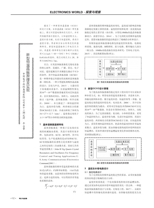
引言:石英晶体振荡器是无线电设备的核心部件,是通信、广播、雷达、电子对抗、遥控遥测及许多测量仪器必不可少的部件,其中恒温晶体振荡器(OCXO )是一种频率稳定性最好的高精密晶体振荡器(蒋松涛,一种小型超低相噪恒温晶振的设计:压电与声光,2015)。
大量应用于高端通讯设备中。
目前温频特性要达到10-9~10-11数量级普遍采用双层恒温技术。
存在预热时间长,体积大,功耗高等缺点(赵声衡,晶体振荡器:科学出版社,2008)。
本文描述了一种恒温控制为主,温度补偿为辅,两者相结合的新型OCXO 设计方案。
并成功研制了体积为36×27×12.7(mm ),温度稳定度优于±1×10⁻⁹的小体积低功耗恒温晶振。
1 晶体谐振器温频特性晶体谐振器是一种基于压电效应实现的机械振动系统。
其晶片切型有很多种,包括AT 切、SC 切、BT 切等。
其中比较常用、生产较成熟的是AT 切和SC 切。
SC 切谐振器的显著特点是其频率与温度之间有近似的三次函数关系,因而它具有零温度系数点(John R.Vig Quartz Crystal Resonators and Oscillators For Frequency Control and Timing Applications:U.S.Army Communications-Electronics Command,2001)。
Ku波段低相噪频率源的研制

Ku波段低相噪频率源的研制周建;张玉兴【摘要】阐述了Ku波段低相噪锁相频率源的研制过程.在低输入参考频率10 MHz的情况下,输出高达11.8 GHz的点频信号,倍频恶化达到61 dB,如何实现从10 Hz~1 MHz频偏范围内各点的相位噪声指标要求是需要攻克的技术难题.具有超低相噪基底的模拟鉴频鉴相器件HMC440的应用为该项目的成功研制奠定了坚实的基础.【期刊名称】《现代电子技术》【年(卷),期】2007(030)023【总页数】3页(P85-87)【关键词】鉴频鉴相器;相位噪声;锁相频率合成器;杂散抑制【作者】周建;张玉兴【作者单位】电子科技大学,电子工程学院,四川,成都,610054;电子科技大学,电子工程学院,四川,成都,610054【正文语种】中文【中图分类】TN9111 引言随着电子技术的飞速发展,目前的电子产品特别是军用产品的工作频段大量地由射频转向微波,Ku、K波段的振荡器、频率合成器、低噪声放大器等已经十分常见。
作为各种电子系统核心部件的频率合成器(简称频综),虽然有着70多年的发展历史,其理论基础可谓相当完善,但仍然受到实际应用的严峻考验。
目前的频率合成器正朝着模块化、小型化、低功耗、高频谱纯度和多点快速捷变的方向发展。
本文研究的频率合成器是工作在11.8 GHz上的一个点频源,其各项技术指标要求如下:输入频率:10 MHz;输入功率:0 dBm;输出频率:11.8 GHz;输出功率:≥7 dBm;杂波抑制:≥65 dBc;谐波抑制:≥40 dBc。
相位噪声如表1所示。
表1 相位噪声要求10 Hz100 Hz1 kHz10 kHz100 kHz1 MHz-60 dBc/Hz-75-95-100-100-110该项目的难点在于:在低参考输入频率(fref=10 MHz)的情况下,输出高达11.8 GHz的点频信号,并且要同时满足10 Hz~1 MHz频偏范围内比较苛刻的相位噪声指标。
频综

● Effect of Frequency Instability Caused by Phase Noise on the Performance of Fast FH Communication System 2004 IEEE ● Effect of RF Oscillator Phase Noise on Performance of Communication System 2004 IEEE ● Local Oscillator Phase Noise and Effect on correlation Millimeter wave Receiver Performance ● Understanding the Effects of Phase Noise in Orthogonal Frequency Division Multiplexing 2001 IEEE 4、相位噪声对OFDM系统性能的影响是当前热门学术话题 、相位噪声对 系统性能的影响是当前热门学术话题 OFDM相关文献举例: 相关文献举例: 相关文献举例 ● Effects of Phase Noise at 60th Transmitter and Receiver on the Performance of OFDM Systems 2006 IEEE ● Compensation of Phase Noise in OFDM wireless Systems 2007 IEEE ● Common Magitude error Due to Phase Noise in OFDM Systems 2007 IEEE
雷达领域相关文献举例: 雷达领域相关文献举例: ● A New Approach for Evaluating the Phase Noise Requirements of STALO in Doppler Radar the 37th European Microwave Conference ● Effects of Transmitter Phase Noise on Millimeter wave LFMCW Radar Performance 2008 IEEE. ● The Effect of Phase Noise in a Stepped Frequency Continuous wave Ground Penetrating Radar 2001 IEEE ● The Influence of Transmitter Phase Noise on FMCW Radar Performance 2006 EuMA ● Prediction of Phase Noise in TWT based Transmitter for a Pulsed Doppler Radar 1996 IEEE
低噪声CMOS图像传感器的研究

C D的概念提出以后 , C 它的潜力被许多科技工作者
h+ ^ .Il … + l*
; m ^ , ^ 1
固体图像传感器技术 , 其中, 最有发展潜力 的是采用 标准 的 C O M S工艺 技 术 来 生产 图像 传 感 器 , 即 C O 图像传感器。 M S CO M S图像传感器的核心部分包括 :光敏感元 电路 、 数字图像处理电路 , 如图 1 所示 。光敏元件感
O i mcn ut ) 晶体管 电荷存储器的基础上 x e e i dc r dS o o 发展起来 的 , 它是一个多栅 MO S晶体管 , 即在源与 漏之 间密 布许多栅极 、沟道极 长的 M S晶体 管 。 O
数转换器 、 精密放大器 、 存贮器 、 运算单元等元件的 功能 。问题之二是 C D阵列驱动脉 冲复杂, C 需要使
【】 集 成 电 路 l国
■●_
C hi a It gr t d Ci ui n n e a e r t c
设 计
一 。
低噪声 CMOS图像传感器的研究
王 旭 , 成 刘
摘要: 近年来 CO M S图像传感器在 医疗和工业 C 等领域 中得到了越 来越广泛的应用 。作 为 C O T M S图像传
8 年代 中期 , 0 基于这三种 固体 图像 传感器技术 的工
ห้องสมุดไป่ตู้
业和民用产品逐渐投放市场 。在这三种固体图像传 单元阵列难与驱动电路及信号处理电路单片集成 , 感器 中 ,C C D发展 最 为迅速 。 C C D是 在 MO Me l S( t 不易处理一些模拟和数字功能 ,这些功能包括模 / a
优美斯(Optimax Systems)的相位平移干扰光学测量方法白皮书说明书

The Effect Of Phase Distortion On InterferometricMeasurements Of Thin Film Coated Optical SurfacesJon Watson, Daniel SavageOptimax Systems, 6367 Dean Parkway, Ontario, NY USA*********************©Copyright Optimax Systems, Inc. 2010This paper discusses difficulty in accurately interpreting surface form data from a phase shifting interferometer measurement of a thin film interference coated surfaces.PHASE-SHIFTING INTERFEROMETRYPhase-shifting interferometry is a metrology tool widely used in optical manufacturing to determine form errors of an optical surface. The surface under test generates a reflected wavefront that interferes with the reference wavefront produced by the interferometer 1. A phase-shifting interferometer modulates phase by slightly moving the reference wavefront with respect to the reflected test wavefront 2 . The phase information collected is converted into the height data which comprises the surface under test3.Visibility of fringes in an interferometer is a function of intensity mismatch between the test and reference beams. Most commercially available interferometers are designed to optimize fringe contrast based on a 4% reflected beam intensity. If the surface under test is coated for minimum reflection near or at the test wavelength of the interferometer, the visibility of the fringe pattern can be too low to accurately measure.OPTICAL THIN-FILM INTERFERENCE COATINGSOptical thin-film interference coatings are structures composed of one or more thin layers (typically multiples of a quarter-wave optical thickness) of materials deposited on the surface of an optical substrate.The goal of interference coatings is to create a multilayer film structure where interference effects within the structure achieve a desired percent intensity transmission or reflection over a given wavelength range.The purpose of the coating defines the design of the multilayer structure. Basic design variables include:• Number of layers• Thickness of each layer• Material of each layerThe most common types of multilayer films are high reflector (HR) and anti-reflection (AR) coatings. HR coatings function by constructively interfering reflected light, while AR coatings function by destructively interfering reflected light. These coatings are designed to operate over a specific wavelength range distributed around a particular design wavelength.To produce the desired interference effects, thin-film structures are designed to modulate the phase of the reflected or transmitted wavefront. The nature of the interference effect depends precisely on the thickness of each layer in the coating as well as the refractive index of each layer. If the thickness and index of each layer is uniform across the coated surface, the reflected wavefront will have a constant phase offset across the surface. However, if layer thicknesses or index vary across the coated surface, then the phase of thereflected wavefront will also vary. Depending on the design of the coating and the severity of the thickness or index non-uniformity, the distortion of the phase of the reflected wavefront can be severe. 4Layer thickness non-uniformity is inherent in the coating process and is exaggerated by increasing radius of curvature of the coated surface.5 All industry-standard directed source deposition processes (thermal evaporation, sputtering, etc) result in some degree of layer thickness non-uniformity.5 Even processes developed to minimize layer non-uniformity, such as those used at Optimax, will still result in slight layer non-uniformity (within design tolerance).TESTING COATED OPTICS INTERFEROMETRICALLYPhase-shifting interferometers use phase information to determine the height map of the surface under test. However, surfaces coated with a thin-film interference coating can have severe phase distortion in the reflected wavefront due to slight layer thickness non-uniformities and refractive index inhomogeneity. Therefore, the measured irregularity of a coated surface measured on a phase shifting interferometer at a wavelength other than the design wavelength, may not represent the actual irregularity of the surface. Even using a phase shifting interferometer at the coating design wavelength does not guarantee accurate surface irregularity measurements. If a coating has very low reflectance over any given wavelength range (such as in the case of an AR coating), the phase shift on reflection with wavelength will vary significantly in that range.7 Figure 1 shows an example of how the phase can vary with coating thickness variations.Figure 1In this particular case, if a point at the lens edge has the nominal coating thickness and the coating at lens center is 2% thicker, expect ~38° phase difference in the measurement (~0.1 waves). This will erroneous be seen as height by the interferometer, despite the actual height change in this case being less than 7nm (~0.01 waves). Also, depending on coating design, low fringe visibility may inhibit measurements.There is an extreme method to determine the irregularity of a thin-film interference coated surface by flash coating it with a bare metal mirror coating. A metal mirror coating is not a thin-film interference coating, and the surface of the mirror represents the true surface, This relatively expensive process requires extra time, handling, and potential damage during the metal coating chemical strip process.CONCLUSIONS•There can be practical limitations to getting accurate surface form data on coated optical surfaces due to issues with phase distortion and fringe visibility.•The issues are a function of thin film coating design particulars and the actual deposition processes.1 R.E. Fischer, B. Tadic-Galeb, P. Yoder, Optical System Design, Pg 340, McGraw Hill, New York City, 20082 H.H. Karow, Fabrication Methods For Precision Optics, Pg 656, John Wiley & Sons, New York City, 19933 MetroPro Reference Guide OMP-0347J, Page 7-1, Zygo Corporation, Middlefield, Connecticut, 20044 H.A. Macleod, Thin Film Optical Filters, Chapter 11: Layer uniformity and thickness monitoring, The Institute of Physics Publishing, 2001.5 R.E. Fischer, B. Tadic-Galeb, P. Yoder, Optical System Design, Pg 581, McGraw Hill, New York City, 2008。
恒温晶体振荡器相关知识介绍

1 恒温晶体振荡器基本原理恒温晶体振荡器简称恒温晶振,英文简称为OCXO(Oven Controlled Crystal Oscillator),是利用恒温槽使晶体振荡器中石英晶体谐振器的温度保持恒定,将由周围温度变化引起的振荡器输出频率变化量削减到最小的晶体振荡器。
OCXO是由恒温槽控制电路和振荡器电路构成的。
通常人们是利用热敏电阻“电桥”构成的差动串联放大器,来实现温度控制。
恒温晶振的基本结构见图1。
2 恒温晶体振荡器的应用领域1)军事和宇航领域:通讯导航、敌我识别器、雷达、传感器、制导系统、引信、电子战、声纳;2)科研与计量:原子钟、测量设备、遥测、遥感、遥控;3)工业领域:通讯、电信、移动/蜂窝/便携式终端、航空、航海、导航、仪器仪表、计算机、数字设备、显示器、磁盘驱动器、调制解调器、标识/认证系统、传感器;4)消费领域:手表与时钟、蜂窝与无绳电话机、普通电话机、呼叫器、音响设备、有线电视系统与电视机、PC、摄象机、业余无线电器材、玩具、医用装置与设备;5)汽车领域:引擎控制,立体声音响时钟,传感器,驾控计算机,GPS应用。
3 恒温晶体振荡器专业术语1)频率准确度:按规定条件要求,在基准温度下测试,晶体振荡器的频率相对于其规定标称值的最大允许偏差,即(f-f0)/f0;2)频率-温度稳定度:按规定条件要求,在规定温度范围内晶体振荡器输出频率的最大变化量相对于温度范围内输出频率极值之和的允许频偏值,即±(fmax-fmin)/(fmax+fmin);3)频率老化:晶体振荡器输出频率随时间的变化,通常用某一时间间隔的频率来量度。
如0至30天的总变化或1年内的预定总频率变化等;4)工作温度范围:振荡器能正常工作。
其频率及其他性能均不超过规定的允许偏差的温度范围;5)稳定时间:振荡器从初始加电到稳定工作在规定极限值所需要的时间;6)相位噪声:是指信号功率与噪声功率的比率(C/N),是表征频率颤抖的技术指标。
博威集成电路 集成晶体振荡器目录 说明书
晶振电路的生产研发条件质量保证命名规则恒温晶体振荡器(OCXOs)OX253B-H-MR-V-10M OX362D-H-MR-V-10MOX20系列10~40SC±0.01~0.20.2S/T/HOX30x系列10~120SC±0.005~0.20.5S/T/H-140/-14556●●9●1215订购表7●OX14B-T-HU-V-10MOX12A-T-HT-V-40M温度补偿晶体振荡器(TCXOs)TX12/TX14/TX15系列10~120±0.5~512/5/3.3S/T/H/CTXG36B-S-KW-R@300M1922命名规则●-55~+85CTX7A-C-GU-V@10M TX12B-T-JW-N@20M注:ppm=10,120MHz以上为倍频输出,可选定制产品;10MHz以下为分频输出;产品概览8●型号频率范围f(MHz)频率温度稳定度压控频率范围工作电压V输出选择*电压控制晶体振荡器(VCXOs)ppmVX12/VX14/VXM14(SMD)ppm压控线性注:ppm=10, 除VXM15系列外,频率>35MHz压控频率范围为±30ppm; 需宽压控频率范围可选倍频输出。
*:S:Sinewave; LC:L VCMOS; LP:LVPECL。
VXM15B-T-HQ-A@100M页码24命名规则●VX12/VX14/VXM14集成晶体振荡器目录封装外形尺寸图35(TMs )±ppmppm时钟模块概述VTM18B-T-HT-001页码TM18系列±4.62/2CMOS5/3.328±0.370.008~32.768●27集成晶体振荡器目录(XTALs )封装页码29命名规则●±5ppm1、完善的晶体谐振器生产线2 我们拥有1000m 资上千万元完整的晶体谐振器生产线,其主要设备从国外引进,可生产高Q、低老化冷压焊和电阻焊(抽真空)SC、AT切晶体。
gps时钟驯服晶振在南京大学成功案例
gps时钟驯服晶振在南京大学成功案例2017年10月初,西安同步电子科技有限公司自主研发生产的gps 时钟驯服晶振在南京大学投入使用,这套驯服晶振已稳定运行数月,已将我公司纳为合格供应商。
一、时钟驯服晶振简介时钟驯服的基本原理是利用卫星授时接收机提供的固定频率信号,与本地振荡器产生的振荡信号进行比对,获得频率差;再通过对本地振荡器的调节,使振荡频率与卫星的振荡频率基本一致,在频率调整过程中,还需要对本地振荡器的相位进行补偿,使本地振荡器输出的分频秒信号与接收机输出的秒信号差值在一定范围内.卫星授时接收机由于信号传输距离长,易受干扰等特点,其输出的1pps 具有一定的抖动,秒信号包含多种误差成分,如:卫星时钟误差:星历误差:电离层的附加延时误差:对流层的附加延时误差:多路径误差:接收机本身的误差。
采用GPS授时接收机对高稳晶振进行升级改造,研制高精度时间间隔计数器电路,测量GPS平均秒和高稳晶振分频秒之间的时差,采用驯服算法计算晶振的实时准确度,并通过电子频率控制的方式反馈调整高稳晶振的频率信号,从而提高频率信号的准确性和稳定性。
二、GPS驯服晶振利用高精度的时间间隔测量方法测得GPS信号和本地秒信号的相位差,并经计算机处理后转换成频率差,然后通过高稳晶振的压控调谐对高稳晶振输出频率进行调整,由锁相环回路进行控制使高稳晶振锁定到GPS时钟的准确度,从而完成对高稳晶振的驯服校频过程。
对输入本地频标和GPS秒脉冲信号的鉴相,通过高精度时间间隔测量,测量出两信号的相位差,并将转换为电压值。
然后通过压控OCXO端口对高稳晶振进行压控调整,通过锁相环使本地频标锁定到GPS时钟上。
影响误差分析其中主要影响是GPS引入误差。
又可分为以下几方面的误差:1.1与GPS卫星相关的误差1.1卫星星历误差卫星星历误差是指卫星星历给出的卫星空间位置和卫星实际位置间的偏差,由于卫星空间位置是由地面监控系统根据卫星测轨结果计算求得的,所以又称为卫星轨道误差。
vco 相位噪声相关频率
vco 相位噪声相关频率VCO相位噪声相关频率VCO(Voltage Controlled Oscillator)是一种电压控制振荡器,常用于无线通信系统中的频率合成器。
在实际应用中,VCO的性能参数之一是相位噪声,它对通信系统的性能有着重要影响。
相位噪声是指VCO输出信号相位的随机变化,它与频率有一定的关系,即相位噪声相关频率。
相位噪声的相关频率是指相位噪声随频率变化的规律。
在VCO中,相位噪声一般由噪声源引起,噪声源包括各种器件的热噪声、1/f 噪声等。
这些噪声源会对VCO的输出信号相位产生影响,从而导致相位噪声的存在。
相位噪声的相关频率可以通过功率谱密度来表示。
功率谱密度是将相位噪声的能量在频率上的分布进行描述的一种方式。
对于VCO而言,相位噪声的功率谱密度通常被建模为一个随频率增加而增加的函数。
具体来说,VCO的相位噪声功率谱密度可以分为两个部分:高频段和低频段。
在高频段,相位噪声功率谱密度随频率的增加而增加。
这是由于VCO中的噪声源所引起的高频噪声对相位噪声的贡献较大。
而在低频段,相位噪声功率谱密度随频率的减小而减小。
这是由于1/f噪声等低频噪声对相位噪声的贡献较大。
在VCO设计和应用中,相位噪声相关频率是一个重要的参数。
它可以用来评估VCO的性能,并对VCO在无线通信系统中的应用进行优化。
相位噪声相关频率越低,意味着VCO在更低的频率范围内具有较好的相位噪声性能。
这对于要求高稳定性和低相位噪声的通信系统来说尤为重要。
为了降低VCO的相位噪声相关频率,可以采取一些措施。
例如,优化VCO的电路结构,减小噪声源的影响;改善VCO的供电和接地结构,减少电源噪声对VCO的干扰;采用合适的滤波器和稳压电路,降低噪声在VCO电路中的传播和放大等。
这些措施可以有效地降低VCO的相位噪声相关频率,提高VCO的性能。
VCO的相位噪声相关频率是评估VCO性能的重要指标之一。
它对于无线通信系统的稳定性和性能有着重要影响。
Agilent N9010A EXA 信号分析仪 说明书
设置为 normal(正常),则分析 仪必须开机至少 30 分钟;如果 “Auto Align”设置为 off(关闭) 或partia(l 部分),则必须在足够 近的时间内进行过校正,以避免 出现告警信息。如果“告警”条 件从“时间和温度”变成禁用的 时间长度选择之一,则分析仪可 能达不到技术指标,并且不会向 用户发出通知。
Agilent N9010A EXA
信号分析仪
技术资料
可用的频率范围 N9010A-503 N9010A-507 N9010A-513 N9010A-526
9 kHz~3.6 GHz 9 kHz~7.0 GHz 9 kHz~13.6 GHz 9 kHz~26.5 GHz
LXI C 类标准认证
目录
定义与条件 .............................. 3
9 kHz~3.6 GHz 3.5~7.0 GHz 6.9~13.6 GHz 13.5~17.1 GHz 17~26.5 GHz
频率基准 精度 老化率
温度稳定性 20~30℃ 5~50℃
可获得的最初校准精度
最后一次调整后 1 年内的频率 基准精度示例(包括选件 PFR) 剩余 FM(调频)
选件 PFR 标准
一般技术指标 ......................... 11
温度范围 ................................... 11 EMC .......................................... 11 安全 ........................................... 11 音频噪声 ................................... 11 环境强化测试 ........................... 11 电源要求 ................................... 12 数据存储 ................................... 12 重量 ........................................... 12 尺寸 ........................................... 12 保修 ........................................... 12 校准周期 ................................... 12
- 1、下载文档前请自行甄别文档内容的完整性,平台不提供额外的编辑、内容补充、找答案等附加服务。
- 2、"仅部分预览"的文档,不可在线预览部分如存在完整性等问题,可反馈申请退款(可完整预览的文档不适用该条件!)。
- 3、如文档侵犯您的权益,请联系客服反馈,我们会尽快为您处理(人工客服工作时间:9:00-18:30)。
• Achieving measurement accuracy in a reasonable amount of time at offset points close to the carrier
• Reaching the noise floor farther away from the carrier.
After a lengthy and thorough investigation it turned out that the spurious “bumps” at 100 KHz, 700 KHz, and 900 KHz offsets from the carrier were caused by mixing the broadcast signals from the local FM radio stations (at 100.1 MHz, 100.7 MHz, 99.1 MHz) with 100 MHz OCXO signal. While testing good, but not ULPN 100 MHz devices, (which have noise floor at -170 dBc/Hz or higher), this phenomenon is hardly noticeable. Therefore this challenge is specific to ULPN OCXO with a phase noise floor around -180 dBc/Hz, particularly running at 100 MHz, especially in urban areas, where the power from the FM stations is quite high. If the
As expected, the measured phase noise far from the carrier was improved by 3 – 5 dB, while discrepancies in results from a few KHz offset in were not very noticeable. Realizing that the phase noise on the noise floor is determined by the circuit, and for given design unit to unit variations are negligible, the instrument of choice still would still be 5120A-01, however, during the design qualification stage, the verification of the noise floor values on the DCNTS is required.
For higher frequency ULPN OCXO, specifically at 100.000 MHz carrier frequency, RF pollution in the environment, and EMI added further challenges.
For devices, which employ a phase lock loop (PLL) technique for attaining higher frequency the interaction of the device PLL and test instrument’s PLLs made it even more difficult to achieve accurate results.
Fig.1. 10 MHz ULPN OCrn was the resolution (noise floor) of the measurement at large offsets from the carrier (the noise floor of the device). The instrument’s specification calls (conservatively) for -168 dBc/Hz floor at offsets greater than 10 KHz. The theoretical expectations were closer to -175 dBc/Hz at 100 KHz offsets and beyond. We decided to verify our expectations with a Noise XT Dual Core Noise Test Set (DCNTS) [2], [4]. It is a considerably more difficult type of test. It requires two references with similar performance as the DUT (the better the references’ performance – the faster the test), the references must have voltage control (ability to change frequency with the change of the voltage on the control terminal), and be calibrated exactly on the frequency of DUT. The test result of the same device is shown in Fig.2.
Fig. 3. 100 MHz ULPN OCXO with “bumps” caused by RF pollution.
frequency is far away from the broadcasting FM band, this phenomenon doesn’t occure. In order to improve this condition we took several measures:
TESTING PHASE NOISE OF ULTRA LOW PHASE NOISE OCXO – CHALLENGES AND SOLUTIONS
Roman Boroditsky, Jorge Gomez
NEL Frequency Controls Burlington, WI USA
romanb@ gomezj@
1. Accuracy
2. Repeatability
3. Speed of test
4. Ease of use
5. Range
6. Cost
7. Ease of data retrieval
The value of each characteristic also depends on whether the test is intended for use in production environment, or in the lab. The “two oscillator method” [1] was ruled out, since it does not satisfy the first four criteria very well, and therefore only methods and equipment, employing cross-correlation technique were considered. [1], [4]. The challenges for lower frequency devices (around 10.000 MHz) were :
Abstract—Modern instrumentation equipment, commercial & defense communication systems, and radar equipment require excellent stability, extremely low phase noise frequency sources. Testing devices that exhibit phase noise of -120 dBc/Hz at 1 Hz offset from the carrier and better than -180 dBc/Hz on the noise floor is a challenge using existing test equipment and methods. It is especially pertinent to production environment, where measurement time and accuracy of each measurement becomes critical. The purpose of this work was to investigate different test methods, evaluate different phase noise measurement equipment, and find acceptable solutions for both low frequency (around 10 MHz) Ultra Low Phase Noise (ULPN) reference, and HF/UHF ULPN OCXO. Several test methods and test instruments were investigated. There’s no “one size fits all” solution, but for each frequency range the optimum solutions were proposed.
Introduction, Challenges