OB2532_Demo Board Manual(15W)_
OB2532中文数据手册
kHz % V dB uA V V V nS nS
误差放大器部分
INV=2V,Comp=0V
VDD=16V,Io=20mA VDD=16V,Io=20mA
门驱动输出部分 VOL VOH V_clamp T_r T_f
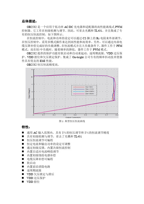
注意:1、Freq_Max 表示 IC 内部的最大时钟频率。在系统应用中,60KHz 额定的最大工作 频率存在于最大输出功率或是恒压到恒流的转变点。
WW:周编号(01-52)
S:网络编号(可选的)源自引脚分配引脚号 1 2 3 4 5 6 引脚名 GND GATE CS INV COMP VDD I/O P O I I I P 描述 地 图腾柱门级驱动输出,驱动功率 MOSFET 电流检测输入,连接 MOSFET 电流检测电阻端 从辅助绕组来的电压反馈。连接到电阻分压器,反应输出电压 变化。占空比由误差放大器的输出和 3 脚的电流检测决定。 恒压稳定性的环路补偿 供电电源
应用
低功率 AC/DC 离线式开关电源用于 手机充电器 数字摄像机充电器 小功率适配器 个人电脑、电视等的辅助电源 线性调节器/RCC 替代 OB2532 提供 SOT23-6 封装
典型应用
一般信息
引脚结构 SOT23-6 封装引脚图如下所示
定购信息 器件号 OB2532MP
描述 SOT23-6,Pb-free,T&R
I_COMP_MAX
INV=0V,Comp=5V 频率抖动范围 EA 的参考电压 EA 的直流增益 最大电缆补偿电流 输出最低电平 输出最高电平 输出拑位电压电平 输出高电平时间 输出低电平时间
VDD=16V,CL=0.5nF VDD=16V,CL=0.5nF
14 +/-4 1.97 2 60 28 1 8 16 700 35 2.03
ISD2532P资料
•
• • • • • • • •
-2-
ISD2532/40/48/64
3. BLOCK DIAGRAM
Internal Clock XCLK
Timing
Sampling Clock ANA IN Amp 5-Pole Active Antialiasing Filter Decoders Analog Transceivers 256K Cell Nonvolatile Multilevel Storage Array
VCCA
VSSA VSSD VCCD
A0 A1 A2 A3 A4 A5 A A7 A8PDOVF
P/R
CE
EOM
AUX IN
-3-
Publication Release Date: April 24, 2006 Revision 1.2
ISD2532/40/48/64
4. TABLE OF CONTENTS
1. GENERAL DESCRIPTION.................................................................................................................. 2 2. FEATURES ......................................................................................................................................... 2 3. BLOCK DIAGRAM .............................................................................................................................. 3 4. TABLE OF CONTENTS ...................................................................................................................... 4 5. PIN CONFIGURATION ....................................................................................................................... 5 6. PIN DESCRIPTION ............................................................................................................................. 6 7. FUNCTIONAL DESCRIPTION.......................................................................................................... 10 7.1. Detailed Description.................................................................................................................... 10 7.2. Operational Modes ..................................................................................................................... 11 7.2.1. Operational Modes Description............................................................................................ 12 8. TIMING DIAGRAMS.......................................................................................................................... 16 9. ABSOLUTE MAXIMUM RATINGS.................................................................................................... 19 9.1 Operating Conditions ................................................................................................................... 20 10. ELECTRICAL CHARACTERISTICS ............................................................................................... 21 10.1. Parameters For Packaged Parts .............................................................................................. 21 10.1.1. Typical Parameter Variation with Voltage and Temperature - Packaged Parts ................ 24 10.2. Parameters For Die .................................................................................................................. 25 10.2.1. Typical Parameter Variation with Voltage and Temperature - Die .................................... 28 10.3. Parameters For Push-Button Mode.......................................................................................... 29 11. TYPICAL APPLICATION CIRCUIT ................................................................................................. 30 12. PACKAGE DRAWING AND DIMENSIONS .................................................................................... 35 12.1. 28-Lead 300-Mil Plastic Small Outline IC (SOIC)..................................................................... 35 12.2. 28-Lead 600-Mil Plastic Dual Inline Package (PDIP) ............................................................... 36 12.3. Die Bonding Physical Layout [1] ................................................................................................ 37 13. ORDERING INFORMATION........................................................................................................... 39 14. VERSION HISTORY ....................................................................................................................... 40
基才OB2532的原边反馈LED驱动电路设计
Ke y wo r d s :L ED;p i r ma r y - s i d e f e e d b a c k;p u l s e - w i d t h mo d u l a t i o n;OB2 5 3 2
L E D照 明 因 其 节 能 、 环保 和寿命 长等特 点 . 成 为 未 来 照 明 的 发 展 趋 势 。L E D 灯 不 像 普 通 的 白炽 灯 泡 , 可 以 直 接 连 接 2 2 0 V 的交 流市 电 , 它需 要 低 压 直 流 驱 动 , 因 此 必 须 设 计 复 杂 的 电 源 变 换 电路 。 I 压D 的寿 命 和 驱 动 电源 有 很 大 的关 系【 1 】 . 驱 动 电 源供 电不 稳定 , 导致 L E D发 光 效 率 降 低 , 寿命 缩 短 , 颜 色
Z HANG T a o ,Z HAN G Xi a n — z h o n g
( c 0
o fI n f o r m a t i o n S c i e n c e a n dE n g i n e e r i n g , Wu h a n U n w e  ̄ o fS c i e ce n a n d T e c h n o l o g y ,Wu h a n 4 3 0 0 8 1 , C h i n a )
到 设 计 要 求
关键词 : 发 光 二 极 管 :原 边 反 馈 ; 脉 宽调 制 ;O B 2 5 3 2
中图分类号 : T N 8 6 文献标识码 : A 文 章 编 号 :1 6 7 4 — 6 2 3 6 ( 2 0 1 3 ) 2 2 — 0 1 0 5 — 0 3
OB2538_Demo board_Manual_(12W)

Revision Historyri g ht co n f i d裕创otlaitnBottomBottomTop2.4. Adapter Module SnapshotOn -B ri g ht co n f i de to创裕Winging Start RemarkN1 0.21N2 0.21TAPE TAPE W=12mm (Y) 2 N3 Copper 12mm 2 1.1 TAPE TAPE W=12mm (Y)8 N4 0.50 Φ*1 triple insulated wire16 TAPE TAPE W=12mm (Y) 2 N5 0.20*3 2UEW TAPE TAPE W=12mm (Y) N6 0.18*3 2UEW 19 TAPETAPE W=12mm (Y)3n -B ri g ht co n f i de n264Vac/50HZ 14611.860Fig. 1 No-load Input Power vs. Input Line Voltage3.1.2. Efficiency25% 50% 75% 100% Aver. Eff. 115Vac/60HZ 79.88 80.74 80.49 79.60 80.17230Vac/50HZ 78.3280.50 80.7280.4079.98Fig. 2 Efficiency vs. Percent of Rated Output Powerg ht co n f i de nt i a l to创Fig. 3 Measured ripple& noise waveform@90Vac/60HZ, no loadFig. 4 Measured ripple& noise waveform@90Vac/60HZ, full loadOn -B ri g ht co n fFig. 5 Measured ripple& noise waveform@264Vac/50HZ, no load Fig. 6 Measured ripple& noise waveform@264Vac/50HZ, full load3.2.3. Over Shoot & Under ShootOver shoot and under shoot were measured under below conditions. a. AC input switch on for over shoot and off for under shoot. b. Input voltage ranges from 90Vac/60HZ~264Vac/50HZ. Table. 5 Over shoot & under shoot measurement resultsInput loadRemark over shoot Fig. 8 Full loadFig. 8 Measured overshoot waveform@90Vac/60HZ, no loadOn -B ri g de nt i a l to创裕Fig. 10 Measured overshoot waveform@264Vac/50HZ, no loadA dynamic loading with low set at 20% load lasting for 50ms and high set at 80% load lasting for 50mS is -B ri g ht co n to创裕Fig. 13 Turn on delay time measured waveform @100Vac/60HZ,full loadFig. 14 Turn on delay time measured waveform @240Vac/50HZ,full loadFig. 15 Hold-up time measured waveform@100Vac/60HZ,full loadFig. 16 Rise time measured waveform@100Vac/60HZ,full loadOn -B ri g ht co n f i de nt i a l toFig. 19 Fall time measured waveform@240Vac/50HZ,full load-B ri g ht co n f i de创裕On -B ri g ht co n f i de nt i a l to创裕n -B ri g ht co n f i de nt i a l to创裕3.3.2.2. FCC CLASS B @ full load reportOn -B ri g ht co n f i de nt i a l to创裕removed.Fig. 20 Output short, Vdd 、Cs 、Vds waveform@90 Vac/60Hz, full load Fig. 21 Output short, Vdd 、Cs 、Vdd waveform@264 Vac/50Hz, full load4.3. Open Loop ProtectionTable. 9 OLP @ Full loadInput OLP Protection115Vac/60Hz OK 230Vac/50Hz OK4.4. Over Current ProtectionTable. 10 Over current ProtectionInput OCP Current OCP Recovery g ht co n f i de nt i a l to创裕创otlaitnFig. 22 Vdd, Sense&Vds waveform@90Vac/60Hz,no load Fig. 23 Vdd, Sense & Vds waveform @90Vac/60Hz, full loadFig. 24 Vdd, Sense & Vds waveform @264Vac/50Hz, no loadFig. 25 Vdd, Sense & Vds waveform @264Vac/50Hz,full load 6.2. MOSFET Vdd 、Cs 、Vds waveform @ start /output shortOn -B ri g ht co n f i de nt i a l to创裕Fig. 31 Output short, Vdd 、Cs 、Vds waveform@90 Vac/60HzFig. 32 Output short, Vdd 、Cs 、Vds waveform@264 Vac/50HzTable. 10 Vds_max @ Full load / Output shortInputVds_max(V)264Vac/50Hz @No load500 264Vac/50Hz @ Full load550 264Vac/50Hz @ Output short500B ri g ht co n f i de nt i a l t创裕。
OB2532A Datasheet_CN_佛山照明_111209

定购信息 型号 OB2532AMP
备注: 芯片的实际应用条件超出规定的“应用极限值”将会 对芯片造成永久性损伤。以上应用极限值标志了芯片可承 受应力等级, 但并不建议芯片在此极限条件或超出“推荐工 作条件”下工作。 芯片长时间处于最大额定工作条件, 会影 响芯片的可靠性。
lt
o
佛
应用极限参数 Parameter VDD 电压 VDD 稳压管钳位电流 COMP 电压 CS 输入电压 INV 输入电压 最小/最大工作结温 TJ 最小/最大储藏温度 Tstg 管脚焊接温度(10secs)
佛
40 80 Temperature(℃)
山 照
120
明
OB2532A
高精度原边 PWM 电源开关器
工作原理概述
OB2532A 是一款低系统成本的 LED 驱动控制 器,芯片工作在不连续(DCM)模式,应用于反 激隔离 LED 照明。采用原边反馈控制技术,无 需 TL431 和光耦等二次侧元器件, 其内置专利的 恒流(CC)控制技术,可以实现高精度的 LED 恒流输出特性,满足 LED 照明应用。 启动电流和启动控制 OB2532A 优化设计了启动电流(Typ. 5uA) ,当 VDD 电压经充电高于 UVLO(OFF)阈值电压, 芯片可以很快开启工作,因此在系统板上可以使 用高阻值的启动电阻来减小功率损耗。 工作电流 OB2532A 低至 2mA 的工作电流和多模式控制方 式可以实现系统的高转换效率和低待机功耗。 软启动 系统上电后,OB2532A 的内部软启动功能可以 减小 LED 电流过冲, 当 VDD 电压经充电高于 UVLO(OFF)阈值电压,芯片内部算法控制 CS 引脚峰值电压逐渐从 0V 增加到 0.8V,每次重启 都有软启动。 CC 工作原理 OB2532A 专利的 CC 控制需要工作在不连续模 式,应用于反激隔离 LED 照明(参考第 1 页典型 应用图)。LED 输出电流 Iout 计算公式: TDemag 与原边绕组电感量成反比例,控制 Lp 和开 关频率的乘积恒定不变,这样输出电流就不随原边 电感量的变化而变化。 芯片最大补偿原边电感量± 7% 偏差变化,实现 LED 恒流输出。 LED 输出电流计算公式:
YD2512英文说明书

Table of ContentsCHAPTER1: Overview1. Introduction (2)2. Technical Index (2)3. Operating Environment (3)CHAPTER 2: Instrument Structure1. Front Panel Instruction (3)2. Rear Panel Instruction (4)CHAPTER3: Operation Instruction1. Conventional Test (5)2. Parameter Setup (6)1 R Value Direct-Read Mode Setup (6)2 △%Read Mode Setup (6)3 Sorting Setup (7)4 Clear Setup (7)5 Alarm Setup (7)6 Speed Setup (7)7 External Trigger Setup (7)8 Serial Communication Setup (7)3. Example (8)Chapter4: Packing and Warranty1. Packing (10)2. Warranty (10)Chapter 1: Overview1. Product IntroductionYD2512 DC is intelligent DC Low-ohm meter with wide measurement range and high-accuracy. It can be used to measure resistance of transformer, electric engine, switch, relay, connector contact, etc.The measurement range is 1u Ω-1.9999M Ω.The high-accuracy constant current thatinstrument produces through DUT (under test device) will carry on four terminal measurement, which removes leader error effectively and suits user to make the high-accuracy measurement; It is especially suitable to all kinds of tra nsformer and inductance‟s copper measurement; The resistance reading straightly displays High/low-limit and +/- percentage error value, and all setup judgment is for entire range. The percentage error may maximum display ±99.99%, minimum ±0.000%, which enhances instrument‟s application range. Besides, test speed (Fast, Slow) changing, total state and total setup value power-off protection ,etc all make it easier for user to test the product..2. Technical Index1,Display Mode: High-brightness display (VFD )2, Test speed: Slow: 5 Fast: 10 (times/second)3,Read Mode: R value direct-read and △% read4, Measurement Range and each range's Basic Accuracy RangeMeasurement Range Resolution Current Accuracy 20m Ω1u Ω~19.999m Ω 1u Ω 1A ±0.1%+3digits 200m Ω10u Ω~199.99m Ω 10u Ω 100mA ±0.05%+3 digits2Ω100u Ω~1.9999Ω 100u Ω ±0.03%+2 digits 20Ω1m Ω~19.999Ω 1m Ω 10mA 200Ω10m Ω~199.99Ω 10m Ω 1mA 2K Ω100m Ω~1.9999K Ω 100m Ω 100uA 20K Ω1Ω~19.999K Ω 1Ω 10uA 200k Ω10Ω~199.99K Ω 10Ω ±0.05%+3 digits 2M Ω 100Ω~1.9999M Ω 100Ω 1uA ±0.1%+3 digits 5, Range Selection: Auto or Lock6, Trigger Mode: Internal and External trigger Test7,Sorting Signal: Pass, High, Low(online-test)Pass, Fail(Single-test)7, Exterior Size and Weight:Dimension: 290mmX110mmX350mmWeight: Approx.5kg3. Operating Environment:1,Power Supply: AC 50Hz 220V±5%2,Temperature:18~28℃, RH≤80%To guarantee measurement accuracy or not to damage instrument, pay attention to the following items:1. Please do not put the instrument in the environment of multi-dusts, multi-vibrations, straightsunshine or corrosion gas condition when use.2. Although the instrument has dealt with AC current noise, it's better place and use it in lowernoise environment. If can not avoid, please add power filter for instrument.The instrument should be operated in temperature form 0℃~30℃.Package the instrument well if not use for long time.Chapter 2: Panel1. Front Panel Schematic and Function Specification:Display Screen Graph:Graph 2-1Key Area Graph:Graph 2-2Graph 2-3Function Description:1、Test Line Socket(Graph 2-3):Connect four terminal test lines.2、Power Switch: Switch condition depends on makings in the key.3、Display Screen Graph(Graph2-1):Display company brand, test data or unit, setup data or unit,sorting results, setup interface etc.4、Key Area(Graph2-2):(1)Number key: Input setup value directly, range value, code etc.(2)Function Key:Sorting Key: Turn on(COMP lights)or Turn off(COMP disappears)Speed Key: Select slow(Display ‘S’)test or Fast(Display‘F’)TestAlarm Key: Select Pass, Fail Alarm/Alarm turn offLock Key: Test Unit lock or Auto(‘AUTO’Highlights)Display Key: Select R(Display‘R’)or△%(Display‘△%’)Zeroing Key:If necessary, clear test base number to enhance test accuracySetup Key: Enter setup interface or calibration keyEnter Key: Input data to confirmR232 Key: Turn on or off Serial communicationTrigger Key: Select external trigger(EX TRIG Highlights)or internaltriggerNote: Details on Display Graph please contrast Display Screen Indicator2. Rear Panel:Function Description:1, Power Socket: 220V 50Hz 1A2, Handler: PLC Interface3, RS-232C: Serial Interface4, Grounding Protection TerminalChapter3: Operation Instruction1. Conventional TestAfter preheating 20 minutes, connect test jig. Press “Clear "key to make test jig short circuit. To carry on Low-ohm high-accuracy test, do as Graph3—1 to short circuit.图3—1 High-Accuracy Short-circuitTest jig must be in the same side, short circuit bar uses 10 X 5 X 3 red copper or other fine electric conduction material, and the jig should be as near as possible. The jig should not be turned arbitrarily in regular measurement.When doing single-piece measurement, after the instrument tripped stop automatically, then read data after choosing the right range. When measuring with a breed and the first product, press “Display”key to lock in the suitable range after data is stable. It can improve measurement speed.2. Parameter Setup1, R Value Direct-Read Mode Setup1.1 Press“Display” key to select R value in measurement state. Display screen displays ‘R’,High,low-limit resistance setup value and sorting ‟s range setting value.1.2 Press “Setup” key to enter setup state. Display screen displays ‚-Pro-‛.1.3 Press “Setup” key to enter sorting range setup state. When‘RANGE’flashes, now throughNumber key, select test range in need.1~9 respectively represents20mΩ,200mΩ,2Ω,20Ω,200Ω,2KΩ,20KΩ,200KΩ,2MΩmeasurement range. After selecting range, high, low-limit decimal and unit will be fixed, which can not modify in high, low-limit setup.1.4 P ress “Setup” key to enter resistance high-limit setup state. On display screen ‘HIGH’highlights, ‘LOW’disappears, and value after‘HIGH’begins to flash, which shows setup of high-limit nominal value. Display‚×××××‛the first value in the left flashes .Note: X Represents Any Value1.5 Press‘Enter’key to select flash range, then input setup data through Number key. Keeppressing‘Enter’key can make flash range cycle. If do not need modify data, enter next step directly.1.6 Press “Setup” key to enter resistance low-limit setup state. On display screen ‘LOW’highlights, ‘HIGH’disappears, and the value after‘LOW’begins to flash, which shows setup of low-limit nominal value begins. Display‚×××××‛the first value in the left flashes .Note: X Represents Any Value.1.7 Operate as 1.5.1.8 Press “Setup” key to enter complete state. Display screen displays ‘End’.1.9 Press “Setup” key to enter exit setup state, and enter R value test state.2 △%Read Mode Setup2.1 Press“Display” key to select △% in measurement state. Display screen displays ‘△%’,High,low-limit resistance setup value and sorting ‟s range setting value.2.2 Press “Setup” key to enter setup state. Display screen displays ‚-Pro-‛.2.3 Press “Setup” key to enter sorting range setup state. When‘RANGE’flashes, now throughNumber key, select test range in need.1~9 respectively represents20mΩ,200mΩ,2Ω,20Ω,200Ω,2KΩ,20KΩ,200KΩ,2MΩmeasurement range. After selecting range, high, low-limit decimal and unit will be fixed, which can not modify in high, low-limit setup.2.4 P ress “Setup” key to enter△%high-limit setup state. On display screen ‘HIGH’highlights,‘LOW’disappears, and the value after‘HIGH’begins to flash, which shows setup of high-limit nominal value begins. Display‚×××××‛the first value in the left flashes .Note: X Represents Any Value.2.5 Press‘Enter’key to select flash range, then input setup data through Number key. Keeppressing‘Enter’key can make flash range cycle. If do not need modify data, enter next step directly.2.6 Press “Setup” key to enter △% low-limit setup state. On display screen ‘LOW’highlights,‘HIGH’disappears, and the value after‘LOW’begins to flash, which shows setup of low-limit nominal value begins. Display‚×××××‛the first value in the left flashes .Note: X Represents Any Value.2.7 Operate as 2.5.2.8 Press “Setup” key to enter complete state. Display Screen displays ‘End’.2.9 Press “Setup” key to enter back setup state, and enter R value test state.3, Sorting SetupPress “Sorting” key, select whether sorting is open. Open state, On display screen ‘COMP’highlights., instrument enters sorting state. In test state,‚HI‛,‚GD‛, ‚LO‛respectively indicates the sorting results.4, Clear setupMake test jig short circuit correctly(3-1 Graph Indicates).Press …Zero‟ key, when clearing state is open, display screen display‘CLR’.5, Alarm SetupT urn off sorting, press‘Alarm’key directly, There are three state in the display screen indicates:‘((.))’Sign and‘GD’displays which represents Pass Alarm,‘((.))’sign and ‘NG’displays which represents Fail Alarm,‘((.))’sign,‘GD’and‘NG’no display which represents Alarm off.6, Speed SetupIn test state, press‘Speed’key, select Fast (Display‘F’)and Slow(Display‘S’)test. 7, External Trigger SetupIn test state, press‘Trigger’key, select trigger signal source, display screen displays‘EX TRIG’which selects external trigger signal, No display selects internal trigger signal.8, Serial Communication SetupIn test state, press‘R232’key, displays ‘’sign which selects serial communication.Execution work operating as PC signal, no display means no serial communication.3. ExampleTake input 10.000Ω±10% for example, in sorting state, use operation steps of R and△% respectively.1, R Value Direct-Read Mode1.1 Setup high, low-Limit nominal value in R mode10.000Ω×(1+10%)=11.000Ω;10.000Ω×(1-10%)=9.000Ω1.1.1 Press “Setup” key. Display Screen displays ‚-Pro-‛.1.1.2 Press “Setup” key, display screen will display present setting High, low-limit resistance valuemeanwhile‘RANGE’flashes. Now through Number key, select test range in need. That is number‘4’.1.1.3 P ress “Setup” key .On display screen ‘HIGH’highlights, ‘LOW’disappears, and the valueafter‘HIGH’begins to flash, which shows setup of high-limit nominal value begins. Display ‚×××××Ω‛the first value in the left flashes .Note: X Represents Any Value.1.1.4 Press number‘1’directly in numerical keyboard to input number‘1’to make displaywindow display 1×.×××Ω.1.1.5 Press‘Enter’key to make the second range flash from the left.1.1.6 Press number‘1’in numerical keyboard to make display window display 11.×××Ω.1.1.7 Repeat 1.14~1.16 steps to make display window display 11.000.1.1.8 Keep pressing‘Enter’key can make flash value range cycle.1.1.9 Press “Setup” key. On display screen ‘LOW’highlights, ‘HIGH’disappears, and the valueafter‘LOW’begins to flash, which shows setup of low-limit nominal value begins.1.1.10 Repeat 1.1.4~1.1.8 steps to set display window to 09.000 Ω.1.1.12 Press ‘Setup’key. Display screen displays ‚-End-‛. Press(Setup)key again to end setupstate and back to normal measurement state.1.2 SortingPress “Sorting” key to make display screen‟s‘COMP’highlights.2, 2 △%Read Mode2.1 Setup percentage nominal value and high, low-limit percentage error value in △% mode2.1.1 Press “Setup” key. Display Screen displays ‚-Pro-‛.2.1.2 Press “Setup” key, display screen will display present setting high, low-limit resistance valuemeanwhile‘RANGE’flashes. Now through Number key, select test range in need. That is number‘4’.2.1.3 Press Number key in keyboard to select suitable range. Operation steps are the same as Rmode Setup.2.1.4 Press “Setup” key. Display screen displays ‚×××××‛,the first range in the left flashes.According to Range, use number key in keyboard to input resistance. Input way is the same as1.14~1.16.In this example, input ‘10000’.2.1.5 Press (Setup) key. Display screen displays ‚HIGH‛and the first range after value ‘XX.XX’flashes. Now it begins percentage error high -limit setup.2.1.6 Operate as 1.14~1.16and set present value to ‚10.00‛2.1.7 Display screen displays ‚LOW‛,the first range after value ‘XX.XX’flashes. Now itbegins percentage error low -limit setup.2.1.8 Operate as 1.14~1.16and set present value to ‚10.00‛2.1.9 Press ‘Setup’key to finish percentage low limit setup. Display screen displays ‚-End-‛.Press(Setup)key again to end setup state and back to normal measurement state. Note: ①Please turn off power source immediately when the instrument displays chaos or not being able to test normally .Keep pressing any key to turn on power and instrument carries on internal parameter initialization setup automatically. Now high-limit value in R mode is1.000kΩ,low-limit value is 0.5000 kΩ.△%mode nominal value is 1.0000kΩ,percentagehigh-limit is10.00%,percentage low-limit 10.00%.②As instrument has data protection function , setup value in R and △% mode will bepreserved respectively in the storage, unless revised by (Setup) key.③Under △% mode, when percentage nominal value is set to 00000,display windowdisplays‚Error‛or abnormal characters,‚HI‛‚GD‛‚LO‛Indicator lamp ineffective, usermust setup percentage nominal value to nonzero value, then instrument can test normally.④The instrument zerocleareffective to entire range.Special Cautions!Under any display mode,enter setup state, when display window displays "Pro-”, user is not allowed to press “speed”key. If press "speed" key display window will display "ID-PW" .This is the instrument’s standard resistance percentage calibration function. To setup this parameter will directly influence the test results, user should not enter to this function . Please keep pressing <Setup>key to make instrument exit if user enter to this function.Chapter4:Packing and Warranty1. Packing:The standard accessories should include the following items :1. YD2512 DC Low-ohm Meter1set2. Power cable x 1pcs3. Test Line 1pair4. Service Manual1set5. Warranty Card1set6. Certification1pcs7. Test Report1setCheck the contents when you received the instrument, opens the box .If the contents are incomplete; please contact our company or business department immediately.2. Warranty:The period of warranty:Users are those who purchases instrument from our company and business department; Date starts from delivery date from our company and business department.The period of warranty is two years.The Warranty Card is needed when the instrument needs to be repaired. In warranty period, instrument damage caused by user‟s improper operation, maintenance cost should be undertaken by the users.Chanzhou Yangzi Electronic Co., Ltd. Note: If you have any questions about the usage of instrument, welcome consultation by phone.。
OB2273 Demo Board Manual
2
3 Performance Evaluation..................................................................................................................... 10 3.1 Input Characteristics ................................................................................................................11 3.1. 1 Input current and Standby power ............................................................................................11 3.1. 2 Efficiency .................................................................................................................................11 3.2 Output Characteristics .............................................................................................................11 3.2.1 Line Regulation & Load Regulation..........................................................................................11 3.2.2 Ripple & Noise......................................................................................................................... 12 3.2.3 Overshoot & Undershoot ....................................................................................................... 13 3.2.4 Dynamic Test ......................................................................................................................... 14 3.2.5 Time Sequence...................................................................................................................... 14 3.3 Protections .............................................................................................................................. 15 3.3.1 Over Current Protection (OCP) ............................................................................................. 15 3.3.2 Over Voltage Protection (OVP).............................................................................................. 15 3.3.3 Over Load Protection (OLP) .................................................................................................. 16 3.3.4 Over Temperature Protection (OTP)...................................................................................... 16 3.4 EMI Test.................................................................................................................................. 17 3.4.1 Conduction EMI Test ............................................................................................................. 17 3.4.2 Radiation EMI Test ................................................................................................................ 18 4 Other important waveform ................................................................................................................. 19 4.1 CS, FB, Vdd & Vds waveform at no load/full load. ................................................................. 19 4.2 Vds waveform at full load, start/normal/output short............................................................... 19 4.2.1 VDS at full load, start/normal/output short .............................................................................. 19 4.2.2 Vds at full load, start waveform ............................................................................................... 20 4.2.3 Vds at full load, normal waveform ........................................................................................... 20 4.2.4 Vds at full load, output short waveform ................................................................................... 20
OB2538中文资料
原边控制高精度恒压/恒流 PWM 控制器
极限值
项目
数值
VDD 电压
-0.3 到 VDD 箝位电压
VDD 齐纳管箝位连续电流
10mA
COMP 电压
-0.3 到 7V
CS 输入电压
-0.3 到 7V
INV 输入电压
-0.3 到 7V
最大工作结温 Tj
150℃
最小/最大贮存温度
-55 到 150℃
引脚温度(焊锡,10 秒)
1
应用
中小功率 AC/DC 离线式开关电源 ■ 手机充电器 ■ 数码相机充电器 ■ 小功率适配器 ■ PC、TV 等电器的辅助电源 ■ 线性调节器/替代 RCC 变换器 ■ 恒流 LED 照明 封装形式:DIP8
典型应用
OB2538
原边控制高精度恒压/恒流 PWM 控制器
一般信息
引脚图
2
OB2538
14
Δf/Freq
频率抖动范围
±6
误差放大器部分
Vref_EA
EA 参考电压
1.95 2
2.05
Gain
EA DC 增益
60
I_COMP_MAX 最 大 缆 线 补 偿 电 INV=2V,Comp=0V
37.5
流
注:Freq_Max 是指 IC 内部最大时钟频率,在系统应用里,60KHz 的最大工作频
率正常发生在最大输出功率或者从 CV 到 CC 状态的转换点。
特性曲线
单位
uA mA
V V V V
ns mV ns KΩ ms
KHz KHz
KHz %
V dB uA
4
OB2538
原边控制高精度恒压/恒流 PWM 控制器
IDT_P9242-R-EVK-User-Manual_MAR_20161222 (1)
P9242-R-EVK Evaluation Board User ManualP9242-R Transmitter Evaluation BoardTransmitter CoilP9221-R-EVKDescriptionThe P9242-R-EVK Mass-Market Evaluation Board demonstrates the features of the P9242-R 15W Wireless Power Transmitter (TX). It is intended to evaluate the functionality and performance of the P9242-R when combined with a power receiver in a wireless charging system. The P9242-R-EVK offers the flexibility to select parameters, such as the over-current limit threshold, LED pattern, and external temperature sensing function. The printed circuit board (PCB) has four layers. The P9242-R Evaluation Board is designed to function with the P9221-R Receiver Evaluation Board, which is ordered separately. It can also be used with the user’s WPC-1.2.2 compliant receiver.The high-efficiency, turnkey reference design is supported by comprehensive online, digital resources to significantly expedite the design-in effort and enable rapid prototyping. The total active area is optimized to 32mm x 32mm.Kit Contents▪P9242-R-EVK Mass-Market Evaluation Board▪Adaptor: 12V/2A AC Features▪P9242-R Evaluation Board with support for WPC-1.2.2▪Up to 15W output power▪Adjustable over-current limit▪Adjustable temperature shutdown▪Two programmable LED status indicators▪Four-layer PCB▪Total active area: 1024 mm2▪Fully assembled with test points and coil fixtureP9242-R-EVK Mass-Market Evaluation BoardP9242-R Transmitter Board Connected to P9221-R-EVK12V/2A AC Adapter (Not to scale)Contents1.Setup (4)1.1Required or Recommended User Equipment (4)1.2Kit Hardware Connections (4)age Guide (5)2.1Overview of the P9242-R-EVK (5)2.2LED Pattern Selection (6)2.3Adjustment of Over-Current Limit (8)2.4External Temperature Sensing – TS (10)2.5Reserved Pins (11)2.6Transmitter Coil (11)3.Schematics, Bill of Materials (BOM), and Board Layout (12)3.1P9242-R Evaluation Board Schematics (12)4.Bill of Materials (BOM) (13)5.Board Layout (16)6.Ordering Information (21)7.Revision History (21)List of FiguresFigure 1.Evaluation Kit Connections using the P9221-R Receiver Evaluation Board (4)Figure 2.P9242-R V2.1 Evaluation Board Features (5)Figure 3.P9242-R V2.1 Evaluation Board Details (5)Figure 4.R43 and R44 Schematic Location (7)Figure 5.R33 and R34 PCB Location (7)Figure 6.Over-Current Limit vs. V ILIM (8)Figure 7.R48 and R40 Schematic Location (9)Figure 8.R48 and R40 PCB Location (9)Figure 9.RTH1 and R20 Schematic Location (10)Figure 10.RTH1 and R20 R40 PCB Location (10)Figure 11.Silkscreen – Top of Board (16)Figure 12.Copper – Top Layer (17)Figure 13.Copper L1 Layer (18)Figure 14.Copper L2 Layer (19)Figure 15.Copper Bottom (20)List of TablesTable 1.Selecting the LED Pattern (6)Table 2.Recommend Coil Manufacturer (11)Table 3.P9242-R-EVK BOM (13)1.Setup1.1Required or Recommended User EquipmentThe following additional lab equipment is required for using the kit:▪P9221-R-EVK Receiver Evaluation Board or any WPC-1.2.2 compliant receiver▪Power supply or 12V/2A AC adaptor1.2Kit Hardware ConnectionsFollow these procedures to set up the kit as shown in Figure 1.1.Set up the P9242-R Evaluation Board: Plug the 12V adapter or user’s power supply into the J3 (barrel connector on the bottom of theboard) or J1 (micro USB connector).2.Place the P9221-R-EVK or the user’s receiver on the transmitter (TX) pad with the components facing up as shown in Figure 1.3.Verify that the two green LEDs identified in Figure 1 are illuminated indicating that coupling has been established.4.If using the P9221-R-EVK Evaluation Board as the receiver, connect wires to the VOUT and GND test points on the P9221-R-EVKreceiver to measure the output voltage and apply a load.Figure 1. Evaluation Kit Connections using the P9221-R Receiver Evaluation Board P9242-R Transmitter Evaluation BoardGreen LEDs illuminate when connection has been established.2. Usage Guide2.1Overview of the P9242-R-EVKFigure 2. P9242-R V2.1 Evaluation Board FeaturesJ5 IDT-Reserved Connector – Do Not UseFigure 3. P9242-R V2.1 Evaluation Board DetailsUnpopulated Thermistor RTH1 for Detecting External Temperature Resistors R44 and R43VCC5V, L1, and CoutLC Tank CapacitorsVin Decoupling CapacitorsTx Coil Driver External Power FETs: Q1 and Q4DemodulationVin SelectorCoil Voltage Communication DemodulationQ Measurement – FOD DetectionTx Coil Driver External Power FETs: Q2 and Q3LDO33 CoutCurrent Limiting Resistors R40 and R48TS Pin Threshold Selection: R202.2LED Pattern SelectionThe P9242-R-EVK uses two LEDs (LED1 and LED2; see Figure 2) to indicate the power transfer status, faults, and operating modes. The LEDs are connected to the LED1 and LED2 pins as shown on P9242-R-EVK schematics (see section 3.1). The LED patterns can be selected by setting the voltage on the LED_PAT pin through the resistor divider R43 and R44; see Table 1 for the options. On the evaluation board the LED_PAT pin is pulled up to 3.3V through R43. R44 is unpopulated; therefore, option 7 is the default option.Table 1. Selecting the LED PatternFigure 4. R43 and R44 Schematic LocationFigure 5. R33 and R34 PCB Location2.3Adjustment of Over-Current LimitThe over-current protection (OCP) is designed to protect the transmitter from operating conditions that could potentially cause damage or unexpected behavior from the system. The input current is continuously monitored during the power transfer stage. If the input current goes above the OCP threshold of the programmed current limit, the P9242-R will increase the switching frequency or reduce the duty cycle in order to keep the input current below the OCP value. The current limit can be selected by setting the voltage on the ILIM pin through the resistor divider R48 and R40. On the P9242-R-EVK, the ILIM pin is pulled up to 3.3V through R48. R40 is unpopulated; therefore, the current limit is set to 2.3A.Figure 6. Over-Current Limit vs. V ILIMFigure 7. R48 and R40 Schematic LocationFigure 8. R48 and R40 PCB Location2.4External Temperature Sensing – TSThe P9242-R includes an optional temperature sense input pin, TS, used to monitor a remote temperature, such as for a coil or a battery charger.The TS pin voltage can be calculated by Equation 1.V TS=V LDO33×NTCR20+NTCEquation 1Where NTC is the thermistor`s resistance (RTH1) and R20 is the pull-up resistor connected to the 3.3V supply voltage on the P9242-R Evaluation Board. The over–temperature shutdown is triggered if the voltage on the TS pin is lower than 0.6V. The RTH1 is not populated on the P9242-R Evaluation Board.Figure 9. RTH1 and R20 Schematic LocationFigure 10. RTH1 and R20 R40 PCB LocationP9242-R-EVK Evaluation Board User Manual2.5Reserved PinsThere are multiple reserved pins listed in the schematic: pins 13 through 16, 25 through 29, 42, and 43. These GPIOs are proprietary and for factory use only.2.6Transmitter CoilThe following coil is recommended with P9242-R transmitter for 15W applications for optimum performance. The recommended vendor has been tested and verified.Table 2. Recommend Coil ManufacturerP9242-R-EVK Evaluation Board User ManualA C _A d a p t e r3. Schematics, Bill of Materials (BOM), and Board Layout3.1P9242-R Evaluation Board Schematics4.Bill of Materials (BOM) Table 3. P9242-R-EVK BOM5.Board LayoutFigure 11. Silkscreen – Top of BoardP9242-R-EVK Evaluation Board User Manual© 2016 Integrated Device Technology, Inc.21 December 22, 2016 6. Ordering Information7.Revision HistoryDISCLAIMER Integrated Device Technology, Inc. (IDT) reserves the right to modify the products and/or specifications described herein at any time, without notice, at IDT's sole discretion. Performance specifications and operating parameters of the described products are determined in an independent state and are not guaranteed to perform the same way when installed in customer products. The information contained herein is provided without representation or warranty of any kind, whether express or implied, includin g, but not limited to, the suitability of IDT's products for any particular purpose, an implied warranty of merchantability, or non-infringement of the intellectual property rights of others. This document is presented only as a guide and does not convey an y license under intellectual property rights of IDT or any third parties.IDT's products are not intended for use in applications involving extreme environmental conditions or in life support systems or similar devices where the failure or malfunction of an IDT product can be reasonably expected to significantly affect the health or safety of users. Anyone using an IDT product in such a manner does so at their own risk, absent an express, written agreement by IDT.Integrated Device Technology, IDT and the IDT logo are trademarks or registered trademarks of IDT and its subsidiaries in the United States and other countries. Other trademarks used herein are the property of IDT or their respective third party owners. For datasheet type definitions and a glossary of common terms, visit /go/glossary . All contents of this document are copyright of Integrated Device Technology, Inc. All rights reserved.。
RTQ2532WGQV(2) 評估板用戶指南说明书
2A, 6.5V, Ultra Low Noise, Ultra Low Dropout Linear RegulatorGeneral DescriptionThe Evaluation Board user guide describes the operational use of the RTQ2532W evaluation board as a reference design for demonstration and evaluation of the RTQ2532W, an ultra-low noise, ultra low-dropout (LDO) linear regulator.Included in this user guide are setup and operating instructions, thermal and layout guidelines, a printed circuit board (PCB) layout, a schematic diagram, and a bill of materials (BOM). For more detail information, please refer to the RTQ2532W datasheet.Table of ContentsGeneral Description (1)Performance Sepcification Summary (2)Power-up Procedure (2)Detailed Description of Hardware (3)Bill of Materials (4)Typical Applications (5)Evaluation Board Layout (9)More Information (11)Important Notice for Richtek Evaluation Board (11)Performance Specification SummarySummary of the RTQ2532W Evaluation Board performance specificiaiton is provided in Table 1. The ambient temperature is 25°C.Table 1. RTQ2532W Evaluation Board Performance Specification SummaryPower-up ProcedureSuggestion Required Equipments⚫RTQ2532W Evaluation Board⚫DC power supply capable of at least 6.5V and 2A⚫Electronic load capable of 2A⚫Function Generator⚫OscilloscopeQuick Start ProceduresThe Evaluation Board is fully assembled and tested. Follow the steps below to verify board operation. Do not turn on supplies until all connections are made. When measuring the output voltage ripple, care must be taken to avoid a long ground lead on the oscilloscope probe. Measure the output voltage ripple by touching the probe tip and groundring directly across the last output capacitor.Proper measurement equipment setup and follow the procedure below.1) With power off, connect the input power supply to VIN and GND pins.2) With power off, connect the electronic load between the VOUT and nearest GND pins.3) Turn on the power supply at the input. Make sure that the input voltage does not exceeds 6V on the EvaluationBoard.4) Check for the proper output voltage using a voltmeter.5) Once the proper output voltage is established, adjust the load within the operating ranges and observe theoutput voltage regulation, quiescent current, dropout voltage, PSRR, noise and other performance.Detailed Description of HardwareHeaders Description and PlacementCarefully inspect all the components used in the EVB according to the following Bill of Materials table, and then make sure all the components are undamaged and correctly installed. If there is any missing or damaged component, which may occur during transportation, please contact our distributors or e-mail us at ***********************.Test PointsThe EVB is provided with the test points and pin names listed in the table below.Bill of MaterialsTypical ApplicationsEVB Schematic Diagram1. The capacitance values of the input and output capacitors will influence the input and output voltage ripple.2. MLCC capacitors have degrading capacitance at DC bias voltage, and smaller size MLCC capacitors will havemuch lower capacitance.3. V OUT select pin settings of JP3 please refer to Table 2.Measure ResultPSRR vs. Frequency and Iout Load Transient Response Load Transient Response vs. Load Slew RateNote: When measuring the input or output voltage ripple, care must be taken to avoid a long ground lead on the oscilloscope probe. Measure the output voltage ripple by touching the probe tip directly across the output capacitor.Evaluation Board LayoutFigure 1 to Figure 4 are RTQ2532W Evaluation Board layout. This board is constructed on four-layer PCB, outer layers with 1 oz. Cu and inner layers with 1 oz. Cu.Figure 1. Top View (1st layer)Figure 2. PCB Layout—Inner Side (2nd Layer)Figure 3. PCB Layout—Inner Side (3rd Layer)Figure 4. Bottom View (4th Layer)RTQ2532WGQV(2) Evaluation BoardEVB_RTQ2532WGQV(2)-00 February 2023 11 your power partner.More InformationFor more information, please find the related datasheet or application notes from Richtek website .Important Notice for Richtek Evaluation BoardTHIS DOCUMENT IS FOR REFERENCE ONLY, NOTHING CONTAINED IN THIS DOCUMENT SHALL BE CONSTRUED AS RICHTEK’S WARRANTY, EXPRESS OR IMPLIED, UNDER CONTRACT, TORT OR STATUTORY, WITH RESPECT TO THE PRESENTATION HEREIN. IN NO EVENT SHALL RICHTEK BE LIABLE TO BUYER OR USER FOR ANY AND ALL DAMAGES INCLUDING WITHOUT LIMITATION TO DIRECT, INDIRECT, SPECIAL, PUNITIVE OR CONSEQUENTIAL DAMAGES.。
- 1、下载文档前请自行甄别文档内容的完整性,平台不提供额外的编辑、内容补充、找答案等附加服务。
- 2、"仅部分预览"的文档,不可在线预览部分如存在完整性等问题,可反馈申请退款(可完整预览的文档不适用该条件!)。
- 3、如文档侵犯您的权益,请联系客服反馈,我们会尽快为您处理(人工客服工作时间:9:00-18:30)。
o n
f i d
e n
t i a l t
o
创
裕
B r
i g h
t C
o n
f i d
e 创
裕
N2 0.25Φ*2 2UEW TAPE W=13mm (Y)
n -
B r
i h
t C
i d
a
l t
o
264Vac/50HZ 138
12.03
Fig. 1 No-load Input Power vs. Input Line Voltage
3.1.2. Efficiency
25% 50% 75% 100% Aver. Eff. 115Vac/60HZ 81.72 81.26 80.32 79.38 80.67230Vac/50HZ 80.59
81.37 81.30
80.83
81.02
h
t C
o n
f i d
e n
t i a l t
o
创
Fig. 3 Measured ripple& noise waveform@90Vac/60HZ, no load
Fig. 4 Measured ripple& noise waveform@90Vac/60HZ, full
load
O
n -
B r
i g h
t C
o n
f
Fig. 6 Measured ripple& noise waveform@264Vac/50HZ, full load
Over shoot and under shoot were measured under below conditions. Fig. 7 Measured overshoot waveform@90Vac/60HZ, full load
Fig. 8 Measured overshoot waveform@90Vac/60HZ, no load
O
n -
B r
i g h
t
o
创
裕
Fig. 9 Measured overshoot waveform@264Vac/50HZ, full load Fig. 10 Measured overshoot waveform@264Vac/50HZ, no load
3.2.
4. Dynamic Test
A dynamic loading with low set at 20% load lasting for 50ms and high set at 80% load lasting for 50mS is added to output. The ramp is set at 0.125A/us at transient. Measurement was taken at Board end(Same as Fig. 11 Output voltage waveform under Dynamic test @264Vac/50HZ
Fig. 12 Output voltage waveform under Dynamic test @90Vac/60HZ
O
n -
B r
i g h
t C
o n
t i a l t
o
创
裕
Fig. 13 Turn on delay time measured waveform @100Vac/60HZ,full load
Fig. 14 Turn on delay time measured waveform @240Vac/50HZ,full load
Fig. 16 Rise time measured waveform@100Vac/60HZ,full load
n -
B r
i g h
t C
o n
f i d
e n
t i a l t
o
Fig. 18 Fall time measured waveform@100Vac/60HZ,full load
Fig. 19 Fall time measured waveform@240Vac/50HZ,full load
g h
t C
o n
f i d
e n
t i a l t
o
创
裕
3.3.1.2. FCC CLASS B @ full load report
O
n -
B r
i g h
t C
o n
f i d
e n
t i a l t
o
创
裕
3.3.2.2. FCC CLASS B @ full load report
O
n -
B r
i g h
t C
o n
f i d
e
removed.
Fig. 21 Output short, Vds waveform@264 Vac/50Hz, full load
OLP Protection
115Vac/60Hz OK 230Vac/50Hz OK
f i d
e n
t i a l t
o
创
Fig. 22 Sense&Vds waveform@90Vac/60Hz,no load
Fig. 23 Sense & Vds waveform @90Vac/60Hz, full load
Fig. 24 Vdd, Sense & Vds waveform @264Vac/50Hz, no load
Fig. 25 Vdd, Sense & Vds waveform @264Vac/50Hz,full load 5.2. MOSFET Vds waveform @ start/normal/output short
Fig. 27 Start, Vds waveform@264 Vac/50Hz, full load
O
n -
B r
i g h
t C
o n
f i d
e n
t i a l t
o
创
裕
Fig. 30 Normal, Vds waveform@264 Vac/50Hz, full load
Fig. 32 Output short, Vds waveform@264 Vac/50Hz
-
B r
i g h
t C
o f i d
e n
t i a l t
o
创
裕
15W Adapter Module Using OB2532
AD12V1.25A2532.00
©On-Bright Electronics Confidential
OB_DOC_ DBM _B_253201
-21-。