
英飞凌16位单片机2287-DAVE演示文档-CAPCOM
1
1 3
Байду номын сангаас
4
5
2 6
08.11.2007 For internal use only Copyright © Infineon Technologies 2007. All rights reserved. Page 19
08.11.2007
For internal use only
Copyright © Infineon Technologies 2007. All rights reserved.
Page 9
HOT Exercise CAPCOM_1 - DAvE Configurations GPT Settings (cont.)
Create New Project (con’t) Select Configuration – just ‘Release’ Set Options
1 3
1
2
08.11.2007 For internal use only Copyright © Infineon Technologies 2007. All rights reserved.
Copyright © Infineon Technologies 2007. All rights reserved.
Page 2
HOT Exercise CAPCOM_1(cont) Hardware Triggering of CAPCOM2 In this exercise you will:
08.11.2007
For internal use only
Copyright © Infineon Technologies 2007. All rights reserved.
Page 8
HOT Exercise CAPCOM_1 - DAvE Configurations GPT Settings (cont.) Configure Channel 16, Interrupts tab Drag ‘CC2 Ch16 INT ’ and CC2 T7 INT Click on
Page 5
HOT Exercise CAPCOM_1 - DAvE Configurations GPT Settings (cont.)
Configure ‘Timer 7/8’ tab Timer 7 mode : counter mode Configure T6 Overflow as the counting input Enable T7IE ISR CC2_T7=0xFFF0
1
1 3 4 5
2 6
08.11.2007
For internal use only
Copyright © Infineon Technologies 2007. All rights reserved.
Page 18
HOT Exercise CAPCOM_1 – Tasking VX Toolset
1
08.11.2007
For internal use only
Copyright © Infineon Technologies 2007. All rights reserved.
Page 11
HOT Exercise CAPCOM_1 – Tasking VX Toolset
Open Project Work Space Click on Filename: browse to “c:\IFX_HOT\VX_code_workspace” Click ‘OK’ 1
4
Page 15
HOT Exercise CAPCOM_1 – Tasking VX Toolset
Exclude the CAPCOM_1.asm file Right click on CAPCOM_1.asm in the file list Select ‘Delete’ 1 Select ‘Yes’
Configure ‘Channels’ tab Configure Channel 16, Mode Selection tab
¬ Select Channel to be activated in the compare mode 0
08.11.2007
For internal use only
Page 3
HOT Exercise CAPCOM_1 - DAvE Configurations CAPCOM2 Settings
Open GPT_1 Dave project Click on ‘CAPCOM2’
08.11.2007
For internal use only
Copyright © Infineon Technologies 2007. All rights reserved.
Page 10
HOT Exercise CAPCOM_1 - DAvE Configurations Save DAvE Project
Save your DAvE Project File Go to File Save As Filename entered:
“c:\IFX_HOT\VX_code_workspace\CAPCOM_1\CAPCOM_1.d av”
HOT Exercise CAPCOM_1 – Tasking VX Toolset
Software Hint DAvE doesn’t change code that is inserted in the ‘USER CODE’ sections if you let DAvE regenerate the code. Therefore, whenever adding code to the generated code, 1 write it into a ‘USER CODE’ section. The code you really have to add looks like this:
08.11.2007
For internal use only
Copyright © Infineon Technologies 2007. All rights reserved.
Page 6
HOT Exercise CAPCOM_1 - DAvE Configurations GPT Settings (cont.)
HOT Exercise CAPCOM_1 – Tasking VX Toolset
4
1
double click on cstart.c
Set Project Properties Click on 3 ‘Project’ and ‘Properties
4
2
08.11.2007 For internal use only Copyright © Infineon Technologies 2007. All rights reserved. Page 20
1
2
08.11.2007
For internal use only
Copyright © Infineon Technologies 2007. All rights reserved.
Page 16
HOT Exercise GPT_1 – Tasking VX Toolset
Set Target Board Configuration for Project GPT_1 Click on Select ‘Infineon XC2287 Easy Kit Board’ Select ‘DAS over On-Board USB Wiggler’ Select ‘Single Chip’ Select ‘XC2287-96F’
Copyright © Infineon Technologies 2007. All rights reserved.
Page 7
HOT Exercise CAPCOM_1 - DAvE Configurations GPT Settings (cont.)
Configure ‘Channels’ tab Configure Channel 16, Control tab
1 2
08.11.2007
For internal use only
Copyright © Infineon Technologies 2007. All rights reserved.
Page 12
HOT Exercise CAPCOM_1 – Tasking VX Toolset
Create New Project Click on File and New Select Tasking VX-toolset
HOT XC2000 CAPCOM2
AIM MC ACE1
XC2287 HOT Exercise CAPCOM_1
Hardware Triggering of CAPCOM2
Let’s get started now! Let’s get started now!
08.11.2007
For internal use only
Continue from GPT_1 project The GPT timer overflow would be used to interface to CAPCOM2.
08.11.2007
For internal use only
英飞凌开发工具的使用(DAvEKeilFLOADMEMTOOL)

英飞凌开发⼯具的使⽤(DAvEKeilFLOADMEMTOOL)开发⼯具的使⽤英飞凌XC800系列单⽚机写在前⾯本篇内容为英飞凌科技有限公司(Infineon Technologies CO., LTD.)的XC800系列单⽚机的基础篇之⼀。
如⽆特别说明,所指的产品为XC800系列单⽚机中的⾸款型号:XC866。
由于后续芯⽚会有更多的改进/增加措施,如需要关注其它产品,需要再结合相应的产品数据⼿册(Data Sheet)和⽤户⼿册(User Manual)!由于版本更新等原因,可能会出现各版本间的资料说法有略微差异,请以英飞凌⽹站公布的最新英⽂版本的产品数据⼿册(Data Sheet)和⽤户⼿册(User Manual)为准!内容英飞凌8位单⽚机硬件的连接基本的硬件连接⽅式DAvE的安装与使⽤DAvE软件⽤于配制项⽬⽂件,设置端⼝,定时器⼯作⽅式等 Keil软件的安装与使⽤Keil软件编辑(插⼊)⽤户代码实现⽤户⽬标功能编译源⽂件,⽣成⽬标代码软件仿真下载⼯具的安装与使⽤FLOAD软件下载程序到⽬标芯⽚MEMTOOL软件下载程序到⽬标芯⽚硬件的连接XC866评估板(Starter Kit)结构图:直流:8~18V/300mA硬件连接连接步骤将串⼝和电脑串⼝连接连接电源。
当连接好电源时,电源指⽰灯点亮OCDS接⼝的连接XC866使⽤16针的标准JTAG接⼝。
信号排列如下:JTAG 接信号线定义:接地信号线GND OCDS 配置(XC800中不使⽤)OCDSE 保留(留作特殊应⽤时使⽤)RCAP1/2电源VCC测试系统复位信号TRST ⽬标系统复位信号RESET 测试时钟TCK 测试机时钟CPU_CLOCK 测试数据串⾏输⼊TDI测试数据串⾏输出TDO 测试模式选择TMS在连接OCDS调试接⼝时,需要注意,应该将箭头端连接到开发板上针脚1处。
使⽤OCDS调试接⼝,同样能够下载程序到单⽚机,不⼀定需要通过串⼝下载程序到⽬标机,再进⾏调试。
英飞凌MCU安全特性介绍

英飞凌科技(中国)有限公司 工业和多元化市场
2011 太阳能控制及应用技术研讨会
主要内容
16位实时信号处理器XE166中的嵌入式安全特性 32位TriCoreTM SafeTCore介绍
2011/5/27
For internal use only
Copyright © Infineon Technologies 2008. All rights reserved.
… 任务 n
保护等级
2011/5/27
For internal use only
Copyright © Infineon Technologies 2008. All rights reserved.
存储区
0xFF'FFFF 安全代码 安全代码
0x00'0000
Page 10
MPU实现
U提供4级保护
大多数SRAM采用ECC 每个字节附加4位ECC 可对每个字节进行1位检错和1位纠错 一个字节内出现两位错误的概率很低
出于兼容的考虑,SRAM仍可选用奇偶校验 检测到错误时产生强制中断
2011/5/27
For internal use only
Copyright © Infineon Technologies 2008. All rights reserved.
Page 2
16位实时信号控制器XE166安全特性
XE166系列中新型嵌入式安全特性 存储保护单元 (MPU) 存储检查器 (MCHK, CRC) RAM ECC (纠错码) ADC断线检测
2011/5/27
For internal use only
Copyright © Infineon Technologies 2008. All rights reserved.
英飞凌单片机例程tc1767_taskingv33r2_spram

Note: DAvE doesn‟t change code that is inserted in the „USER CODE‟ sections if you let DAvE regenerate code. Therefore, whenever adding code to the generated code, write it into a „USER CODE‟ section. If you want to change DAvE generated code or add code outside these „USER CODE‟ sections you have to modify your changes after each time you let DAvE regenerate code!
confidential
Page 15
Exercise MEM_2 Tasking Viper : Change Link script file
Select MEM_2.lsl file and unlock the Memory Change the ROM setting
Change the type of SPRAM to ROM
confidential
Page 6
Exercise MEM_2 Tasking Viper : Start Viper
Start TASKING VX-toolset for tricore Click on Open Project Work Space Filename: browse to “d:\hot\tc1767” Click „OK‟
1
confidential
英飞凌tricoretc297用户手册中文版

英飞凌tricore TC297 用户手册中文版简介1.简介本用户手册描述了TC1728,一种基于英飞凌TriCore架构的新型32位微控制器DSP。
该文档涵盖了不同封装的TC1728和TC1724的特性。
关于本手册本用户手册的主要读者定位为设计工程师和软件工程师。
手册对TC1728的功能单元、相关寄存器、相关指令及异常情况处理进行了详细描述。
TC1728微控制器用户手册所描述的TC1728特性和TriCore架构紧密相关。
若TC1728直接实现了TriCore架构功能,手册中将其简称为TC1728特性。
手册在描述TC1728特性时若不提及TriCore架构,即表明TC1728直接实现了TriCore架构功能;若TC1728实现的特性是TriCore架构特性的子集,手册会在说明TC1728具体实现的同时指出它与TriCore架构的差别。
这些差别会在相关章节中予以说明。
相关文档TriCore架构的详尽描述可参见文档“TriCore架构手册”。
由于TriCore具有可配置性,不同版本的架构包括的系统组成可能因此不同,因此有必要对TC1728架构进行单独说明。
本用户手册和“TriCore架构手册”一起有助于用户完全理解TC1728微控制器的功能。
命名规则本手册使用下面的规则来命名TC1728的组成单元:TC1728的功能单元用大写表示。
例如:“SSC支持全双工和半双工同步通信”。
低电平有效的引脚,符号上方加横杠表示。
例如:“,具有双重功能”。
寄存器中的位域和位通常表示为“模块_寄存器名称・位域”或“模块_寄存器名称・位”。
例如大多数寄存器名包括模块名前缀,用下划线“_”和真正的寄存器名分开(例如“ASCO_CON”中“ASCO”是模块名前缀,“CON”是内核寄存器名)。
在描述外设模块的内核时,通常引用内核寄存器名;在描述外设模块的实现时,通常引用外带有模块前缀的寄存器名。
用户手册简介,简介…变量出现在大小写混用中,用来表示一组处理单元或寄存器。
MICROCHIP dsPIC30F 系列概述 dsPIC 高性能 16 位 数字信号控制器 说明书

• 12 位 200 Ksps A/D 转换器模块: - 最多 16 路带有自动扫描功能的输入通道 - 16 字深度的结果缓冲区 - 可手动启动转换或与 3 个触发源中的一个同 步 - 休眠模式下仍可进行转换 - 积分非线性误差最大为 ±1 LSB - 微分非线性误差最大为 ±1 LSB
CMOS 闪存技术:
• 10 位 1 Msps A/D 转换器模块: - 2 或 4 路同步采样 - 最多 16 路带有自动扫描功能的输入通道 - 16 字深度的结果缓冲器 - 可手动启动转换或与 4 个触发源中的一个同 步 - 休眠模式下仍可进行转换 - 积分非线性误差最大为 ±1 LSB - 微分非线性误差最大为 ±1 LSB
125°C)温度范围
基于单片机的16位数模转换波形发生器项目报告
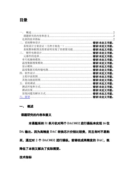
目录一、概述 (2)课题研究的内容和意义 (2)达到的技术指标 (2)二、系统整体设计................................................................................ 错误!未定义书签。
系统设计方案论证(几种方案选一).......................................... 错误!未定义书签。
系统整体框图及简要说明实现了的要紧功能.............................. 错误!未定义书签。
三、硬件电路设计.............................................................................. 错误!未定义书签。
元器件的选择.................................................................................. 错误!未定义书签。
单片机操纵模块................................................................................ 错误!未定义书签。
温度数据搜集模块............................................................................ 错误!未定义书签。
显示模块............................................................................................ 错误!未定义书签。
温度数据无线传输电路.................................................................... 错误!未定义书签。
Intel 16位单片机[87C196_MD]应用手册
Intel Corporation assumes no responsibility for the use of any circuitry other than circuitry embodied in an Intel product. No other circuit patent licenses are implied. Information contained herein supersedes previously published specifications on these devices from Intel.©INTEL CORPORATION, 2004 August 2004 Order Number:272543-0038XC196MH INDUSTRIAL MOTOR CONTROLCHMOS MICROCONTROLLERThe 8XC196MH is a member of Intel’s family of 16-bit MCS ® 96 microcontrollers. It is designed primarily to control three-phase AC induction and DC brushless motors. It features an enhanced three-phase waveform generator specifically designed for use in “inverter” motor-control applications. This peripheral provides pulse-width modulation and three-phase sine wave generation with minimal CPU intervention. It generates three complementary non-overlapping PWM pulses with resolutions of 0.125 µs (edge triggered) or 0.250 µs (centered).The 8XC196MH has two dedicated serial port peripherals, allowing less software overhead. The watchdog timer can be programmed with one of four time options.The 8XC196MH is available as the 80C196MH, which does not have on-chip ROM, the 87C196MH,which contains 32 Kbytes of on-chip OTPROM* or factory programmed ROM, and the 83C196MH, whichcontains 32 Kbytes of factory programmed MASK ROM. It is available in 84-lead PLCC, 80-lead Shrink EIAJ/QFP,and 64-lead SDIP. The 64-lead package does not contain pins for the P5.1/INST and P6.7/PWM1 signals.Operational characteristics are guaranteed over the temperature range of – 40°C to +85°C .*One-Time Programmable Read-Only Memory (OTPROM) is similar to EPROM but comes in an unwindowed package and cannot be erased. It is user programmable.■High Performance CHMOS 16-bit CPU ■16MHz Operating Frequency ■32Kbytes of On-chip OTPROM/ROM ■744Bytes of On-chip Register RAM ■Register-to-register Architecture ■16Prioritized Interrupt Sources■Peripheral Transaction Server (PTS)with 15Prioritized Sources ■Up to 52I/O Lines■3-phase Complementary Waveform Generator ■8-channel 8-or 10-bit A/D with Sample and Hold ■2-channel UART■Event Processor Array (EPA)with 2 High-speed Capture/Compare Modules and 4 High-speed Compare-only Modules ■Two Programmable 16-bit Timers with Quadrature Counting Inputs ■Two Pulse-width Modulator (PWM)Outputs with High Drive Capability ■Flexible 8- or 16-bit External Bus ■ 1.75µs 16× 16 Multiply ■3µs 32/16Divide■Extended Temperature Available ■Idle and Powerdown Modes ■Watchdog Timer8XC196MH INDUSTRIAL MOTOR CONTROL CHMOS MICROCONTROLLER2Figure 1. 8XC196MH Block Diagram8XC196MH INDUSTRIAL MOTOR CONTROL CHMOS MICROCONTROLLER3PROCESS INFORMATIONThis device is manufactured on PX29.5, a CHMOS IV process. Additional process and reliability information is available in Intel’s Components Quality and Reliability Handbook (order number 210997).All thermal impedance data is approximate for static air conditions at 1 watt of power dissipation. Values will change depending on operating conditions andthe application. The Intel Packaging Handbook (order number 240800) describes Intel’s thermal impedance test methodology.Table 1. Thermal Characteristics Package Type θJA θJC 84-lead PLCC 33°C/W 11°C/W 80-lead QFP 56°C/W 12°C/W 64-lead SDIP56°C/WN/AFigure 2. The 8XC196MH Family NomenclatureTo address the fact that many of the package prefix variables have changed, all package prefix variables in this document are now indicated with an "x".NOTE:8XC196MH INDUSTRIAL MOTOR CONTROL CHMOS MICROCONTROLLER4Table 2. 8XC196MH Memory MapAddress(1)Description Notes0FFFFH0A000HExternal Memory09FFFH02080HInternal ROM/OTPROM or External Memory0207FH0205EHReserved1, 2 0205DH02040HPTS Vectors0203FH02030HInterrupt Vectors (upper)0202FH02020HROM/OTPROM Security Key0201FH0201CHReserved1, 2 0201BH Reserved (must contain 20H)0201AH CCB102019H Reserved (must contain 20H)02018H CCB002017H02014HReserved02013H02000HInterrupt Vectors (lower)01FFFH01F00HInternal SFRs1 1EFFH300HExternal Memory2FFH18HRegister RAM3 17H00HCPU SFRs1 NOTES:1.Unless otherwise noted, write 0FFH to reserved memory locations and write 0 to reserved SFR bits.2.WARNING: The contents and/or function of reserved locations may change with future revisions of thedevice.3.Code executed in locations 0000H to 02FFH will be forced external.8XC196MH INDUSTRIAL MOTOR CONTROL CHMOS MICROCONTROLLER5Table 3. Signals Arranged by Functional CategoriesAddress & Data Programming Control Input/Output Input/Output (Cont’d)AD15:0AINC#P0.0/ACH0P2.5/COMP1CPVER P0.1/ACH1P2.6/COMP2Bus Control & Status PACT#P0.2/ACH2P2.7/SCLK1#/BCLK1ALE/ADV#PALE#P0.3/ACH3P3.7:0BHE#/WRH#PBUS15:0P0.4/ACH4P4.7:0BUSWIDTH PMODE.3:0P0.5/ACH5P5.7:0INST PROG#P0.6/ACH6/T1CLK P6.0/WG1#READY PVERP0.7/ACH7/T1DIR P6.1/WG1RD#P1.0/TXD0P6.2/WG2#WR#/WRL#Processor Control P1.1/RXD0P6.3/WG2EA#P1.2/TXD1P6.4/WG3#Power & Ground EXTINT P1.3/RXD1P6.5/WG3ANGND NMI P2.0/EPA0P6.6/PWM0V CC ONCE#P2.1/SCLK0#/BCLK0P6.7/PWM1V PP RESET#P2.2/EPA1V REF XTAL1P2.3/COMP3V SS XTAL2P2.4/COMP0NOTE:The following signals are not available in the 64-pin package: P5.1, P6.7, INST, and PWM1.8XC196MH INDUSTRIAL MOTOR CONTROL CHMOS MICROCONTROLLER6Figure 3. 8XC196MH 64-lead Shrink DIP (SDIP) Package8XC196MH INDUSTRIAL MOTOR CONTROL CHMOS MICROCONTROLLER 7Table 4. 64-lead Shrink DIP (SDIP) Pin AssignmentPin Name Pin Name Pin Name Pin Name 1V SS17P3.7/AD7/PBUS.733P6.2/WG2#49P0.0/ACH02P5.0/ALE/ADV#18P3.6/AD6/PBUS.634P6.1/WG150P2.0/EPA0/PVER 3V PP19P3.5/AD5/PBUS.535P6.0/WG1#51P2.1/SCLK0#/BCLK0/PALE#4P5.3/RD#20P3.4/AD4/PBUS.436P1.3/RXD152P2.2/EPA1/PROG#5P5.5/BHE#/WRH#21P3.3/AD3/PBUS.337P1.2/TXD153P2.3/COMP36P5.2/WR#/WRL#22P3.2/AD2/PBUS.238P1.1/RXD054P2.4/COMP0/AINC#7P5.7/BUSWIDTH 23P3.1/AD1/PBUS.139P1.0/TXD055P2.5/COMP1/PACT#8P4.6/AD14/PBUS.1424P3.0/AD0/PBUS.040P0.7/ACH7/T1DIR /PMODE.356P2.6/COMP2/CPVER 9P4.5/AD13/PBUS.1325RESET#41P0.6/ACH6/T1CLK/PMODE.257P2.7/SCLK1#/BCLK110P4.7/AD15/PBUS.1526NMI 42ANGND 58P6.6/PWM011V CC27EA#43V REF59XTAL212P4.4/AD12/PBUS.1228V SS 44P0.5/ACH5/PMODE.160XTAL113P4.3/AD11/PBUS.1129V CC45P0.4/ACH4/PMODE.061V SS14P4.2/AD10/PBUS.1030P6.5/WG346P0.3/ACH362 EXTINT 15P4.1/AD9/PBUS.9 31P6.4/WG3#47P0.2/ACH263P5.4/ONCE#16P4.0/AD8/PBUS.832P6.3/WG248P0.1/ACH164P5.6/READY8XC196MH INDUSTRIAL MOTOR CONTROL CHMOS MICROCONTROLLER8Figure 4. 8XC196MH 84-lead PLCC Package8XC196MH INDUSTRIAL MOTOR CONTROL CHMOS MICROCONTROLLER 9Table 5. 84-lead PLCC Pin AssignmentPin Name Pin Name Pin Name Pin Name 1P5.4/ONCE#22NC 43V SS64P2.0/EPA0/PVER 2P5.6/READY 23NC44P6.2/WG2#65P2.1/SCLK0#/BCLK0/PALE#3P5.1/INST 24P3.7/AD7/PBUS.745P6.1/WG166NC 4V SS25P3.6/AD6/PBUS.646P6.0/WG1#67NC 5P5.0/ALE/ADV#26P3.5/AD5/PBUS.547P1.3/RXD168P2.2/EPA1/PROG#6V PP27P3.4/AD4/PBUS.448P1.2/TXD169P2.3/COMP37P5.3/RD#28P3.3/AD3/PBUS.349NC 70P2.7/SCLK1#/BCLK18P5.5/BHE#/WRH#29P3.2/AD2/PBUS.250NC 71NC 9NC30P3.1/AD1/PBUS.151P1.1/RXD072NC10P5.2/WR#/WRL#31P3.0/AD0/PBUS.052P1.0/TXD073P2.4/COMP0/AINC#11P5.7/BUSWIDTH 32NC 53P0.7/ACH7/T1DIR/PMODE.374P2.5/COMP1/PACT#12P4.7/AD15/PBUS.1533RESET#54P0.6/ACH6/T1CLK/PMODE.275P2.6/COMP2/CPVER 13P4.6/AD14/PBUS.1434NMI 55ANGND 76P6.7/PWM114V CC35NC 56V REF77P6.6/PWM015P4.5/AD13/PBUS.1336EA#57P0.5/ACH5/PMODE.178NC 16NC 37V SS 58P0.4/ACH4/PMODE.079NC 17P4.4/AD12/PBUS.1238NC 59P0.3/ACH380NC 18P4.3/AD11/PBUS.1139V CC60P0.2/ACH281XTAL219P4.2/AD10/PBUS.1040P6.5/WG361P0.1/ACH182XTAL120P4.1/AD9/PBUS.941P6.4/WG3#62P0.0/ACH083V SS 21P4.0/AD8/PBUS.842P6.3/WG263NC84EXTINT8XC196MH INDUSTRIAL MOTOR CONTROL CHMOS MICROCONTROLLER10Figure 5. 8XC196MH 80-lead Shrink EIAJ/QFP PackageTable 6. 80-lead Shrink EIAJ/QFP Pin AssignmentPin Name Pin Name Pin Name Pin Name1P5.2/WR#/WRL#21NC41P0.7/ACH7/T1DIR/PMODE.361P2.4/COMP0/AINC#2P5.7/BUSWIDTH22RESET#42P0.6/ACH6/T1CLK/PMODE.262P2.5/COMP1/PACT#3P4.7/AD15/PBUS.1523NMI43ANGND63P2.6/COMP2/CPVER4P4.6/AD14/PBUS.1424EA#44VREF64P6.7/PWM15VCC 25VSS45P0.5/ACH5/PMODE.165P6.6/PWM06P4.5/AD13/PBUS.1326NC46P0.4/ACH4/PMODE.066NC7NC27VCC47P0.3/ACH367NC8P4.4/AD12/PBUS.1228P6.5/WG348P0.2/ACH268NC9P4.3/AD11/PBUS.1129P6.4/WG3#49P0.1/ACH169XTAL210P4.2/AD10/PBUS.1030P6.3/WG250P0.0/ACH070XTAL111P4.1/AD9/PBUS.931VSS 51NC71VSS12P4.0/AD8/PBUS.832P6.2/WG2#52P2.0/EPA0/PVER72EXTINT13P3.7/AD7/PBUS.733P6.1/WG153P2.1/SCLK0#/BCLK0/PALE#73P5.4/ONCE# 14P3.6/AD6/PBUS.634P6.0/WG1#54NC74P5.6/READY 15P3.5/AD5/PBUS.535P1.3/RXD155NC75P5.1/INST16P3.4/AD4/PBUS.436P1.2/TXD156P2.2/EPA1/PROG#76VSS17P3.3/AD3/PBUS.337NC57P2.3/COMP377P5.0/ALE/ADV#18P3.2/AD2/PBUS.238NC58P2.7/SCLK1#/BCLK178VPP19P3.1/AD1/PBUS.139P1.1/RXD059NC79P5.3/RD#20P3.0/AD0/PBUS.040P1.0/TXD060NC80P5.5/BHE#/WRH#PIN DESCRIPTIONSTable 7. Signal DescriptionsSignal Name Type DescriptionMultiplexedWithACH7 ACH6 ACH5 ACH4 ACH3:0I Analog Channels. These pins are analog inputs to the A/Dconverter.These pins are multiplexed with the port 0 pins. While it ispossible for the pins to function simultaneously as analog anddigital inputs, this is not recommended because reading theport while a conversion is in process can produce unreliableconversion results.The ANGND and VREFpins must be connected for the A/Dconverter and the multiplexed port pins to function.P0.7/T1DIR/PMODE.3P0.6/T1CLK/PMODE.2P0.5/PMODE.1P0.4/PMODE.0P0.3:0AD15:8 AD7:0I/O Address/Data Lines. These pins provide a multiplexedaddress and data bus. During the address phase of the buscycle, address bits 0–15 are presented on the bus and canbe latched using ALE or ADV#. During the data phase, 8- or16-bit data is transferred.P4.7:0/PBUS.15:8P3.7:0/PBUS.7:0ADV#O Address Valid. This active-low output signal is asserted onlyduring external memory accesses.ADV# indicates that valid address information is available onthe system address/data bus. The signal remains low while avalid bus cycle is in progress and is returned high as soon asthe bus cycle completes.An external latch can use the ADV# signal to demultiplex theaddress from the address/data bus. Used with a decoder,ADV# can generate chip-selects for external memory.P5.0/ALEAINC#I Auto Increment. In slave programming mode, this active-lowinput signal enables the autoincrement mode. Auto incrementallows reading from or writing to sequential OTPROMlocations without requiring address transactions across theprogramming bus for each read or write.P2.4/COMP0ALE O Address Latch Enable. This active-high output signal isasserted only during external memory cycles.ALE signals the start of an external bus cycle and indicatesthat valid address information is available on the systemaddress/data bus. ALE differs from ADV# in that it is notreturned high until a new bus cycle is to begin.An external latch can use ALE to demultiplex the addressfrom the address/data bus.P5.0/ADV#ANGND GND Analog Ground. Reference ground for the A/D converterand the logic used to read port 0. ANGND must be held atnominally the same potential as VSS .—BCLK1 BCLK0I Serial Communications Baud Clock 0 and 1. BCLK0 and 1are alternate clock sources for the serial ports. The maximuminput frequency is FOSC/4.P2.7/SCLK1#P2.1/SCLK0#/PALE#BHE#O Byte High Enable. During 16-bit bus cycles, this active-lowoutput signal is asserted for word reads and writes and forhigh-byte reads and writes to external memory. BHE#indicates that valid data is being transferred over the upperhalf of the system address/data bus.BHE#, in conjunction with A0, selects the memory byte to beaccessed:BHE#A0Byte(s) Accessed00both bytes01high byte only10low byte onlyP5.5/WRH#BUSWIDTH I Bus Width. When enabled in the chip configuration register,this active-high input signal dynamically selects the bus widthof the bus cycle in progress. When BUSWIDTH is high, a 16-bit bus cycle occurs; when BUSWIDTH is low, an 8-bit buscycle occurs. BUSWIDTH is active during a CCR fetch.P5.7COMP3 COMP2 COMP1 COMP0O Event Processor Array (EPA) Compare Pins. Thesesignals are the output of the EPA compare modules. Thesepins are multiplexed with other signals and may beconfigured as standard I/O.P2.3P2.6/CPVERP2.5/PACT#P2.4/AINC#CPVER O Cumulative Program Verification. This active-high outputsignal indicates whether any verify errors have occurredsince the device entered programming mode. CPVERremains high until a verify error occurs, at which time it isdriven low. Once an error occurs, CPVER remains low untilthe device exits programming mode. When high, CPVERindicates that all locations have programmed correctly sincethe device entered programming mode.P2.6/COMP2EA#I External Access. This active-low input signal directsmemory accesses to on-chip or off-chip memory. If EA# islow, the memory access is off-chip. If EA# is high and thememory address is within 2000H–2FFFH, the access is toon-chip ROM or OTPROM. Otherwise, an access with EA#high is to off-chip memory.EA# is sampled only on the rising edge of RESET#.If EA# = VEA on the rising edge of RESET#, the device entersthe programming mode selected by PMODE.3:0.For devices without ROM, EA# must be tied low.—EPA1 EPA0I/O Event Processor Array (EPA) Input/Output pins. Theseare the high-speed input/output pins for the EPAcapture/compare modules. These pins are multiplexed withother signals and may be configured as standard I/O.P2.2/PROG#P2.0/PVER Table 7. Signal Descriptions (Continued)Signal Name Type DescriptionMultiplexedWithEXTINT I External Interrupt. This programmable interrupt is controlledby the WG_PROTECT register. This register controlswhether the interrupt is edge triggered or sampled andwhether a rising edge/high level or falling edge/low levelactivates the interrupt. This interrupt vectors through memorylocation 203CH. If the chip is in idle mode and if EXTINT isenabled, a valid EXTINT interrupt brings the chip back tonormal operation, where the first action is to execute theEXTINT service routine. After completion of the serviceroutine, execution resumes at the instruction following theone that put the chip into idle mode.In powerdown mode, a valid EXTINT interrupt causes thechip to return to normal operating mode. If EXTINT isenabled, the EXTINT service routine is executed. Otherwise,execution continues at the instruction following the IDLPDinstruction that put the chip into powerdown mode.—INST O Instruction Fetch. This active-high output signal is valid onlyduring external memory bus cycles. When high, INSTindicates that an instruction is being fetched from externalmemory. The signal remains high during the entire bus cycleof an external instruction fetch. INST is low for dataaccesses, including interrupt vector fetches and chip configu-ration byte reads. INST is low during internal memoryfetches.P5.1NMI I Nonmaskable Interrupt. In normal operating mode, a risingedge on NMI causes a vector through the NMI interrupt atlocation 203EH. NMI must be asserted for greater than onestate time to guarantee that it is recognized.In idle mode, a rising edge on NMI brings the chip back tonormal operation, where the first action is to execute the NMIservice routine. After completion of the service routine,execution resumes at the instruction following the one thatput the chip into idle mode.In powerdown mode, NMI causes a return to normaloperating mode only if it is tied to EXTINT.—ONCE#I On-circuit Emulation. Holding this pin low while theRESET# signal transitions from a low to a high places thedevice into on-circuit emulation (ONCE) mode. ONCE modeisolates the device from other components in the system toallow the use of a clip-on emulator for system debugging.This mode puts all pins except XTAL1 and XTAL2 into a high-impedance state. To exit ONCE mode, reset the device bypulling the RESET# signal low. P5.4Table 7. Signal Descriptions (Continued)Signal Name Type DescriptionMultiplexedWithP0.7 P0.6 P0.5 P0.4 P0.3:0I Port 0. This is a high-impedance, input-only port. Port 0 pinsshould not be left floating.These pins may individually be used as analog inputs(ACH x) or digital inputs (P0.x). While it is possible for the pinsto function simultaneously as analog and digital inputs, this isnot recommended because reading port 0 while a conversionis in process can produce unreliable conversion results.ANGND and VREFmust be connected for port 0 and the A/Dconverter to function.ACH7/T1DIR/PMODE.3ACH6/T1CLK/PMODE.2ACH5/PMODE.1ACH4/PMODE.0ACH3:0P1.3 P1.2 P1.1 P1.0I Port 1. This is a 4-bit, bidirectional, standard I/O port that ismultiplexed with individually selectable special-functionsignals. (Used as PBUS.15:12 in Auto-programming Mode.)RXD1TXD1RXD0TXD0P2.7 P2.6 P2.5 P2.4 P2.3 P2.2 P2.1 P2.0I/O Port 2. This is an 8-bit, bidirectional, standard I/O port that ismultiplexed with individually selectable special-functionsignals. P2.6 is multiplexed with a special test mode function.To prevent accidental entry into test modes, always configureP2.6 as an output.SCLK1#/BCLK1COMP2/CPVERCOMP1/PACT#COMP0/AINC#COMP3EPA1/PROG#SCLK0#/BCLK0/PALE#EPA0/PVERP3.7:0I/O Port 3. This is an 8-bit, bidirectional, memory-mapped I/Oport with open-drain outputs. The pins are shared with themultiplexed address/data bus, which has complementarydrivers.In programming modes, port 3 serves as the low byte of theprogramming bus (PBUS).AD7:0/PBUS.7:0P4.7:0I/O Port 4. This is an 8-bit, bidirectional, memory-mapped I/Oport with open-drain outputs. The pins are shared with themultiplexed address/data bus, which has complementarydrivers.In programming modes, port 4 serves as the high byte of theprogramming bus (PBUS).AD15:8/PBUS.15:8P5.7 P5.6 P5.5 P5.4 P5.3 P5.2 P5.1 P5.0I/O Port 5. This is an 8-bit, bidirectional, standard I/O port that ismultiplexed with individually selectable control signals.Because P5.4 is multiplexed with the ONCE# function,always configure it as an output to prevent accidental entryinto ONCE mode.BUSWIDTHREADYBHE#/WRH#ONCE#RD#WR#/WRL#INSTALE/ADV# Table 7. Signal Descriptions (Continued)Signal Name Type DescriptionMultiplexedWithP6.7 P6.6 P6.5 P6.4 P6.3 P6.2 P6.1 P6.0O Port 6. This is an 8-bit output port that is multiplexed with the special functions of the waveform generator and PWMperipherals. The WG_OUT register configures the pins,establishes the output polarity, and controls whether changesto the outputs are synchronized with an event or take effectimmediately.PWM1PWM0WG3WG3#WG2WG2#WG1WG1#PACT#O Programming Active. In auto-programming mode, PACT#low indicates that programming activity is occurring.P2.5/COMP1PALE#I Programming ALE. In slave programming mode, this active-low input indicates that ports 3 and 4 contain acommand/address. When PALE# is asserted, data andcommands on ports 3 and 4 are read into the device.P2.1/SCLK0#/BCLK0PBUS.15:8 PBUS.7:0I/O Programming Bus. In programming modes, used as abidirectional port with open-drain outputs to pass commands,addresses, and data to or from the device. Used as a regularsystem bus to access external memory during auto-programming mode. When using slave programming mode,the PBUS is used in open-drain I/O port mode (not as asystem bus). In slave programming mode, you must addexternal pull-up resistors to read data from the device duringthe dump word routine.P4.7:0/AD15:8P3.7:0/AD7:0PMODE.3 PMODE.2 PMODE.1 PMODE.0I Programming Mode Select. Determines the OTPROMprogramming algorithm that is to be performed. PMODE issampled after a device reset when EA# = VEAand must bestable while the device is operating.P0.7/ACH7/T1DIRP0.6/ACH6/T1CLKP0.5/ACH5P0.4/ACH4PROG#I Programming Start. This active-low input is valid only inslave programming mode. The rising edge of PROG# latchesdata on the PBUS and begins programming. The falling edgeof PROG# ends programming.P2.2/EPA1PVER O Program Verification. In programming modes, this active-high output signal is asserted to indicate that the word hasprogrammed correctly. (PVER low after the rising edge ofPROG# indicates an error.)P2.0/EPA0PWM1:0O Pulse Width Modulator Outputs. These are PWM outputpins with high-current drive capability. The duty cycle andfrequency-pulse-widths are programmable.P6.7:6RD#O Read. Read-signal output to external memory. RD# isasserted only during external memory reads.P5.3Table 7. Signal Descriptions (Continued)Signal Name Type DescriptionMultiplexedWithREADY I Ready Input. This active-high input signal is used tolengthen external memory cycles for slow memory bygenerating wait states.When READY is high, CPU operation continues in a normalmanner. If READY is low, the memory controller inserts waitstates until the READY signal goes high or until the numberof wait states is equal to the number programmed into thechip configuration register.READY is ignored for all internal memory accesses.P5.6RESET#I/O Reset. Reset input to and open-drain output from the chip. Afalling edge on RESET# initiates the reset process. WhenRESET# is first asserted, the chip turns on a pull-downtransistor connected to the RESET pin for 16 state times.This function can also be activated by execution of the RSTinstruction. In the powerdown and idle modes, assertingRESET# causes the chip to reset and return to normaloperating mode. RESET# is a level-sensitive input.—RXD1 RXD0I/O Receive Serial Data 0 and 1. In modes 1, 2, and 3, RXD0 and 1 are used to receive serial port data. In mode 0, theyfunction as either inputs or open-drain outputs for data.P1.3P1.1SCLK1# SCLK0#I/O Synchronous Clock Pin 0 and 1. In mode 4, these are thebidrectional, shift clock signals that synchronize the serialdata transfer. Data is transferred 8 bits at a time with the LSBfirst. The DIR bit (SP_CON x.7) controls the direction ofSCLK x signal.DIR = 0The internal shift clock is output on SCLK x.DIR = 1An external shift clock is input on SCLK x.P2.7/BCLK1P2.1/BCLK0T1CLK I External Clock. External clock for timer 1. Timer 1increments (or decrements) on both rising and falling edgesof T1CLK. Also used in conjunction with T1DIR forquadrature counting mode.P0.6/ACH6/PMODE.2T1DIR I Timer 1 External Direction. External direction (up/down) fortimer 1. Timer 1 increments when T1DIR is high anddecrements when it is low. Also used in conjunction withT1CLK for quadrature counting mode.P0.7/ACH7/PMODE.3TXD1 TXD0O Transmit Serial Data 0 and 1. In serial I/O modes 1, 2, and 3, TXD0 and 1 are used to transmit serial port data. In mode0, they are used as the serial clock output.P1.2P1.0V CC PWR Digital Supply Voltage. Connect each VCCpin to the digital supply voltage.—V PP PWR Programming Voltage. Set to 12.5 V when programming the on-chip OTPROM. Also the timing pin for the “return frompower-down” circuit.—Table 7. Signal Descriptions (Continued)Signal Name Type DescriptionMultiplexedWithV REF PWR Reference Voltage for the A/D Converter. VREFis also the supply voltage to the analog portion of the A/D converter andthe logic used to read Port 0. VREFmust be connected for the A/D and port 0 to function.—V SS GND Digital Circuit Ground (0 volts). Connect each VSSpin to ground.—WG3 WG2 WG1O Waveform Generator Phase 1–3 Positive Outputs.3-phase output signals used in motion-control applications.P6.5P6.3P6.1WG3# WG2# WG1#O Waveform Generator Phase 1–3 Negative Outputs.Complementary 3-phase output signals used in motion-control applications.P6.4P6.2P6.0WR#O Write. This active-low output indicates that an external writeis occurring. This signal is asserted only during externalmemory writes.P5.2/WRL#WRH#O Write High. During 16-bit bus cycles, this active-low outputsignal is asserted for high-byte writes and word writes toexternal memory.During 8-bit bus cycles, WRH# is asserted for all writeoperations.P5.5/BHE#WRL#O Write Low. During 16-bit bus cycles, this active-low outputsignal is asserted for low-byte writes and word writes.During 8-bit bus cycles, WRL# is asserted for all writeoperations.P5.2/WR#XTAL1I Clock/Oscillator Input. Input to the on-chip oscillatorinverter and the internal clock generator. Also provides theclock input for the serial I/O baud-rate generator, timers, andPWM unit. If an external oscillator is used, connect theexternal clock input signal to XTAL1 and ensure that theXTAL1 VIH specification is met.—XTAL2O Oscillator Output. Output of the on-chip oscillator inverter.When using the on-chip oscillator, connect XTAL2 to anexternal crystal or resonator. When using an external clocksource, let XTAL2 float.—Table 7. Signal Descriptions (Continued)Signal Name Type DescriptionMultiplexedWithELECTRICAL CHARACTERISTICSABSOLUTE MAXIMUM RATINGS*Storage Temperature ................................ – 65°C to + 150°C Ambient Temperatureunder Bias.............................................. – 40°C to + 85°C Voltage from V PP or EA# toV SS or ANGND (Note 1)...................... – 0.5 V to + 13.0 V Voltage with respect toV SS or ANGND (Note 1)........................ – 0.5 V to + 7.0 V (This includes V PP on ROM and CPU devices.)Power Dissipation.......................................................... 1.5 W(based on package heat transfer limitations, not device power consumption)OPERATING CONDITIONS*T A (Ambient Temperature Under Bias).........– 40°C to + 85°C V CC (Digital Supply Voltage) .......................... 4.50 V to 5.50 V V REF (Analog Supply Voltage) ....................... 4.50 V to 5.50 V F OSC (Oscillator Frequency) (Note 2)........... 8 MHz to 16 MHzNOTES:1.ANGND and V SS should be at nominally the samepotential.2.Testing is performed down to 8 MHz, althoughthe device is static by design and will typically operate below 1 Hz.NOTICE : This data sheet contains preliminary infor-mation on new products in production. It is valid forthe devices indicated in the revision history. The specifications are subject to change without notice.*WARNING : Stressing the device beyond the “Absolute Maximum Ratings” may cause permanent damage. These are stress ratings only. Operation beyond the “Operating Conditions” is not recommended and extended exposure beyond the “Operating Conditions” may affect device reli-ability.。
Infineon(英飞凌)单片机教案PPT
CAN接口电路
CAN接口芯片
CAN总线
“Controller Area Network”,即控制器局 域网,是国际上应用最广泛的现场总线之 一。 一个由CAN 总线构成的单一网络中,理论 上可以挂接无数个节点 实际上同一网络中最多可挂接110个节点 通常电压值为:CAN_H = 3.5V 和CAN_L = 1.5V 。
XC167CI实验板功能模块介绍
XC167-CI实验板
XC167CI简装开发板的特点
英飞凌系列的XC167CI采用的是TQFP144 的封装形式 板上的双重电源可以为XC167CI提供5V伏 / 2点6伏的电压。 高速的CAN收发器,LIN 收发器,EPROM, URAT(RS232串口) 8位低功耗的LED
数据存储区地址映射
程序存储区
XC167中有两个片上程序存储区,用于代码/数据存储 256KB程序FLASH/ROM,C0’0000H…C3’FFFFH存 储代码和常量数据。FLASH可以通过软件(反复) 编程,ROM只能在工厂掩模编程 6KB程序SRAM(PSRAM)E0’0000H…E0’17FFH 存储临时代码和其它数据,比如高级引导加载程序 可写在PRAM中,继而执行该程序对片上存储器进 行编程
微型计算机的组成框图 (由多个IC芯片组装在一个主电路板上)
所有单元都组装 在一个IC芯片上
Infineon单片机分类
根据每种型号的存储器的类型分类
无ROM型:C167CR-LM ROM型 :C167CR-16RM OTP型 :C164CI-8EM FLASH型 :XC167CI-32F
第二部分:XC167CI实验板简介
最新纯中文版英飞凌DAP miniWiggler的使用开发宝典
最新纯中文版英飞凌DAP miniWiggler的使用开发宝典单片机开发除了必要程序编写外同样也离不开下载器与仿真器。
miniWiggler是目前英飞凌单片机最流行的仿真器。
英飞凌miniwiggler使用步骤1、安装最新版本的DAS,从供应商或从以下链接下载(\miniwiggler)2、把miniwiggler连接到电脑上的任意一个USB接口。
电脑会自动适别这个新设备并自动安装相庆的驱动程序。
3、把下载线连接到目标板上4、启动您的调试工具选择DAS的服务器udas或以上的USB芯片的JTAG。
DAS的服务器的使用1、启动调试工具选择DAS2、3、4、最后出现XC166-Family表示安装成功Keil C166与miniwiggler的使用工程的详细设置首先点击Project窗口中的Target1 Project->Option for Target1 “Debug”即出现对工程设置的对话框.选择”Infineon DAS Client for XC166”选择片内的FLASH.仿真与下载以上即完成了工程的相关设置,接下来可以进行编译,连接。
选择菜单ProjectBuild target或单击图标对当前工程进行连接。
编译过程中的信息将出现在输出窗口中的Build页,如果源程序中有语法错误,会有错误报告出现,单击该行会有相应的错误报告出现。
编译成功后提示获得*.hex文件,该文件可被编译器读入并写入芯片中,同时还产生了一些其他相关文件可用于Keil的仿真与调试。
在对工程成功编译,连接后,按F5或点击菜单Debug Start/StopDebug Session或单击图即可进入调试状态。
DAP miniWiggler经济划算的高性能调试工具miniWiggler是英飞凌面向未来的经济划算的高性能调试工具。
在主机侧,它具备一个USB接口。
每台计算机都具备USB接口。
在器件侧,则可通过英飞凌10-针DAP或16-针OCDSL1接口,进行通信。
英飞凌单片机例程tc1767_taskingv33r2_dcm_ltc
Create by Dave
Main.c Main.h Gpta0.c Gpta0.h Io.c Io.h
confidential
Page 28
Exercise GPTA_LTC_DCM Tasking Viper : Setting Target Board
Create Project name „GPTA_LTC_DCM ´ Select ‘Use default location’ Select ‘Empty project’ Click ‘Next’
Same name as DAvE directory
1
confidential
Page 26
Exercise GPTA_LTC_DCM Tasking Viper:Create New Project(cont.)
Page 27
Exercise GPTA_LTC_DCM Tasking Viper : Reflash Project
Refresh files in the project Right click on „GPTA_LTC_DCM‟ in the navigator
Select „Refresh‟ from the pull down menu
confidential
Page 22
Exercise GPTA_LTC_DCM Tasking Viper : Open a workspace
Start TASKING VX-toolset for tricore Click on Open Project Work Space Filename: browse to “d:\hot\tc1767” Click „OK‟