ZigBee JN5148模块介绍
基于ZigBee的无线传感网设计

基于ZigBee的无线传感网设计□刘靓贵州大学职业技术学院贵州电子信息职业技术学院【摘要】基于ZigBee的无线传感网具有低价、低传输率、短距离、低功率的特点,在工业监控、农业、医疗卫生、智能家居等领域有广阔的应用前景,本文分析了基于ZigBee的无线传感网系统设计及传感器节点设计,对实际工程具有重要的指导意义。
【关键词】ZigBee无线传感网传感器CC24301无线传感网应用及Zig-Bee技术无线传感网是由部署在监测区域内大量的廉价微型传感器节点组成,通过无线通信方式形成的一个多跳的自组织的网络系统,其目的是协作感知、采集和处理网络覆盖区域中感知对象的信息,并发送给观察者,是一种新型的无线通讯网络。
它综合了传感器技术、嵌入式处理技术、无线通信及网络技术、分布式处理技术等多领域、多学科研究成果,其具有类型众多的传感器,可探测包括温度、湿度、噪声、亮度、压力、物体移动速度和方向等各种各样的物理现象,在工业监控、农业、医疗卫生、智能家居等领域都有着广阔的应用前景。
Zigbee是目前应用最为广泛的新技术ew Technology N56无线传感网络协议,是由Zigbee 联盟在IEEE802.15.4标准上定义了网络层、安全层及应用层等,于2004年12月正式获得批准,具有低功耗、低成本、大容量、短时延、协议简单和安全性高等优点,无线传感网采用Zigbee技术具有良好的通用性和可扩展性。
IEEE802.15.4标准中有关物理层部分规定了两个工作频段,分别位于2.4GHz、868/915MHz频段。
其中2.4GHz频段为全球统一的无需申请的ISM频段,有助于ZigBee设备推广和降低生产成本。
2.4GHz频段物理层采用直接序列扩频技术的(DSSS)O-QPSK 调制方式能提供最高250kb/s的传输速率,能够满足一般传感器节点的通信需求。
2基于ZigBee的无线传感网系统设计无线传感网系统结构采用ZigBee协议树状结构,包括传感器节点、无线传感网网关和计算机。
ZigBee1085 无线数据采集卡 说明书

4
版本:6.020
北京阿尔泰科技发展有限公司
功能码
1 BYTE
0x02
字节计数
1 BYTE
N
输入状态
n BYTE
n =N or N+1
N =读取数量/8 如果余数不为 0 则 N=N+1
错误 响应
功能码
1 BYTE
0x02+ 0x80
错误代码
1 BYTE
0x1 or 0x2
举例
请求
响应
模块地址
数据(hex)
00
字节计数
03
起始地址低(字节)
00
00(h)~07 状态
CD
读取数量高(字节)
00
读取数量低(字节)
08
2)、读开关量输入
功能码:02 数据起始地址:10001~10016 说明:读取输入开关量的状态
数据说明: 地址
10001 10002 10003 10004 保留 MODBUS 请求 功能码 起始地址 读取数量 MODBUS 响应
1
ZigBee1085 无线数据采集卡硬件使用说明书
GND.R: 数字量输入地端 2. LED 指示灯
ZIGBEE1082 模块有 2 个指示灯,分别为 c 黄灯: 网络指示灯,ZIGBEE1082 模块加入网络后,此灯闪烁 d 红灯: 通讯指示灯,ZIGBEE1082 模块与数据中心通讯时,此灯闪烁 3. 网络复位键 点击此键可复位本机的 ZIGBEE 网络,使模块重新搜寻网络 4. RS232 接口 对 XBEE 模块进行配置时,使用此口与计算机连接
0xA3(12 时制)
Bit15~Bit8: 无效, 写 0
40516
hac-embee-a11n 2.4g 低功耗无线数传模块(zigbee)用户手册说明书
HAC-EmBee-A11D HAC-EmBee-A11N2.4G低功耗无线数传模块(ZigBee)用户手册V 2.02.2 2013/10/25深圳市华奥通通信技术有限公司SHENZHEN HAC TELECOM TECHNOLOGY CO.,LTD地址 : 深圳市南山区西丽路4227号大学城创意园2栋6楼电话 : +86-755-23981078传真 : +86-755-23981007邮件:*****************************网址 : HAC EmBee ZigBee Series 深圳市华奥通通信技术有限公司高性能✧20dbm可视距离2.8km✧7dbm可视距离850m 低功耗✧20dbm发射电流145mA,接收电流38mA,休眠电流3uA✧7dbm发射电流42mA,接收电流29mA,休眠电流3uAMESH网络✧自动组网,自动路由,自动愈合✧点对点,点对多点传输✧最多高达16跳传输 使用简单✧AT命令✧API命令✧API远程AT命令✧透明传输符合标准✧Zigbee 2007 Pro✧A11 Profile高可靠性✧DSSS O-QPSK调制方式✧CSMA-CA 自动退避机制✧重发与应答机制高安全性✧网络层AES加密✧应用层AES加密目录1 EmBee模块 (6)1.1 EmBee模块尺寸及管脚顺序 (6)1.2 模块管脚分布 (7)1.3 模块性能参数 (8)1.3.1 HAC-EmBee-A11N参数 (8)1.3.2 HAC-EmBee-A11D参数 (9)2 EmBee模块操作 (10)2.1 UART串口介绍 (10)2.2 通信协议 (10)2.2.1 透明传输模式 (10)2.2.2 API传输模式 (11)2.3 AT命令模式 (11)2.3.1 进入AT命令模式 (12)2.3.2 发送AT命令 (12)2.3.3 AT命令响应 (12)2.3.4 退出AT命令模式 (13)2.4 回环功能 (13)2.4.1 透传模式的回环 (13)2.4.2 API模式的回环 (13)3 API操作 (14)3.1 API帧格式 (14)3.2 API帧 (15)3.2.1 AT命令帧(立即生效) (15)3.2.2 AT命令帧(不立即生效) (16)3.2.3 AT命令响应帧 (17)3.2.4 传输请求帧 (18)3.2.5 应用层可选的传输请求帧 (19)3.2.6 传输状态帧 (21)3.2.1 数据接收指示帧(AO=0) (22)3.2.2 数据接收指示帧(AO=1) (23)3.2.3 I/O接收指示 (24)3.2.4 节点发现指示 (26)3.2.5 模块状态指示帧 (28)3.2.6 远端AT命令请求帧 (29)3.2.7 远端AT命令响应帧 (30)4 AT命令 (32)4.1 地址命令 (32)4.2 网络命令 (34)4.3 射频参数命令 (36)4.4 串口参数命令 (37)4.5 I/O参数命令 (38)4.6 诊断参数命令 (41)4.7 AT命令参数 (42)4.8 休眠命令 (42)4.9 命令执行 (43)5 数字I/O和模拟I/O (45)5.1 本地I/O (45)5.1.1 AT命令模式下读取本地I/O电平值和采样值 (45)5.1.1 AT命令模式下配置本地I/O (46)5.1.2 API模式下配置本地I/O (47)5.2 远端I/O (47)5.2.1 API模式下配置远端I/O (47)6 EmBee ZigBee网络 (48)6.1 协调器 (48)6.2 路由器 (49)6.3 终端设备 (49)6.3.1 子节点与父节点关系 (50)6.3.2 子节点容量 (50)6.4 子节点工作过程 (51)6.5 父节点工作过程 (51)1EmBee模块1.1EmBee模块尺寸及管脚顺序EmBee模块的外形结构如下:管脚顺序从PIN1开始,逆时针依次至PIN20。
zigbee技术资料整理
Zigbee技术资料搜集整理一、Zigbee技术1、简介在蓝牙技术的使用过程中,人们发现蓝牙技术尽管有许多优点,但仍存在许多缺陷。
对工业,家庭自动化控制和遥测遥控领域而言,蓝牙技术显得太复杂,功耗大,距离近,组网规模太小等,……而工业自动化对无线通信的需求越来越强烈。
正因此,经过人们长期努力,Zigbee协议在2003年中通过后,于2004正式问世了。
ZigBee技术是一种应用于短距离范围内,低传输数据速率下的各种电子设备之间的无线通信技术。
ZigBee名字来源于蜂群使用的赖以生存和发展的通信方式,蜜蜂通过跳ZigZag形状的舞蹈来通知发现的新食物源的位置、距离和方向等信息,以此作为新一代无线通讯技术的名称。
ZigBee过去又称为“HomeRF Lite”、“RF-EasyLink”或“FireFly”无线电技术,目前统一称为Zigbee技术。
2、ZigBee是什么ZigBee是一个由可多到65000个无线数传模块组成的一个无线数传网络平台,十分类似现有的移动通信的CDMA网或GSM网,每一个ZigBee网络数传模块类似移动网络的一个基站,在整个网络范围内,它们之间可以进行相互通信;每个网络节点间的距离可以从标准的75米,到扩展后的几百米,甚至几公里;另外整个ZigBee网络还可以与现有的其它的各种网络连接。
例如,你可以通过互联网在北京监控云南某地的一个ZigBee控制网络。
不同的是,ZigBee网络主要是为自动化控制数据传输而建立,而移动通信网主要是为语音通信而建立;每个移动基站价值一般都在百万元人民币以上,而每个ZigBee"基站"却不到1000元人民币;每个ZigBee 网络节点不仅本身可以与监控对对象,例如传感器连接直接进行数据采集和监控,它还可以自动中转别的网络节点传过来的数据资料;除此之外,每一个ZigBee网络节点(FFD)还可在自己信号覆盖的范围内,和多个不承担网络信息中转任务的孤立的子节点(RFD)无线连接。
ZigBee无线传感器网络教学实验平台开发

ZigBee无线传感器网络教学实验平台开发作者:石建国马云辉张华斌师向群来源:《物联网技术》2013年第06期摘要:针对实践教学和创新训练需要,设计了基于ZigBee的无线传感器网络实验平台和教学方案,详细阐述了ZigBee无线传感器网络实验平台的硬件结构、软件开发方法和教学实施过程。
该平台中的三类节点设备均以JN5148无线微控制器为核心,硬件采用模块化结构。
实践表明,利用该平台开展多层次、案例化教学和项目设计训练,可使学生较快掌握ZigBee 无线传感器网络的相关技术要点,有效提高无线传感器网络的应用开发能力。
关键词:ZigBee;ZigBee PRO;无线传感器网络;WSN;JN5148;实验平台中图分类号:TP393;G642.423 文献标识码:A 文章编号:2095-1302(2013)06-0028-030 引言无线传感器网络(Wireless Sensor Network,WSN)是由大量微型智能传感器节点以无线多跳方式形成的自组织网络,在军事、工业、农业、医疗、交通、环境监测、智能家居等诸多领域有着广阔的应用前景[1-2]。
近几年,随着物联网概念的兴起,特别是我国高校开设物联网专业以来,作为物联网重要支撑技术的WSN进一步成为研究、应用的热点[3-6]。
ZigBee是建立在IEEE802.15.4协议规范基础之上的新兴无线网络技术,与Bluetooth、Wi-Fi等相关技术相比,ZigBee更适合低速WSN中对成本、安全性、动态组网和功耗有特殊要求的节点之间的无线互连[7-8]。
ZigBee增强版ZigBee PRO于2007年发布,已有多家知名半导体厂商为其提供芯片、协议栈和开发环境支持。
针对电子科技大学中山学院学生实践教学和创新训练需要,设计了一套基于ZigBee的WSN实验平台。
平台中传感器终端、路由器、协调器三类节点设备均以JN5148无线微控制器为核心,硬件采用模块化结构。
19_无线RS485模块使用说明书

QZ01-485/232无线模块使用说明书重庆勤智科技有限公司使用本公司模块前,请仔细阅读本说明书。
一、概述ZigBee是一种用于控制和监视各种系统的低数据速率低功耗联网无线标准。
ZigBee 所依据的IEEE 802.15.4 标准规定了ZigBee的数据传输速率应在20 kbps、40 kbps 或250 kbps,并且采用ZigBee 的设备应能至少工作两年而无需更换电池。
ZigBee 拟应用于环境控制系统、安全系统、工业传感器以及医疗监控系统等传输数据量少、负载周期短的系统。
本说明书涉及到的QZ01-485-100和QZ01-485-1600均采用飞思卡尔半导体(原摩托罗拉半导体)的经济高效的单封装(SiP)MC13213 ZigBee解决方案。
运用ZigBee技术的家庭消费类产品包括:带有照明和HVAC控制设备的家庭自动化系统、安全系统、百叶窗控制及遥控器、以及用于机顶盒和其他娱乐设备的远程控制。
带有附件接口的消费产品可在售后增加ZigBee功能,例如掌上电脑或笔记本电脑中的紧凑型闪存或PCMCIA插槽。
本说明书包括两种模块:QZ01-485-100和QZ01-485-1600模块。
QZ01-485-100模块采用IEEE802.15.4标准和ZigBee协议,采用单片集成电路,通信距离不小于100m;QZ01-485-1600模块是增强型的ZigBee模块,具有通信距离远、抗干扰能力强、组网灵活等优点和特性;可实现一点对多点及多点对多点之间的设备间数据的透明传输;可组成星型和网状网络结构。
二、性能指标●设备省电ZigBee技术采用了多种节电的工作模式,可以确保两节五号电池工作长达6个月到两年。
●通信可靠ZigBee采用了CSMA/CA的碰撞避免机制,同时为需要固定带宽的通信业务预留了专用时隙,避免了发送数据的竞争和冲突;MAC层采用了完全确认的数据传输机制,每个发送的数据包都必须等待接收方的确认信息。
青鸟JBF5145输入输出模块使用说明书
故障状态:“输入动作”灯不亮,“输出动作”灯不亮
二线制(无极性) 1~200
专用电子编码器 1500m
第2页,共5页
兼容性
JBF5145 型输入/输出模块使用说明书V1.0
1.1 产品特点
● 内置微处理器; ● 采用 SMT 表面贴装工艺; ● 具有一组最大能量 DC27V/1.5A/300ms 输出端口; ● 模块工作电压范围广,可在 DC18-28V 范围内正常工作; ● 通信采用二总线技术,无极性要求; ● 施工中建议使用双绞线,导线截面积不小于1.5mm²; ● 回路信号处理电路与输入输出检测信号处理电路实现电气隔离,模块稳定性高,抗干扰能力强; ● 电子编码方式,可通过专用电子编码器编址; ● 模块采用易于客户施工、维护的插拔式结构。先安装底座,线路检查完成后再装主体进行开通调试。 ● 具备完善的故障检测功能(包括输入、输出端的断路、短路检测)。
向上
安装
④
④
VO+
VO- S- 5
em[ 10%
eml[ 10%
1N4007
及馈 EQU
4.2 调试方法
图 3 接线示意图
● 首先使用电子编码器对JBF5145 输入/输出模块进行编码。
● 模块安装好后操作控制器对其进行登记,然后必须在系统中手动将其设置成电池储能设备。
● 进入手动启停现场设备界面,输入要启动的模块回路及地址启动,模块输出动作指示灯变为红 色常亮,被控设备动作,模块收到被控设备的无源反馈后输入动作指示灯变为红色常亮。
JN5121-xxx-Myy IEEE802.15.4 ZigBee模块系列初步数据手册说明书
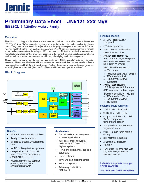
Preliminary Data Sheet – JN5121-xxx-MyyIEEE802.15.4/ZigBee Module FamilyPreliminary - JN-DS-JN5121-xxx-Myy v1.1 © Jennic 2006OverviewThe JN5121-xxx-Myy is a family of surface mounted modules that enable users to implement IEEE802.15.4 or ZigBee compliant systems with minimum time to market and at the lowest cost. They remove the need for expensive and lengthy development of custom RF board designs and test suites. The modules use Jennic’s JN5121 wireless microcontroller to provide a comprehensive solution, including all RF components. All that is required to develop and manufacture wireless control or sensing products is to connect a power supply and peripherals such as switches, actuators, sensors, considerably simplifying product development.Three basic hardware module variants are available: JN5121-xxx-M00 with an integrated antenna, JN5121-xxx-M01/M03 with an antenna connector and JN5121-xxx-M02/M04 with a power amplifier and LNA for extended range. Each of these can be provided pre-programmed with a ZigBee network stack (JN5121-Z01-Myy) or with customer-specific software.Block DiagramJennicii Preliminary - JN-DS-JN5121-xxx-Myy v1.1 © Jennic 2006Contents1. Introduction11.1.Variants12. Specifications 23. Product Development33.1. JN5121 Single Chip Wireless Microcontroller 34. Pin Configurations 44.1. Pin Assignment 5 4.2. Pin Descriptions 6 4.3. Power Supplies6 4.4.SPI Memory Connections6 5. Electrical Characteristics75.1. Maximum Ratings 7 5.2. Operating Conditions7 Appendix A Mechanical and Ordering Information 8 A.1 Outline Drawing8 A.2 Module PCB Footprint 11 A.3 Ordering Information 12 A.4 Accessories13 A.5 Tape and Reel Information:14 A.5.1 Tape Orientation and dimensions 14 A.5.2 Cover tape details 14 A.5.3 Leader and Trailer 15 A.5.4 Reel Dimensions: 15 A.6 Related Documents 16 A.7 Disclaimers 17 A.8 Version Control 17 A.9 Contact Details18Jennic Jennic© Jennic 2006 Preliminary - JN-DS-JN5121-xxx-Myy v1.1 11. IntroductionThe JN5121-xxx-Myy module family provides designers with a ready made component which allows IEEE802.15.4 [1]wireless applications, including ZigBee, to be quickly and easily included in product designs. The modules integrate all of the RF components, removing the need to perform expensive RF design and test. Products can be designed by simply connecting sensors and switches to the module IO pins. The modules use Jennic’s single chip IEEE802.15.4 Wireless Microcontroller, allowing designers to make use of the extensive chip development support material. Hence, this range of modules allows designers to bring wireless applications to market in the minimum time with significantly reduced development effort and cost.Three basic modules are available: JN5121-xxx-M00 (standard module with on board ceramic antenna), JN5121-xxx-M01 (standard module with SMA connector for use with external antennae) and JN5121-xxx-M02 (high RF power, improved sensitivity module for extended range applications). Each of these modules can be supplied with a range of protocol stacks, including a simple IEEE802.15.4 protocol for point to point and star applications and a ZigBee mesh networking stack. The variants available are described below.1.1. VariantsVariantDescriptionJN5121-000-M00 JN5121 Module (IEEE802.15.4 stack, ceramic antenna) JN5121-Z01-M00 JN5121 Module (ZigBee stack, ceramic antenna) JN5121-000-M01 JN5121 Module (IEEE802.15.4 stack, SMA connector) JN5121-Z01-M01 JN5121 Module (ZigBee stack, SMA connector)JN5121-000-M02 JN5121 Module (High Power (18.5dBm), IEEE802.15.4 stack, SMA connector) JN5121-Z01-M02 JN5121 Module (High Power (18.5dBm), ZigBee stack, SMA connector) JN5121-000-M03 JN5121 Module (IEEE802.15.4 stack, RP-SMA connector) JN5121-Z01-M03 JN5121 Module (ZigBee stack, RP-SMA connector)JN5121-000-M04 JN5121 Module (High Power (18.5dBm), IEEE802.15.4 stack, RP-SMA connector) JN5121-Z01-M04JN5121 Module (High Power (18.5dBm), ZigBee stack, RP-SMA connector)Jennic2 Preliminary - JN-DS-JN5121-xxx-Myy v1.1 © Jennic 20062. SpecificationsMost specification parameters for the modules are specified in JN-DS-JN5121 Datasheet for JN5121 single chip wireless microcontroller, [2]. Where there are differences, the parameters are defined here. VDD=3.0V @ +25ºCTyp. DC CharacteristicsNotesJN5121-xxx-M00/01/03 JN5121-xxx- M02/04 Deep sleep <11uA <11uASleep <14uA <14uA With active sleep timer Radio transmit 44mA 115mA CPU in doze, radio transmitting Radio receive49mA 60mA CPU in doze, radio receiving Centre frequency accuracy+/-25ppm+/-25ppmAdditional +/-15ppm allowance for temperature and agingTyp. RF CharacteristicsNotesReceive sensitivity -90dBm -93dBm Nominal for 1% PER, as per 802.15.4 section 6.5.3.3 Max. Transmit power 0dBm 16dBm Nominal Transmit power at 3.6V 18.5dBm With Vcc=3.6VMaximum input signal -10dBm-15dBm For 1% PER, measured as sensitivity RSSI range-95 to -10 dBm -115 to -20 dBmRF Port impedance - SMA connector 50 ohm 50 ohm 2.4 - 2.5GHz VSWR (max)2:12:12.4 - 2.5GHzPeripheralsNotesMaster SPI port with five select outputs 250kHz - 16MHz Slave SPI port 250kHz - 16MHz Two UARTs16550 compatible Two-wire serial I/F (compatible with SMbus & I 2C) Up to 400kHz Two programmable Timer/Counters with capture/compare facility, Tick timer 16MHz clock Two programmable Sleep Timers32kHz clock Twenty-one digital IO lines (multiplexed with UARTs, timers and SPI selects)Four-channel, 12-bit, Analogue-to-Digital converterUp to 100ks/s Two 11-bit Digital-to-Analogue converters Up to 100ks/sProgrammable analogue comparatorUltra low power mode for sleepInternal temperature sensor and battery monitorJennic Jennic© Jennic 2006 Preliminary - JN-DS-JN5121-xxx-Myy v1.1 33. Product DevelopmentJennic supplies all the development tools and networking stacks needed to enable end product development to occurquickly and efficiently. These are all freely available from Jennic’s support website: /support/ . A range of evaluation/developer kits is also available, allowing products to be quickly breadboarded. Efficient development of software applications is enabled by the provision of a complete, unlimited, software developer kit. Together with the available libraries for the IEEE802.15.4 MAC and the ZigBee network stack, this package provides everything required to develop application code and to trial it with hardware representative of the final module. The modules can be programmed by the user, for both development and production, using Jennic supplied software. They can also be supplied ready loaded with customer defined software if required. The JN-UG-3007 Flash Loader User Guide [5], describes how to put the module into programming mode, download software onto the module and to load individual MAC addresses. Access to the on-chip peripherals, MAC and ZigBee stack software is provided through specific APIs. These are described in the JN-RM-2001 Hardware Peripheral Library Reference Manual [3], JN-RM-2002 Stack Software Reference Manual [4] and JN-RM-2014 ZigBee Application Development API Reference Manual [6]. Additional information is available on the Jennic support website.3.1. JN5121 Single Chip Wireless MicrocontrollerThe JN5121-xxx-Myy series is constructed around the JN5121 single chip wireless microcontroller, which includes the radio system, a 32-bit RISC CPU, ROM and RAM memory and a range of analogue and digital peripherals. The chip is described fully in JN-DS-JN5121 Datasheet for JN5121 single chip wireless microcontroller [2].Jennic4 Preliminary - JN-DS-JN5121-xxx-Myy v1.1 © Jennic 2006ADC4DAC1DAC2COMP+COMP-SPICLK SPIMISO SPIMOSI SPISSZDIO0/SPISEL1DIO1/SPISEL2DIO2/SPISEL3SPISSM SPISWP DIO3/SPISEL4D I O 4/C T S 0D I O 5/R T S 0D I O 6/T X D 0D I O 7/R X D 0D I O 8/T I M 0G T D I O 9/T I M 0_C A PD I O 10/T I M 0_O U T D I O 11/T I M 1G TV D D G N D V S S AADC3ADC2ADC1NC NCDIO20/RXD1DIO19/TXD1DIO18/RTS1DIO17/CTS1DIO16DIO15/SIF_D RESETNDIO14/SIF_CLK DIO13/TIM1_OUT DIO12/TIM1_CAPFigure 1: Pin Configuration (top view)Note that the same basic pin configuration applies for all module designs. However, DIO3/SPISEL4 and DIO2/SPISEL3 are not available with high power modules.Jennic Jennic© Jennic 2006 Preliminary - JN-DS-JN5121-xxx-Myy v1.1 54.1. Pin AssignmentModulePin SignalFunctionAlternative Function1 ADC4 Analogue to Digital input2 DAC1 Digital to Analogue output3 DAC2 Digital to Analogue output4 COMP+5 COMP- Comparator inputs6 SPICLK SPI master clock out/slave clock in7 SPIMISO SPI Master In/Slave Out8 SPIMOSI SPI Master Out/Slave In9 SPISSZ SPI select from module - SS0 (output)10 SPISEL1 SPI Slave Select1 (output) General Purpose Digital I/O DIO0 11 SPISEL2 SPI Slave Select2 (output) General Purpose Digital I/O DIO1 12 SPISEL3* SPI Slave Select3 (output) General Purpose Digital I/O DIO2 * 13 SPISSM SPI select to FLASH (input)14 SPISWP FLASH write protect (input) 15 SPISEL4* (not on Hi SPI Slave Select4 (output) General Purpose Digital I/O DIO3* 16 CTS0 UART0 Clear To Send (input) General Purpose Digital I/O DIO4 17 RTS0 UART0 Request To Send (output) General Purpose Digital I/O DIO5 18 TXD0 UART0 Transmit Data (output) General Purpose Digital I/O DIO6 19 RXD0 UART0 Receive Data (input) General Purpose Digital I/O DIO7 20 TIM0GT Timer0 clock/gate (input) General Purpose Digital I/O DIO8 21 TIM0_CAP Timer0 capture (input) General Purpose Digital I/O DIO9 22 TIM0_OUT Timer0 PWM (output) General Purpose Digital I/O DIO10 23 TIM1GT Timer1 clock/gate (input) General Purpose Digital I/O DIO11 24 VDD 3V power 25 GND Digital ground 26 VSSA Analogue ground 27 TIM1_CAP Timer1 capture (input) General Purpose Digital I/O DIO12 28 TIM1_OUT Timer1 PWM (output) General Purpose Digital I/O DIO13 29 RESETN Active low reset30SIF_CLKSerial Interface clock / Intelligent peripheral clockGeneral Purpose Digital I/O DIO14Jennic6 Preliminary - JN-DS-JN5121-xxx-Myy v1.1 © Jennic 2006ModulePin SignalFunctionAlternative Function31 SIF_D Serial Interface data / Intelligent peripheral data outGeneral Purpose Digital I/O DIO15 32 DIO 16 Intelligent peripheral device select General Purpose Digital I/O 33 CTS1 UART1 Clear To Send (input) General Purpose Digital I/O DIO17 34 RTS1 UART1 Request To Send (output) General Purpose Digital I/O DIO18 35 TXD1 UART1 Transmit Data (output) General Purpose Digital I/O DIO19 36 RXD1 UART1 Receive Data (input) General Purpose Digital I/O DIO2037 NC 38 NC Connect to ground39 ADC1 Analogue to Digital input 40 ADC2 Analogue to Digital input 41ADC3Analogue to Digital input *: These two pins are not connected for High power modules4.2. Pin DescriptionsAll pins behave as described in the JN5121 datasheet [2], with the exception of the following:4.3. Power SuppliesA single power supply pin, VDD is provided. Separate analogue (VSSA) and digital (GND) grounds are provided. These should be connected together at the module pins.4.4. SPI Memory ConnectionsSPISWP is a write protect pin for the serial flash memory. This should be held low to inhibit writes to the flash device. SPISSZ is connected to SPI Slave Select 0 on the JN5121. SPISSM is connected to the Slave Select pin on the memory.This configuration allows the flash memory device to be programmed using an external programmer if required. The JN5121 should be held in reset by taking RESETN low. The memory can then be programmed over the UART by using the programming mode described in JN-UG-3007 Flash Loader User Guide [5]. Alternatively, the memory can be programmed by connecting a SPI programmer to SPISSM, SPICLK, and SPIMISO and directly loading the code into the memory.For normal operation of the module, SPISSZ should be connected to SPISSM.Jennic Jennic© Jennic 2006 Preliminary - JN-DS-JN5121-xxx-Myy v1.1 75. Electrical CharacteristicsIn most cases, the Electrical Characteristics are the same for both module and chip. They are described in detail inthe chip datasheet. Where there are differences, they are detailed below.5.1. Maximum RatingsExceeding these conditions will result in damage to the device.ParameterMin Max Device supply voltage VDD1, VDD2 -0.3V3.6VVoltage on analogue pins ADC1-4, DAC1-2, COMP2M, COMP2P-0.3V VDD + 0.3VVoltage on 5V tolerant digital pins SPICLK,SPIMOSI, SPIMISO, SPISEL0, GPIO0-GPIO20, RESETN-0.3VVDD + 2V or 5.5V, whichever is the lesserStorage temperature-40ºC 150ºC Solder reflow temperature (According to IPC/JEDEC J-STD-020C)260 °CThis device is sensitive to ESD and should only be handled using ESD precautions.5.2. Operating ConditionsSupplyMin Max VDD2.7V3.6V Ambient temperature range-20ºC70ºCJennic8 Preliminary - JN-DS-JN5121-xxx-Myy v1.1 © Jennic 2006Appendix A Mechanical and Ordering InformationA.1 Outline Drawingmm2.54mmmm1.27mmThickness: 3mmJN5121-xxx-M00 Outline Drawing2.79 mm 2.54 mm2.54 mm 1.27 mmThickness: 3mm over can, 10.6mm at SMA connectorJN5121-xxx-M01/M03 Outline Drawingmm 1.27 mmmmThickness: 3mm, 10.6mm at SMA connectorJN5121-xxx-M02/M04 Outline DrawingA.2 Module PCB FootprintAll Pads are 0.9mm square on 1.27mm pitch1.27mmNote: All modules have the same footprint.A.3 Ordering InformationPart Numbering:Software Variant000 IEEE802.15.4 Stack Z01 ZigBee StackShippingR Box (10 modules per pack) T Tape Mounted 500pcs (00 module only) V Tape Mounted 200pcs (01,02,03,04 modulesonly)Temp Range / Device Status D -20°C to +70°C, QualifiedModule Type 00 Standard Power, Ceramic antenna 01 Standard Power, SMA connector 02 High Power, SMA connector 03 Standard Power, RP-SMA connector 04 High power, RP-SMA connectorA.4 AccessoriesProduct DescriptionNoteJNAC001 JN5 serial level converter dongleConnects module UART port to PC serial port to allow code development and debugThe JNAC001 RS-232 level converter is used to translate the +/- 7V RS-232 levels to CMOS compatible logic levels.The CMOS levels are made available through a short flying lead with a 6-way IDC socket. This can be connected to the relevant module UART0 pins. The RS-232 Interface is available on a standard nine-way ‘D’ connector.J1C T R R TD SFigure 5-1: JNAC001 RS-232 Converter Connection26View looking at cableconnectorFigure 5-2: RS-232 ConnectorA.5 Tape and Reel Information:A.5.1 Tape Orientation and dimensionsModule type: A B W F E P0 P1 P2 T Cover Tapewidth (W) JN5121-xxx-M00 18.4 30.4 44 20.2 1.75 4.0 2.0 24.0 3.2 37.5JN5121-xxx-M01/3 18.4 30.4 56 20.2 1.75 4.0 2.0 24.0 11.4 49.5JN5121-xxx-M02/4 18.4 40.5 56 20.2 1.75 4.0 2.0 24.0 11.4 49.5 Tolerance ±0.1 ±0.1 ±0.3 ±0.1 +0.1 ±0.1 ±0.1 ±0.1 ±0.1A.5.2 Cover tape detailsThickness (T) 0.061mmSurface resistivity (component side) 104 to 107 Ohms/sqSurface resistivity (component side) Non-conductiveBacking type: PolyesterAdhesive type: PSASealing: Room ambientA.5.3 Leader and TrailerA.5.4 Reel Dimensions:Module type: A B C N W (min)JN5121-xxx-M00 330 ±1.0 2.2±0.5 13 ±0.2 100 +0.1 44.5 ±0.3JN5121-xxx-330 ±1.0 2.2±0.5 13 ±0.2 100 +0.1 56.5 ±0.3 M01/02/03/04A.6 Related Documents[1] IEEE Std 802.15.4-2003 IEEE Standard for Information Technology – Part 15.4 Wireless Medium Access Control(MAC) and Physical Layer (PHY) Specifications for Low-Rate Wireless Personal Area Networks (LR-WPANs)[2] JN-DS-JN5121 Datasheet for JN5121 single chip wireless microcontroller[3] JN-RM-2001 Hardware Peripheral Library Reference Manual[4] JN-RM-2002 Stack Software Reference Manual[5] JN-UG-3007 Flash Loader User Guide[6] JN-RM-2014 ZigBee Application Development API Reference ManualRoHS ComplianceJN5121-xxx-Myy devices meet the requirements of Directive 2002/95/EC of the European Parliament and of the Council on the Restriction of Hazardous Substance (RoHS).Status InformationThe status of this Data Sheet is Preliminary.Jennic products progress according to the following format:AdvanceThe Data Sheet shows the specification of a product in planning or in development.The functionality and electrical performance specifications are target values and may be used as a guide to the final specification.Jennic reserves the right to make changes to the product specification at anytime without notice.PreliminaryThe Data Sheet shows the specification of a product that is in production, but is not yet fully qualified.The functionality of the product is final. The electrical performance specifications are target values and may used as a guide to the final specification. Modules are identified with an R suffix, for example JN5121-Z01-M00R.Jennic reserves the right to make changes to the product specification at anytime without notice.ProductionThis is the final Data Sheet for the product.All functional and electrical performance specifications, including minimum and maximum values are final.This Data Sheet supersedes all previous document versions.Jennic reserves the right to make changes to the product specification at anytime to improve its performance.A.7 DisclaimersThe contents of this document are subject to change without notice. Jennic reserves the right to make changes, without notice, in the products, including circuits and/or software, described or contained herein in order to improve design and/or performance. Information contained in this document regarding device applications and the like is intended through suggestion only and may be superseded by updates. It is your responsibility to ensure that your application meets with your specifications.Jennic assumes no responsibility or liability for the use of any of these products, conveys no license or title under any patent, copyright, or mask work right to these products, and makes no representations or warranties that these products are free from patent, copyright, or mask work infringement, unless otherwise specified.Jennic products are not intended for use in life support systems, appliances or systems where malfunction of these products can reasonably be expected to result in personal injury, death or severe property or environmental damage. Jennic customers using or selling these products for use in such applications do so at their own risk and agree to fully indemnify Jennic for any damages resulting from such use.All trademarks are the property of their respective owners.A.8 Version ControlVersion Notes0.9 1st Issue of Preliminary Datasheet1.0 Update performance parameters & Ordering / Tape & Reel informationA.9 Contact Details Corporate HeadquartersJennic Ltd, Furnival StreetSheffield S1 4QT, UKTel: +44 (0)114 281 2655Fax: +44 (0) 114 281 2951***************Jennic Ltd JapanOsakaya building 4F1-11-8 Higashigotanda Shinagawa-ku Tokyo 141-0022, JapanTel: +81 3 5449 7501Fax: +81 3 5449 0741**************.comJennic Ltd Taiwan19F-1, 182, Sec.2 Tun Hwa S. Road. Taipei 106, TaiwanTel: +886 2 2735 7357Fax: +886 2 2739 5687**************.comJennic America Inc - East Coast Office 1322 Scott Street, Suite 203Point Loma, CA 92106, USATel: +619 223 2215Fax: +619 223 2081**************.comJennic America Inc - West Coast Office 1060 First Avenue, Suite 400King of Prussia, PA 19406, USATel: +1 484 868 0222Fax: +1 484 971 5015**************.com。