2015 m0601 l04 curve modeling x2
XSAV11373型号的OsiSense XS系列产品数据手册说明书
D i s c l a im e r: T h i s d o c u m e n t a t i o n i s n o t i n t e n d e d a s a s u b s t i t u t e f o r a n d i s n o t t o b e u s e d f o r d e t e r m i n i n g s u i t a b i l i t y o r r e l i a b i l i t y o f t h e s e p r o d u c t s f o r s p e c i f i c u s e r a p p l i c a t i o n sProduct data sheetCharacteristicsXSAV11373inductive sensor XSAV - M30 - Sn10mm -6..150c/mn - 12..48VDC - cable 2mProduct availability : Stock - Normally stocked in distribution facilityPrice* : 168.64 USDMainRange of product OsiSense XS Series name ApplicationSensor type Inductive proximity sensor Device application Rotation monitoring Sensor name XSASensor design Cylindrical M30Size 81 mm Body typeFixedDetector flush mounting acceptance Flush mountable MaterialMetalEnclosure material Nickel plated brass Type of output signal Discrete Wiring technique3-wire[Sn] nominal sensing distance 0.39 in (10 mm)Discrete output function 1 NC Output circuit type DC Discrete output type PNP Electrical connection Cable Cable length6.56 ft (2 m)[Us] rated supply voltage 12...48 V DC with reverse polarity protection Switching capacity in mA <= 200 mA with overload and short-circuit protection IP degree of protectionIP67 conforming to IEC 60529ComplementaryThread type M30 x 1.5Detection faceFrontalFront material PPSAdjustable frequency range 6...150 cyc/mnOperating zone0...0.31 in (0...8 mm)Differential travel 3...15% of FrRepeat accuracy3% of SrCable composition 3 x 0.34 mm²Wire insulation material PvRStatus LED 1 LED red output stateSupply voltage limits10...58 V DCSwitching frequency<= 100 HzVoltage drop<= 1.8 V at closed stateCurrent consumption0...15 mAat no-loadRun-up delay at power-up9 s standardMarking CEThreaded length 2.24 in (57 mm)Height 1.18 in (30 mm)Length 3.19 in (81 mm)Product weight0.66 lb(US) (0.3 kg)EnvironmentProduct certifications CCCCSAULAmbient air temperature for operation-13...158 °F (-25...70 °C)Ordering and shipping detailsCategory22486 - SENSORS, PROXIMITYDiscount Schedule DS2GTIN00785901231813Nbr. of units in pkg.1Package weight(Lbs)0.53000000000000003Returnability YCountry of origin FROffer SustainabilitySustainable offer status Green Premium productRoHS (date code: YYWW)Compliant - since 0825 - Schneider Electric declaration of conformitySchneider Electric declaration of conformityREACh Reference not containing SVHC above the thresholdReference not containing SVHC above the thresholdProduct environmental profile AvailableProduct end of life instructions AvailableCalifornia proposition 65WARNING: This product can expose you to chemicals including:- - - - - - - Substance 1Diisononyl phthalate (DINP), which is known to the State of California to cause cancer, and- - - - - - - Substance 2Di-isodecyl phthalate (DIDP), which is known to the State of California to cause birth defects or otherreproductive harm.- - - - - - - More information For more information go to Contractual warrantyWarranty period18 monthsDimensions DrawingsDimensions(1)LEDMounting and ClearanceMinimum Mounting Distances Side by sidee (1) ≥20 mm/0.79 inFace to facee (2) ≥120 mm/4.72 inFacing a metal objecte (3) ≥30 mm/1.18 in.Connections and SchemaWiring Schemes3-wire DCBU :BlueBN :BrownBK :BlackPerformance CurvesPerformance CurvesStandard Steel Target : 30x30x1 mm(1)Pick-up points(2)Drop-out points (object approaching from the side)(y)Sensing distance in mm。
螺旋桨三维建模方法研究

摘要 : 推导了螺旋桨叶切面处局部坐标系到全局坐标系的坐标变换公式 , 并提出了相应的坐标点计算程序设计方法 , 在此基础上用实例介绍了在 Pro / ENGINEER绘图环境下的螺旋桨三维实体建模过程 。
关键词 : 螺旋桨 ; 坐标变换 ; 三维建模 中图分类号 : TP391172 文献标识码 : A 文章编号 : 1001 - 3881 (2006) 5 - 060 - 3
下的 Through Points选 项 , 然
后由底至顶逐点选取所生成
曲线族的端点 。至此完 成 了
螺旋桨空间边界曲线图 , 如
图 3 所示 , 面向我们观察方
向的为叶面方向 。
(5) 利用边界曲线图生 成螺旋桨桨叶曲面图 。边 界
(Boundaries) 是 曲 面 绘 制 经 常用到的方法 , 使用边界命
模型 。
最终生成的螺旋桨实体模型如图 4所示 。 4 结论
本文推导了螺旋桨叶切面局部坐标系到全局坐标 系的坐标转换公式 。从而解决了将图谱提供的空间叶 切面的几何数据应用到三维 CAD 造型过程之中的问 题 , 使整个造型过程变得简便直观 , 因此具有一定的 普遍意义 。
对于螺旋桨曲面创建过程 , 基于本文提出的方 法 , 可以简便地完成造型过程 , 可操作性强 。据此 , 对于常用的叶型 , 利用二次开发工具可以编制灵活而 实用的螺旋桨参数化设计制图软件 , 进而生成系列化 的螺旋桨 , 极大地提高了效率 。
Begin curve ! 2
1 11. 178253 166. 646916 40. 834568
2 15. 222363 166. 326269 40. 122382
奥克斯科普OX5042英文快速引导说明书

OscilloscopeModel OX 5042Quick Start GuideENGLISH(1) U.S. Wall Plug 18W, 100-240V, 50/60Hz Cat. #5000.51USB DRIVE CONTENTS: The SX-METRO software and the Handscope’s complete userAlso Included:(1) Test Report(1) Battery Information Sheet(6) 1.2V NiMH rechargeable batteries 2700mA/h Handscope OscilloscopeModel OX5042(2) Probe 10:1 600V/BNC-MCat. #5000.50PRODUCT PACKAGING 2150.21Shipping Contents:(1) Black Tool BagCat. #2133.72(1) USB Drive(software and manual)(1) Set of two,color-coded leads and clipsCat. #2140.63(1) BNC AdapterCat. #2118.46(1) USB Cable + DriverCat. #2135.41(1) Set of two, color-coded probes Cat. #2152.23(1) U.S. Wall Plug 18W, 100-240V , 50/60Hz Cat. #5000.51USB DRIVE CONTENTS: The SX-METRO software and the Handscope’s complete user Also Included:(1) Test Report(1) Battery Information Sheet(6) 1.2V NiMH rechargeable batteries 2700mA/h(1) Current Probe MN251TCat. #2132.59(1) USB Drive (software and manual)(1) Set of two,color-coded leads and clipsCat. #2140.63(1) BNC AdapterCat. #2118.46(1) Probe 10:1 600V/BNC-M Cat. #5000.50(1) USB Cable + DriverCat. #2135.41Shipping Contents:(1) Set of two, color-coded probes Cat. #2152.23(1) Current Probe MF3000-24-1-1Cat. #2132.63(1) Carrying CaseCat. #2155.77Handscope OscilloscopeModel OX5042(1) U.S. Wall Plug 18W, 100-240V , 50/60Hz Cat. #5000.51USB DRIVE CONTENTS: The SX-METRO software and the Handscope’s complete user Also Included:(1) Test Report(1) Battery Information Sheet(6) 1.2V NiMH rechargeable batteries 2700mA/h(1) Current Probe MN379TCat. #2153.02(1) USB Drive (software and manual)(1) Set of two,color-coded leads and clipsCat. #2140.63(1) BNC AdapterCat. #2118.46(1) Probe 10:1 600V/BNC-M Cat. #5000.50(1) USB Cable + DriverCat. #2135.41Shipping Contents:(1) Set of two, color-coded probes Cat. #2152.23(1) Current Probe MF3000-24-1-1Cat. #2132.63(1) Carrying CaseCat. #2155.77Handscope OscilloscopeModel OX5042Precautions Before UseThe operator and/or the responsible authority must carefully read and completely understand the precautions before use. If you use this instrument in an unspecified manner, the protection it ensures can be compromised, thus putting you in danger.• This instrument is designed for use:-indoors-in a level 2 pollution environment-at an altitude below 2000 m-at a temperature between 0° C and 40° C-with a relative humidity of less than 80% up to 35° C.• The safety of all systems, including the instrument, is the responsibility of the operator.• It can be used for measurements on 600V CAT III circuits, relative to the ground/ earth.• Before each use, check the condition of the insulation on the cables, boxes, sensors and accessories. Any element on which the insulation is damaged(even partially) must be taken out of service for repair or disposal.• Respect the environmental and storage conditions.• The external power supply must be connected to the instrument and to the network (98 to 264 V AC).• The power supply to the instrument is fitted with an automatically resettable electrical protection after disappearance of the fault.• As a safety measure, only use factory supplied parts and accessories.• It is advised to use individual safety protection whenever the environmental situations in which the instrument is used require it.• When handling the sensors or test probes, do not place your fingers beyond the physical guard.• If the battery housing cover is absent, damaged or incorrectly positioned, the instrument must not be used other than to adjust the sensors.Definition of Measurement Categories (CAT)CAT IV Measurement category IV corresponds to measurements taken at the source of low-voltage installations.Example: power feeders, counters and protection devices.CAT III Measurement category III corresponds to measurements on building installa-tions.Example: distribution panel, circuit-breakers, machines or fixed industrialdevices.CAT II Measurement category II corresponds to measurements taken on circuits directly connected to low-voltage installations.Example: power supply to domestic electrical appliances and portable tools.Symbols UsedCAUTION! Risk of electric shock. The voltage at theparts marked with this symbol may be dangerous.Warning: Risk of danger. Refer to the operating manual to find out the nature ofthe potential hazards and the action necessary to avoid such hazards.Earth/GroundDual insulationThe trash can with a line through it means that in the European Union, the prod-uct must undergo selective disposal for the recycling of electric and electronicmaterial, in compliance with Directive WEEE 2002/96/EC.The CE marking guarantees conformity with European directives and with regu-lations covering EMC.Application or withdrawal not authorized for non-insulated conductors carryingdangerous voltage levelsPower SupplyThe oscilloscope is supplied with one external power supply and set of 6 x 1.2V NiMH rechargeable batteries 2700mA/h.When the supplied wall plug is connected from the instrument to an external power source, battery power is not needed. The batteries are only used when there is no external power supply available.Before the first use, start by fully charging the battery.When the batteries are recharging, the Battery Charge LED on the front panel will turn on steady.The LED will blink in the following situations:• pre-charge of very low batteries• temperature is too low or too high• batteries are damagedWhen the charge is complete, the LED will turn off.If the batteries need to be replaced, they must be replaced with NiMH rechargeable batteries. Battery charge life is guaranteed for same-capacity batteries (in mAh) as those shipped with the oscilloscope.To remove the battery cover, use a coin to turn the slot on the back of the unit counter-clockwise.DescriptionThe Handscope Oscilloscope Model OX5042-CK combines three instruments into one:• 40MHz oscilloscope• Independent 8000-count multimeter with power measurements• Built-in harmonic analyzer out to the 31st harmonic (fundamental between 40 and 450Hz)The instrument operates at a constant acquisition depth of 2500 points.An LCD TF T screen is used to view the applied signals along with all the setting parameters.The main command functions are accessible using the buttons on the front panel.A graphic interface is used to:-adjust the parameters related to the selected button-navigate using a horizontal main menu showing the current settings andvertical sub-menusChannel IsolationThe two oscilloscope input channels are isolated from each other and from the ground/ earth and the main power supply block. This isolation is provided by double or rein-forced insulation, in compliance with the safety standards IEC 61010-1 and IEC 61010-2-030.This makes it possible to make measurements on installations or systems connected to the electricity supply network for voltages of up to 600V in CAT III. The common mode authorized between the two channels is 600V in CAT III. Thus the operator, the test systems and the environment are completely protected at all times.Any voltage (even dangerous) on one channel will not be present on the other channel. The low points of the inputs are completely insulated, so there is no possibility of the low points looping (which can be dangerous and highly destructive).The oscilloscope is rated 600V CAT III; at least 600V CAT III accessories must be used.Control FeaturesMeasurement Terminals12345109876InputChannel “A”InputChannel “B”External powersupplyUse of the 10:1 ProbesDistribution of stray capacitors:Considering the stray capacitances, it is imperative to correctly connect the reference conductors for each probe The conductors should preferably be connected to the cold points to avoid the transmission of noise by the stray capacitance between modes.The noise of the digital ground (earth) is sent to the analog input by the stray capaci-tance.10:1 Probe CalibrationTo obtain optimum response, the probe’s low frequency compensation must be adjusted.NOTE: T o carry out this adjustment, the two channels of your oscilloscope must be disconnected from the measured circuits before opening the battery housing cover.The calibration output (3Vpp, 1kHz) for the probe is underneath the battery cover.To remove the battery cover, use a coin to turn the slot on the back of the unit counter-clockwise.Connect the probe to be adjustedto the calibration output under thebattery housing cover, as shown.• Select the DC coupling for the channel to which the probe is connected and run an Autosetto carry out pre-setting. • Adjust the sensitivity and the vertical offset of the channel so that the signal fills the screen, and adjust the time base to 200µs to view a signal period on the screen.•Turn the BNC base of the probe in order to access the probe adjustment screw:In this example, the probe is over-compesated:an overshoot occurs.Turn the screw in either direction until thesignal is horizontal and looks like the screenshown opposite. Your probe is now calibrated.Turn the BNC base again to close access tothe adjustment screw and replace the batterycover.Remote ProgrammingThe oscilloscope can be programmed remotely from a computer by using the SX-METRO software, which is located on the CD-ROM supplied with your instrument. This software is used to:• Configure the instrument• Perform measurements and retrieve the results• Transfer files (traces, configuration, screenshots, etc.)To communicate between the instrument and the computer:• Connect the USB end of the cable to one of the PC’s USB ports (if necessary install the driver shipped with the cable).• Connect the optical connector to the oscilloscope, after first powering it up.• Open SX-METRO; select USB communications and wait for communication to be established (in the event of a problem, refer to the SX-METRO instructions).Repair and CalibrationTo ensure that your instrument meets factory specifications, we recommend that it be scheduled back to our factory Service Center at one-year intervals for recalibration, or as required by other standards or internal procedures.For instrument repair and calibration:You must contact our Service Center for a Customer Service Authorization Number (CSA#). This will ensure that when your instrument arrives, it will be tracked and pro-cessed promptly. Please write the CSA# on the outside of the shipping container. If the instrument is returned for calibration, we need to know if you want a standard calibra-tion, or a calibration traceable to N.I.S.T. (Includes calibration certificate plus recorded calibration data).Ship To: Chauvin Arnoux®, Inc. d.b.a. AEMC® Instruments15 Faraday DriveDover, NH 03820 USAPhone: (800) 945-2362 (Ext. 360)(603) 749-6434 (Ext. 360)Fax: (603) 742-2346 or (603) 749-6309E-mail:***************(Or contact your authorized distributor)Costs for repair, standard calibration, and calibration traceable to N.I.S.T. are available.NOTE: You must obtain a CSA# before returning any instrument.Technical and Sales AssistanceIf you are experiencing any technical problems, or require any assistance with the proper operation or application of your instrument, please call, mail, fax or e-mail our technical support team:Chauvin Arnoux®, Inc. d.b.a. AEMC® InstrumentsPhone: (800) 945-2362 (Ext. 351) • (603) 749-6434 (Ext. 351) Fax: (603) 742-2346E-mail:********************Limited WarrantyThe Model OX5042 are warranted to the owner for a period of two years from the date of original purchase against defects in manufacture. This limited warranty is given by AEMC® Instruments, not by the distributor from whom it was purchased. This warranty is void if the unit has been tampered with, abused or if the defect is related to service not performed by AEMC® Instruments.Full warranty coverage and registration is available on our website:Please print the online Warranty Coverage Information for your records.What AEMC® Instruments will do:If a malfunction occurs within the warranty period, you may return the instrument to us for repair, provided we have your warranty registration information on file or a proof of purchase. AEMC® Instruments will, at its option, repair or replace the faulty mate-rial.Warranty RepairsWhat you must do to return an Instrument for Warranty Repair:First, request a Customer Service Authorization Number (CSA#) by phone or by fax from our Service Department (see address below), then return the instrument along with the signed CSA Form. Please write the CSA# on the outside of the shipping con-tainer. Return the instrument, postage or shipment pre-paid to:Ship To:Chauvin Arnoux®, Inc. d.b.a. AEMC® Instruments15 Faraday DriveDover, NH 03820 USAPhone: (800) 945-2362 (Ext. 360)(603) 749-6434 (Ext. 360)Fax: (603) 742-2346 or (603) 749-6309E-mail:***************Caution: To protect yourself against in-transit loss, we recommend you insure your returned material.You must obtain a CSA# before returning any instrument.12/1899-MAN 100462 v4Chauvin Arnoux®, Inc. d.b.a. AEMC® Instruments15 Faraday Drive • Dover, NH 03820 USA • Phone: (603) 749-6434 • Fax: (603) 742-2346。
sim2015NPP_06-PowerManagement
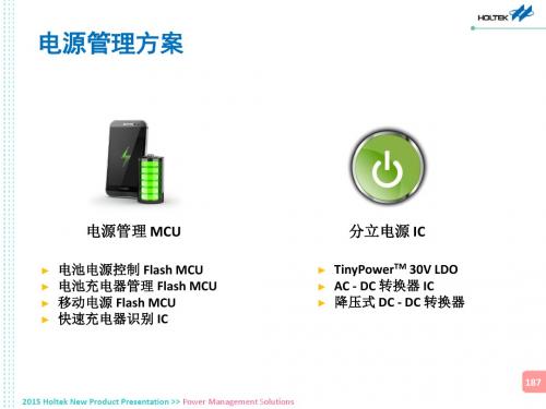
产品系列
Flash
HT45F3430
新产品
2K
2K16 ROM 1288 RAM 648 EEPROM
H.R. PWM
LCD
HT45F3420
1K
1K16 ROM 648 RAM 328 EEPROM
H.R. PWM
引脚个数
8/10 16/24
H.R. PWM:高分辨率 PWM 190
方框图
HT45F5N
Analog HOLTEK 8-Bit MCU Core
Driver
A/D 12-bit14 OCP2 OUVP2
4 KW Flash Memory
256 Bytes SRAM 64 Bytes EEPROM fSYS OSC. : HIRC
Auto-Adjust H.R. PWM with slew rate control2
当前市场巨大并将会持续扩大
► ►
用于锂离子和镍氢电池供电产品 保护并延长电池寿命
►
►
提供恒压控制
提供恒流控制
高功率 LED 手电筒
电子烟
189
2015 Holtek New Product Presentation >> Power Management Solutions >> Battery Power Control Flash MCU
内部参考电压
提供 A/D 转换器稳定电源
H.R. PWM
高分辨率 PWM 高达 500kHz @ 8-bit 分辨率
保护特性
OCP 硬件保护 PGA 1x ~ 51x 大电流检测
功能高度集成
直接驱动 NMOS 仅需少量外部元器件
IBM Cognos Transformer V11.2 用户指南说明书

User Guide
IBM
©
Product Information
This document applies to IBM Cognos Analytics version 11.2.0 and may also apply to subsequent releases.
• Linux is a registered trademark of Linus Torvalds in the United States, other countries, or both. • UNIX is a registered trademark of The Open Group in the United States and other countries. • Java and all Java-based trademarks and logos are trademarks or registered trademarks of Oracle and/or its affiliates.
The following terms are trademarks or registered trademarks of other companies:
• Adobe, the Adobe logo, PostScript, and the PostScript logo are either registered trademarks or trademarks of Adobe Systems Incorporated in the United States, and/or other countries.
Contents
Richtek RT8057 DS8057-04 February 2014 数据手册说明书

RT8057®©Copyright 2014 Richtek Technology Corporation. All rights reserved. is a registered trademark of Richtek Technology Corporation.Pin ConfigurationsOrdering InformationNote :Richtek products are :❝ RoHS compliant and compatible with the current require-ments of IPC/JEDEC J-STD-020.❝ Suitable for use in SnPb or Pb-free soldering processes.(TOP VIEW)WDFN-6SL 2x22.25MHz 1A Synchronous Step-Down ConverterGeneral DescriptionThe RT8057 is a high efficiency Pulse-Width-Modulated (PWM) step-down DC/DC converter, capable of delivering 1A output current over a wide input voltage range from 2.7V to 5.5V. The RT8057 is ideally suited for portable electronic devices that are powered from 1-cell Li-ion battery or from other power sources such as cellular phones, PDAs, hand-held devices, game console and related accessories.The internal synchronous rectifier with low R DS(ON)dramatically reduces conduction loss at PWM mode.No external Schottky diode is required in practical applications. The RT8057 enters Low Dropout Mode when normal Pulse -Width Mode cannot provide regulated output voltage by continuously turning on the upper P-MOSFET .The RT8057 enters shut-down mode and consumes less than 1μA when the EN pin is pulled low. The switching ripple is easily smoothed-ou t by small package filtering elements due to a fixed operating frequency of 2.25MHz.The RT8057 is available in a small WDFN-6SL 2x2 package.Features●2.7V to 5.5V Wide Input Operation Range●2.25MHz Fixed-Frequency PWM Operation ●Up to 1A Output Current ●Up to 90% Efficiency●0.6V Reference Allows Low Output Voltage ●Internal Soft-Start●No Schottky Diode Required●Internal Compensation to Reduce External Components●Low Dropout Operation : 100% Duty Cycle ●RoHS Compliant and Halogen FreeApplications●Portable Instruments●Game Console and Accessories●Microprocessors and DSP Core Supplies ●Cellular Phones●Wireless and DSL Modems ●PC CardsLXNC GND VIN ENFBJ7 : Product CodeW : Date CodeG : Green (Halogen Free and Pb Free)RT8057©Copyright 2014 Richtek Technology Corporation. All rights reserved. is a registered trademark of Richtek Technology Corporation.Function Pin DescriptionFunction Block DiagramTypical Application CircuitOUT 2.3VRT8057©Copyright 2014 Richtek Technology Corporation. All rights reserved. is a registered trademark of Richtek Technology Corporation.Absolute Maximum Ratings (Note 1)●Supply Input Voltage, V IN ------------------------------------------------------------------------------------------------6.5V ●Power Dissipation, P D @ T A = 25°CWDFN-6SL 2x2------------------------------------------------------------------------------------------------------------0.606W ●Package Thermal Resistance (Note 2)WDFN-6SL 2x2, θJA -------------------------------------------------------------------------------------------------------165°C/W WDFN-6SL 2x2, θJC ------------------------------------------------------------------------------------------------------8.2°C/W ●Lead Temperature (Soldering, 10 sec.)-------------------------------------------------------------------------------260°C ●Junction T emperature -----------------------------------------------------------------------------------------------------150°C●Storage T emperature Range --------------------------------------------------------------------------------------------−65°C to 150°C ●ESD Susceptibility (Note 3)HBM --------------------------------------------------------------------------------------------------------------------------2kV MM ----------------------------------------------------------------------------------------------------------------------------200VRecommended Operating Conditions (Note 4)●Supply Input Voltage, V IN ------------------------------------------------------------------------------------------------2.7V to 5.5V ●Junction T emperature Range --------------------------------------------------------------------------------------------−40°C to 125°C ●Ambient T emperature Range --------------------------------------------------------------------------------------------−40°C to 85°CElectrical CharacteristicsRT8057©Copyright 2014 Richtek Technology Corporation. All rights reserved. is a registered trademark of Richtek Technology Corporation.Note 1. Stresses beyond those listed “Absolute Maximum Ratings ” may cause permanent damage to the device. These are stressratings only, and functional operation of the device at these or any other conditions beyond those indicated in the operational sections of the specifications is not implied. Exposure to absolute maximum rating conditions may affect device reliability.Note 2. θJA is measured in natural convection at T A = 25°C on a low-effective thermal conductivity test board of JEDEC 51-3 thermalmeasurement standard. The measurement case position of θJC is on the exposed pad of the package.Note 3. Devices are ESD sensitive. Handling precaution is recommended.Note 4. The device is not guaranteed to function outside its operating conditions.Note 5. The reference voltage accuracy is ±2.5% at recommended ambient temperature range, guaranteed by design.RT8057©Copyright 2014 Richtek Technology Corporation. All rights reserved. is a registered trademark of Richtek Technology Corporation.Typical Operating CharacteristicsOutput Voltage vs. Input Voltage2.222.242.262.282.302.322.342.362.382.53.03.54.04.55.05.5Input Voltage (V)O u t p u t V o l t a g e (V)Efficiency vs. Output Current01020304050607080901000.00.20.40.60.81.0Output Current (A)E f f i c i e n c y (%)Frequency vs. Input Voltage2.002.052.102.152.202.252.302.352.402.53.03.54.04.55.05.5Input Voltage (V)F r e q u e n c y(M H z )Output Current Limit vs. Input Voltage1.01.11.21.31.41.51.62.53.03.54.04.55.05.5Input Voltage (V)O u t p u t C u r r e n t l im i t (A )Frequency vs. Temperature1.901.952.002.052.102.152.202.252.30-50-25255075100125Temperature (°C)F r e q u e n c y (M H z )Output Current Limit vs. Temperature1.01.11.21.31.41.51.6-50-25255075100125Temperature (°C)O u t p u t C u r r e n t Li m i t (A )RT8057©Copyright 2014 Richtek Technology Corporation. All rights reserved. is a registered trademark of Richtek Technology Corporation.Reference Voltage vs. Temperature0.5920.5940.5960.5980.6000.6020.6040.6060.608-50-25255075100125Temperature (°C)R e f e r e n c e V o l t a g e (V)Load Transient Response Time (100μs/Div)V IN = 5V, V OUT = 2.3V,I OUT = 0A to 1AI OUT(500mA/Div)V OUT(100mV/Div) Output RippleV IN = 3.3V, V OUT = 2.3V,I OUT = 1ATime (250ns/Div)V LX (5V/Div)V OUT (5mV/Div)Load Transient ResponseTime (100μs/Div)I OUT(500mA/Div)V OUT(100mV/Div)V IN = 5V, V OUT = 2.3V,I OUT = 0.4A to 1AOutput Voltage vs. Temperature2.252.262.272.282.292.302.312.322.332.342.35-50-25255075100125Temperature (°C)O u t p u t V o l t a g e (V)Output Ripple Time (250ns/Div)V LX (5V/Div)V OUT (5mV/Div)V IN = 5V, V OUT = 2.3V, I OUT = 1ART8057©Copyright 2014 Richtek Technology Corporation. All rights reserved. is a registered trademark of Richtek Technology Corporation.En Threshold vs. Temperature0.600.620.640.660.680.700.720.740.760.780.80-50-25255075100125Temperature (°C)E N T h r e s h o l d (V )UVLO vs. Temperature1.51.61.71.81.92.02.12.22.32.4-50-25255075100125Temperature (°C)U V L O (V)Power On from ENTime (100μs/Div)V EN (2V/Div)V OUT (2V/Div)I OUT(500mA/Div)V IN = 5V, V OUT = 2.3V,I OUT = 1APower Off from ENTime (100μs/Div)V EN (2V/Div)V OUT (2V/Div)I OUT(500mA/Div)V IN = 5V, V OUT = 2.3V,I OUT = 1AOutput Voltage vs. Output Current2.262.272.282.292.302.312.322.332.340.00.10.20.30.40.50.60.70.80.91.0Output Current (A)O u t p u t V o lt a g e (V )RT8057©Copyright 2014 Richtek Technology Corporation. All rights reserved. is a registered trademark of Richtek Technology Corporation.Application InformationThe basic RT8057 application circuit is shown in Typical Application Circuit. External component selection is determined by the maximum load current and begins with the selection of the inductor value and operating frequency followed by C IN and C OUT .Output Voltage SettingThe output voltage is set by an external resistive divider according to the following equation :OUT REFR1V V x (1)R2=+where VREF equals to 0.6V typical. The resistive divider allows the FB pin to sense a fraction of the output voltage as shown in Figure 1.Figure 1. Setting the Output VoltageSoft-StartThe RT8057 contains an internal soft-start clamp that gradually raises the clamp on the FB pin.100% Duty Cycle OperationWhen the input supply voltage decreases toward the output voltage, the duty cycle increases toward the maximum on-time. Further reduction of the supply voltage forces the main switch to remain on for more than one cycle,eventually reaching 100% duty cycle.The output voltage will then be determined by the input voltage minus the voltage drop across the internal P-MOSFET and the inductor.Low Supply OperationThe RT8057 is designed to operate down to an input supply voltage of 2.7V. One important consideration at low input supply voltages is that the R DS(ON) of the P-Channel and N-Channel power switches increases. The user should calculate the power dissipation when the RT8057 is used at 100% duty cycle with low input voltages to ensure that thermal limits are not exceeded.Under Voltage Protection (UVP)The output voltage can be continuously monitored for under voltage protection. When the output voltage is less than 33% of its set voltage threshold after OCP occurs, the under voltage protection circuit will be triggered to auto re-soft-start.Input Voltage Over Voltage protection (V IN OVP)When the input voltage (V IN ) is higher than 6V, V IN OVP will be triggered and the IC stops switching. Once the input voltage drops below 6V, the IC will return to normal operation.Output Over Voltage Protection (V OUT OVP)When the output voltage exceeds more than 5% of the nominal reference voltage, the feedback loop forces the internal switches off within 50μs. Therefore, the output over voltage protection is automatically triggered by the loop.Short Circuit ProtectionWhen the output is shorted to ground, the inductor current decays very slowly during a single switching cycle. A current runaway detector is used to monitor inductor current. As current increases beyond the control of current loop, switching cycles will be skipped to prevent current runaway from occurring.RT8057©Copyright 2014 Richtek Technology Corporation. All rights reserved. is a registered trademark of Richtek Technology Corporation.C IN and C OUT SelectionThe input capacitance, C IN , is needed to filter the trapezoidal current at the source of the top MOSFET . To prevent large ripple voltage, a low ESR input capacitor sized for the maximum RMS current should be used. RMScurrent is given by :RMS OUT(MAX)I I =This formula has a maximum at V IN = 2V OUT , where I RMS =I OUT /2. This simple worst case condition is commonly used for design because even significant deviations do not result in much difference. Choose a capacitor rated at a higher temperature than required.Several capacitors may also be paralleled to meet size or height requirements in the design.The selection of C OUT is determined by the effective series resistance (ESR) that is required to minimize voltage ripple and load step transients, as well as the amount of bulk capacitance that is necessary to ensure that the control loop is stable. Loop stability can be checked by viewing the load transient response. The output ripple, ΔV OUT , is determined by :OUT L OUT 1V I ESR 8fC ⎡⎤∆≤∆+⎢⎥⎣⎦The output ripple is highest at maximum input voltagesince ΔI L increases with input voltage. Multiple capacitors placed in parallel may be needed to meet the ESR andRMS current handling requirements. Dry tantalum, special polymer, aluminum electrolytic and ceramic capacitors are all available in surface mount packages. Special polymer capacitors offer very low ESR, but have lower capacitance density than other types. Tantalum capacitors have the highest capacitance density, but it is important to only use types that have been surge tested for use in switching power supplies. Aluminum electrolytic capacitors have significantly higher ESR, but can be used in cost-sensitive applications provided that consideration is given to ripple current ratings and long term reliability. Ceramic capacitors have excellent low ESR characteristics, but can have a high voltage coefficient and audible piezoelectric effects.The high Q of ceramic capacitors with trace inductance can also lead to significant ringing.Using Ceramic Input and Output CapacitorsHigher value, lower cost ceramic capacitors are now becoming available in smaller case sizes. Their high ripple current, high voltage rating and low ESR make them ideal for switching regulator applications. However, care must be taken when these capacitors are used at the input and output. When a ceramic capacitor is used at the input and the power is supplied by a wall adapter through long wires, a load step at the output can induce ringing at the input, V IN . At best, this ringing can couple to the output and be mistaken as loop instability. At worst, a sudden inrush of current through the long wires can potentially cause a voltage spike at V IN large enough to damage the part.Table 2. Capacitors for C IN and C OUTRT8057©Copyright 2014 Richtek Technology Corporation. All rights reserved. is a registered trademark of Richtek Technology Corporation.Thermal ConsiderationsFor continuous operation, do not exceed absolute maximum junction temperature. The maximum power dissipation depends on the thermal resistance of the IC package, PCB layout, rate of surrounding airflow, and difference between junction and ambient temperature. The maximum power dissipation can be calculated by the following formula :P D(MAX) = (T J(MAX) − T A ) / θJAwhere T J(MAX) is the maximum junction temperature, T A is the ambient temperature, and θJA is the junction to ambient thermal resistance.For recommended operating condition specifications of the RT8057, the maximum junction temperature is 125°C and T A is the ambient temperature. The junction to ambient thermal resistance, θJA , is layout dependent. For WDFN-6SL 2x2 packages, the thermal resistance, θJA , is 165°C/W on a standard JEDEC 51-3 single-layer thermal test board. The maximum power dissipation at T A = 25°C can be calculated by the following formula :P D(MAX) = (125°C − 25°C) / (165°C/W) = 0.606W for WDFN-6SL 2x2 packageThe maximum power dissipation depends on the operating ambient temperature for fixed T J(MAX) and thermal resistance, θJA . For the RT8057 package, the derating curve in Figure 2 allows the designer to see the effect of rising ambient temperature on the maximum power dissipation.Figure 2. Derating Curve for the RT8057 PackageLayout ConsiderationsFollow the PCB layout guidelines for optimal performance of the RT8057.❝ Connect the terminal of the input capacitor(s), C IN , asclose as possible to the VIN pin. This capacitor provides the AC current into the internal power MOSFETs.❝ LX node experiences high frequency voltage swing andshould be kept within a small area. Keep all sensitive small-signal nodes away from the LX node to prevent stray capacitive noise pick up.❝ Flood all unused areas on all layers with copper. Floodingwith copper will reduce the temperature rise of power components. Connect the copper areas to any DC net (V IN , V OUT , GND, or any other DC rail in the system).❝ Connect the FB pin directly to the feedback resistors.The resistive voltage divider must be connected between V OUT and GND.Figure 3. PCB Layout GuideINLX should be connected to inductor by wide and short trace. Keep sensitive 0.000.050.100.150.200.250.300.350.400.450.500.550.600.650255075100125Ambient Temperature (°C)M a x i m u m P o w e r D i s s i p a t i o n (W )W-Type 6SL DFN 2x2 PackageRichtek Technology Corporation14F, No. 8, Tai Yuen 1st Street, Chupei CityHsinchu, Taiwan, R.O.C.Tel: (8863)5526789Richtek products are sold by description only. Richtek reserves the right to change the circuitry and/or specifications without notice at any time. Customers should obtain the latest relevant information and data sheets before placing orders and should verify that such information is current and complete. Richtek cannot assume responsibility for use of any circuitry other than circuitry entirely embodied in a Richtek product. Information furnished by Richtek is believed to be accurate and reliable. However, no responsibility is assumed by Richtek or its subsidiaries for its use; nor for any infringements of patents or other rights of third parties which may result from its use. No license is granted by implication or otherwise under any patent or patent rights of Richtek or its subsidiaries.DS8057-04 February 11。
随机利率下基于蒙特卡洛算法的巨灾保险破产概率模拟
2021年5月第30卷第2期中央民族大学学报(自然科学版)Journal of MUC( Natural Sciences Edition)May, 2021Vol. 30 No. 2随机利率下基于蒙特卡洛算法的巨灾保险破产概率模拟巢文\钱晓涛2(1.福建工程学院管理学院,福州350118; 2.阳光学院基础教研部,福州350015)摘要:巨灾保险是分散巨灾风险的一种重要手段,而破产概率则是评估保险公司巨灾风险偿付能力的一个关键数量指标。
在利率服从C1R随机利率模型且巨灾索赔服从对数正态分布的假设下,本文采用经典更新风险模型描述保险公司盈余过程,并应用蒙特卡洛算法估计保险公司经营巨灾风险的破产概率,利用Mat-l a b软件进行了模拟,所得结果验证了基于蒙特卡洛算法估计随机利率下巨灾保险破产概率方案的有效性和可行性。
关键词:巨灾保险;随机利率;蒙特卡洛算法;破产概率中图分类号:0211.9 文献标识码:A文章编号=1005-8036(2021) 02-0047-05我国是世界上受自然灾害影响最严重的国家之一。
随着经济水平的发展,巨灾造成的经济损失呈 现明显上升趋势。
然而,由于国内整体上巨灾风险防范意识薄弱,再加上巨灾风险分散技术的限制,巨灾保险在分散巨灾风险时的作用非常有限,造成我国巨灾保险供给缺口严重。
建立完善的巨灾保险制 度是实现分散巨灾风险,促进巨灾保险供给的重要渠道[1<。
保险公司作为巨灾保险制度的主要支柱,其破产概率是分析保险公司经营巨灾风险能力的一个重要数量指标。
由巨灾引起的“大索赔”需要用重尾分布来刻画,这导致巨灾保险的破产概率不具有显式表达式。
目前,已经有许多学者研究了“大索赔”下破产概率的渐近结果〜8],蒙特卡洛算法也被应用到巨灾保险 破产概率和再保险定价的模拟中纵观上述研究,大部分都局限在巨灾索赔服从正则变化尾分布的范围,或者未考虑利率因素尤其是随机利率。
鉴于此,本文应用蒙特卡洛算法模拟随机利率下巨灾保 险的破产概率,其中巨灾索赔服从非正则变化尾分布,所得结果可以为保险公司稳定经营巨灾风险进一 步提供技术支持。
商品说明书:X2背部 顶部 侧部 底部视图
Professional Display Solutions
* ** *
LED display controller
optional accessories Power plug types vary by country/region.
Plug the power plug into the electric outlet only when the cables are properly wired. Note: More cable wiring scheme and mounting scheme can be found in the User’s Manual.
CTN: BM907005
Optional accessory CTN: BM907000
Not included
T style inner hexagon wrench, size 7
4 Connecting the data and power cables
X1
LAN cable Power cable (daisy chain)
Rear/top/side/bottom views
LAN cable (RJ45, CAT-5): 2 pcs
Power cable (daisy chain): 2 pcs
Quick start guide: 1 pcs
* Di erences according to regions. Display design and accessories may di er from those illustrated above.
2
1 POWER IN connector 2 POWER OUT connector 3 DATA connector 4 DATA connector
8 Multi-function Compact Inverter MX2-Series V1型型号
Born to drive machines•Positioning functionality.•Fieldbus communications with optional unit EtherCAT, CompoNet and DeviceNet •Drive Programming.•Current vector Control.•High Starting torque: 200% at 0.5 Hz.•Safety function * EN ISO 13849-1:2008 (Cat.3/PLd)IEC 60204-1 Stop Category 0•Speed range up to 580 Hz.*When optional DeviceNet communication unit or CompoNet communication unit is mounted onto the MX2-series V1 type, the inverter will not conform to the safety standards.Performance SpecificationsInverter MX2-series V1 type3-phase 200 V Class*The BRD usage is 10%.Function name3-phase 200 VModel name (3G3MX2-)A2001-V1A2002-V1A2004-V1A2007-V1A2015-V1A2022-V1A2037-V1A2055-V1A2075-V1A2110-V1A2150-V1Applicable motor capacity kW CT 0.10.20.40.75 1.5 2.2 3.7 5.57.51115VT 0.20.40.75 1.1 2.2 3.0 5.57.5111518.5HP CT 1/81/41/212357 1/2101520VT 1/41/21 1 1/2347 1/210152025Rated output capacity [kVA]200 V CT 0.20.5 1.0 1.7 2.7 3.8 6.08.611.416.220.7VT 0.40.6 1.2 2.0 3.3 4.1 6.710.313.819.323.9240 VCT 0.30.6 1.2 2.0 3.3 4.57.210.313.719.524.9VT0.40.7 1.4 2.4 3.9 4.98.112.416.623.228.6Rated input voltage 3-phase 200 V - 15% to 240 V + 10%, 50/60 Hz ± 5%Rated input current [A]CT1.0 1.6 3.3 6.09.012.720.530.839.657.162.6VT 1.2 1.93.97.210.813.923.037.048.068.072.0Rated output voltage 3-phase 200 to 240 V (The output cannot exceed the incoming voltage).Rated output current [A]CT 1.0 1.6 3.0 5.08.011.017.525.033.047.060.0VT1.2 1.9 3.5 6.09.612.019.630.040.056.069.0Short-time deceleration braking torque (%)(Discharge Resistor not connected)5050505050202020201010Braking Resistor circuit *Regenerative brakingBuilt-in Braking Resistor circuit (separate Discharge Resistor)Min. connectable resistance [Ω]1001001005050353520171710Weight [kg]1.01.01.11.21.61.82.03.33.45.17.4Dimensions (width × height) [mm]68 × 128108 × 128140 × 128140 × 260180 × 296220 × 350Dimensions (depth) [mm]109122.5145.5170.5170.5155175Multi-function Compact Inverter MX2-Series V1 type3-phase 400 V Class*The BRD usage is 10%.1-phase 200 V Class*The BRD usage is 10%.Function name3-phase 400 VModel name (3G3MX2-)A4004-V1A4007-V1A4015-V1A4022-V1A4030-V1A4040-V1A4055-V1A4075-V1A4110-V1A4150-V1Applicable motor capacity kW CT 0.40.75 1.5 2.2 3.0 4.0 5.57.51115VT 0.75 1.5 2.2 3.0 4.0 5.57.5111518.5HP CT 1/2123457 1/2101520VT 123457 1/210152025Rated output capacity [kVA]380 V CT 1.1 2.2 3.1 3.6 4.7 6.09.711.815.720.4VT 1.3 2.6 3.5 4.5 5.77.311.515.120.425.0480 VCT 1.4 2.8 3.9 4.5 5.97.612.314.919.925.7VT1.7 3.4 4.4 5.77.39.214.519.125.731.5Rated input voltage 3-phase 380 V - 15% to 480 V + 10%, 50/60 Hz ± 5%Rated input current [A]CT1.8 3.6 5.2 6.57.711.016.918.829.435.9VT2.1 4.3 5.98.19.413.320.024.038.044.0Rated output voltage 3-phase 380 to 480 V (The output cannot exceed the incoming voltage).Rated output current [A]CT 1.8 3.4 4.8 5.57.29.214.818.024.031.0VT2.1 4.1 5.4 6.98.811.117.523.031.038.0Short-time deceleration braking torque (%)(Discharge Resistor not connected)50505020202020201010Braking Resistor circuit *Regenerative brakingBuilt-in Braking Resistor circuit (separate Discharge Resistor)Min. connectable resistance [Ω]18018018010010010070707035Weight [kg]1.51.61.8 1.91.92.13.53.54.75.2Dimensions (width × height) [mm]108 × 128140 × 128140 × 260180 × 296Dimensions (depth) [mm]143.5170.5170.5155175Function name1-phase 200 V Model name (3G3MX2-)AB001-V1AB002-V1AB004-V1AB007-V1AB015-V1AB022-V1Applicable motor capacity kW CT 0.10.20.40.75 1.5 2.2VT 0.20.40.55 1.1 2.2 3.0HP CT 1/81/41/2123VT 1/41/23/4 1 1/234Rated output capacity [kVA]200 V CT 0.20.5 1.0 1.7 2.7 3.8VT 0.40.6 1.2 2.0 3.3 4.1240 VCT 0.30.6 1.2 2.0 3.3 4.5VT0.40.7 1.4 2.4 3.9 4.9Rated input voltage 1-phase 200 V - 15% to 240 V + 10%, 50/60 Hz ± 5%Rated input current [A]CT 1.3 3.0 6.311.516.822.0VT 2.0 3.67.313.820.224.0Rated output voltage 3-phase 200 to 240 V (The output cannot exceed the incoming voltage).Rated output current [A]CT 1.0 1.6 3.0 5.08.011.0VT1.2 1.9 3.5 6.09.612.0Short-time deceleration braking torque (%)(Discharge Resistor not connected)505050505020Braking Resistor circuit *Regenerative brakingBuilt-in Braking Resistor circuit (separate Discharge Resistor)Min. connectable resistance [Ω]100100100505035Weight [kg]1.01.0 1.11.61.8 1.8Dimensions (width × height) [mm]68 × 128108 × 128Dimensions (depth) [mm]109122.5170.5Multi-function Compact Inverter MX2-Series V1 typeFunction SpecificationsFunction nameSpecificationsEnclosure ratings *1Open type (IP20)C o n t r o lControl methodPhase-to-phase sinusoidal modulation PWMOutput frequency range *20.10 to 400 Hz (or 580 Hz in the high-frequency mode; restrictions apply)Frequency precision *3Digital command: ±0.01% of the max. frequency, Analog command: ±0.2% of the max. frequency (25±10°C)Frequency setting resolution Digital setting: 0.01 Hz, Analog setting: One-thousandth of the maximum frequency Voltage/Frequency characteristics V/f characteristics (constant/reduced torque)Sensorless vector control, V/f control with speed feedback Overload current rating Heavy load rating (CT): 150%/60 s Light load rating (VT): 120%/60 sInstantaneous overcurrent protection200% of the value of heavy load rating (CT)Acceleration/Deceleration time 0.01 to 3600 s (linear/curve selection), acceleration/deceleration 2 setting available Carrier frequency adjustment range 2 to 15 kHz (with derating)Starting torque200%/0.5 Hz (sensorless vector control)External DC injection brakingStarts at a frequency lower than that in deceleration via the STOP command, at a value set lower than that during operation, or via an external input. (Level and time settable).Protective functionsOvercurrent, overvoltage, undervoltage, electronic thermal, temperature error, ground fault overcur-rent at power-on status, rush current prevention circuit, overload limit, incoming overvoltage, exter-nal trip, memory error, CPU error, USP error, communication error, overvoltage suppression during deceleration, protection upon momentary power outage, emergency cutoff, etc.I n p u t s i g n a l Frequency settings Digital OperatorExternal analog input signal: 0 to 10 VDC/4 to 20 mA, Modbus communication (Modbus-RTU)RUN/STOP command Digital OperatorExternal digital input signal (3-wire input supported), Modbus communication (Modbus-RTU)Multi-function input 7 points (Selectable from 59 functions)Analog input 2 points (Voltage FV terminal: 10 bits/0 to 10 V, Current FI terminal: 10 bits/4 to 20 mA)Pulse input1 point (RP terminal: 32 kHz max., 5 to 24 VDC)O u t p u t s i g n a l Multi-function output 2 points (P1/EDM, P2; selectable from 43 functions)Relay output 1 point (1c contact: MC, MA, MB; selectable from 43 functions)Analog output (Frequency monitor) 1 point (AM terminal: Voltage 10 bits/0 to 10 V) (Frequency, current selectable)Pulse output 1 point (MP terminal: 32 kHz max., 0 to 10 V)C o m m u n i c a t i o n s RS-422RJ45 connector (for Digital Operator)RS-485Control circuit terminal block, Modbus communication (Modbus-RTU)USBUSB1.1, mini-B connectorDrive Programming *4Calculate, Logic, Control I/O and so onOther functionsAVR function, V/f characteristics switching, upper/lower limit, 16-step speeds, starting frequency adjustment, jogging operation, carrier frequency adjustment, PID control, frequency jump, analog gain/bias adjustment, S shape acceleration/deceleration, electronic thermal characteristics, level adjustment, restart function, torque boost function, fault monitor, soft lock function, frequencyconversion display, USP function, motor 2 control function, UP/DWN, overcurrent control function, etc.O p e r a t i n g e n v i r o n m e n t Ambient operating temperature -10 to 50°C (However, derating is required).Ambient storage temperature -20°C to 65°CAmbient operating humidity 20% to 90% RH (with no condensation)Vibration resistance 5.9 m/s 2 (0.6G), 10 to 55 HzApplication environment At a maximum altitude of 1,000 m; indoors (without corrosive gases or dust)O p t i o n sEtherCAT Communication Unit 3G3AX-MX2-ECT CompoNet Communication Unit 3G3AX-MX2-CRT-E DeviceNet Communication Unit3G3AX-MX2-DRT-EMulti-function Compact Inverter MX2-Series V1 type*1Protection method complies with JEM 1030.*2To operate the motor at over 50/60 Hz, contact the motor manufacturer to find out the maximum allowable speed of revolution.*3For the stable control of the motor, the output frequency may exceed the maximum frequency set in A004 (A204) by 2 Hz max.*4Refer to the Drive Programming USER'S MANUAL (No. I580).Note:1.The applicable motor is a 3-phase standard motor. For using any other type, be sure that the rated current does not exceed that of the Inverter.2.Output voltage decreases according to the level of the power supply voltage.3.The braking torque at the time of capacitor feedback is an average deceleration torque at the shortest deceleration (when it stops from 50 Hz). It is not a continuous regeneration torque. Also, the average deceleration torque varies depending on the motor loss. The value is reduced in operation over 50 Hz.Other option DC reactor, AC reactor, radio noise filter, input noise filter, output noise filter, regenerative braking unit, Braking Resistor, etc.I n t e r n a t i o n a l s t a n d a r dECdirectiveEMC directiveEN61800-3: 2004Low voltage directiveEN61800-5-1: 2007Machinery directivesIEC 60204-1 Stop Category 0, EN IEC 61800-5-2 (STO), EN ISO 13849-1: 2008 (PLd)UL/cULUL508CFunction nameSpecificationsMulti-function Compact Inverter MX2-Series V1 typeComponents and FunctionsInverter MX2-series V1 typeNote:This illustration shows the terminal block with the front cover removed.Name FunctionModbus-RTU Termination resistor selector switch Use this Terminal Resistor selector switch for RS-485 terminals on the control circuit terminal block. When this switch is turned ON, the internal 200 Ω Resistor is connected. Safety function selector switch Turn this switch ON when using the safety function. Turn OFF the power before turning this switch ON/OFF. For details, refer to USER’S MANUAL (Cat.No.I585).EDM function selector switch Turn this switch ON when using the EDM output of the safety function. Turn OFF the power before turning this switch ON/OFF.For details, refer to USER’S MANUAL (Cat.No.I585).USB connectorUse this mini-B USB connector to connect a PC.Even when the Inverter is being operated by a PC, etc., via USB connection, it can still be operated using the Digital Operator.Connector for Digital Operator Use this connector to connect the Digital Operator.Connector for optional board Use this connector to mount the optional board. (Communications Units and other options can be connected.) Control circuit terminal blocks A and BThese terminal blocks are used to connect various digital/analog input and output signals for inverter control, etc. Multi-function contact terminal block Use this SPDT contact terminal block for relay outputs.Main circuit terminal block Use this terminal block to connect an output to the motor and Braking Resistor, etc.Also, use this terminal block to connect the inverter to the main power supply.CHARGE indicator (Charge indicator LED)This LED indicator is lit if the DC voltage of the main circuit (between terminals P/+2 and N/-) remains approx. 45 V or above after the power has been cut off. Before wiring, etc. confirm that the Charge LED indicator is turned OFF.Multi-function Compact Inverter MX2-Series V1 typeConnection DiagramDimensions(Unit: mm)Single-phase 3-phase power supply*1 Connect to terminals L1 and N on a single-phase, 200-V Inverter (3G3MX2-AB @@@-V1).*2 Optional.3G3MX2-AB001-V13G3MX2-AB002-V13G3MX2-AB004-V13G3MX2-A2001-V13G3MX2-A2002-V13G3MX2-A2004-V13G3MX2-A2007-V1Power supply ModelW [mm]H [mm] D [mm]D1 [mm]1-phase 200 V3G3MX2-AB001-V13G3MX2-AB002-V16812810913.53G3MX2-AB004-V1122.5273-phase 200 V3G3MX2-A2001-V13G3MX2-A2002-V110913.53G3MX2-A2004-V1122.5273G3MX2-A2007-V1145.550Multi-function Compact Inverter MX2-Series V1 type3G3MX2-AB007-V13G3MX2-AB015-V13G3MX2-AB022-V13G3MX2-A2015-V13G3MX2-A2022-V13G3MX2-A4004-V13G3MX2-A4007-V13G3MX2-A4015-V13G3MX2-A4022-V13G3MX2-A4030-V1Power supply ModelW [mm]H [mm] D [mm]D1 [mm]1-phase 200 V3G3MX2-AB007-V13G3MX2-AB015-V13G3MX2-AB022-V1108128170.5553-phase 200 V 3G3MX2-A2015-V13G3MX2-A2022-V13-phase 400 V3G3MX2-A4004-V1143.5283G3MX2-A4007-V13G3MX2-A4015-V13G3MX2-A4022-V13G3MX2-A4030-V1170.5553G3MX2-A2037-V13G3MX2-A4040-V1Power supplyModelW [mm]H [mm] D [mm]D1 [mm]3-phase 200 V 3G3MX2-A2037-V1140128170.5553-phase 400 V3G3MX2-A4040-V13G3MX2-A2055-V13G3MX2-A2075-V13G3MX2-A4055-V13G3MX2-A4075-V1Power supplyModelW [mm]H [mm] D [mm]D1 [mm]3-phase 200 V 3G3MX2-A2055-V13G3MX2-A2075-V114026015573.33-phase 400 V3G3MX2-A4055-V13G3MX2-A4075-V1。
2015GSMC_MPW_Timetable
Tech/Date Jan.Feb.Mar.Apr.May.Jun.Jul.Aug.Sep.Oct.Nov.Dec.0.028um IO=1.8V| IO=2.5VCMOS Logic (GP|LP)17MZP(F8)02MZW(F8)0.04um IO=1.8/2.5V| IO=1.8V|IO=2.5V CMOS Logic(LL)24MZR(F8)05Q03(F8)0.055um IO=1.8/2.5/5V|IO=1.8/2.5V|IO=1.8/3.3/5V|IO=1.8/3.3V| IO=1.8/5V|IO=1.8V| IO=2.5/5V|IO=2.5V| IO=3.3/5V|IO=3.3V Adv.Emb-Flash (Cu-BEOL)(LL)24MZL(B1)16MZX(B1)0.055um IO=1.8/2.5V|IO=1.8/3.3V| IO=1.8V|IO=2.5V| IO=3.3VCMOS Logic (LL)20MZM(B1)24MZS(B1)19Q04(B1)0.065um IO=1.8/2.5V|IO=1.8/3.3V|IO=1.8V|IO=2.5V|IO=3.3VCMOS Logic (LL)20MZM(B1)24MZS(B1)19Q04(B1)0.065um IO=1.8/2.5V|IO=1.8/3.3V|IO=1.8V|IO=2.5V|IO=3.3VMixed Signal (LL)20MZM(B1)24MZS(B1)19Q04(B1)0.11um IO=3.3VCMOS Logic (GE)17MZT(S1)30Q09(S1)0.11um IO=3.3VMixed Signal (GE)17MZT(S1)30Q09(S1)0.13um IO=3.3/5V|IO=5VAdv. emb-EEPROM(Cu-BEOL) (LL)31MZU(S1)0.13um IO=3.3/5VAdv. emb-Flash (Cu-BEOL) (LL)12MZZ(S1)0.13um IO=3.3VCMOS Logic (GE)24MZQ(S1)28MZY(S1)0.13um IO=3.3VMixed Signal (GE)24MZQ(S1)28MZY(S1)0.153um IO=3.3VCMOS Logic (GE)26Q05(S1)SMIC 2015 MPW Booking Cutoff DateTech/Date Jan.Feb.Mar.Apr.May.Jun.Jul.Aug.Sep.Oct.Nov.Dec.0.153um IO=3.3VMixed Signal (GE)26Q05(S1)0.18um IO=3.3VCMOS Logic (GE)27MZN(F7)10MZV(S1)14Q01(S1)19Q06(F7)23Q0B(F7)0.18um IO=3.3/5V|IO=5VEEPROM Embedded(GE)07Q02(S1)0.18um IO=3.3/5V|IO=5VEmbedded Flash (EM)09Q07(S1)0.18um IO=3.3V| IO=5VMixed Signal(GE|PM)27MZN(F7)10MZV(S1)10MZV(S1)5V14Q01(F7)19Q06(S1)19Q06(S1)5V23Q0B(F7)Tech/Date Jan.Feb.Mar.Apr.May.Jun.Jul.Aug.Sep.Oct.Nov.Dec.0.028um IO=1.8V| IO=2.5VCMOS Logic (GP|LP)08MYH(F8)23MZH(F8)11MZ7(F8)16MZG(F8)0.04um IO=1.8/2.5V| IO=1.8V|IO=2.5V CMOS Logic(LL)25MY5(F8)22MYD(F8)24MYN(F8)26MYX(F8)28MZ5(F8)23MZE(F8)0.055um IO=1.8/2.5/5V|IO=1.8/2.5V|IO=1.8/3.3/5V|IO=1.8/3.3V| IO=1.8/5V|IO=1.8V| IO=2.5/5V|IO=2.5V| IO=3.3/5V|IO=3.3V Adv.Emb-Flash (Cu-BEOL)(LL)31MZJ(B1)0.055um IO=1.8/2.5V|IO=1.8/3.3V| IO=1.8V|IO=2.5V| IO=3.3VCMOS Logic (LL)13MY3(B1)08MYB(B1)10MYK(B1)12MYW(B1)07MZ1(B1)09MZC(B1)0.065um IO=1.8/2.5V|IO=1.8/3.3V|IO=1.8V|IO=2.5V|IO=3.3VCMOS Logic (LL)13MY3(B1)08MYB(B1)10MYK(B1)12MYW(B1)07MZ1(B1)09MZC(B1)0.065um IO=1.8/2.5V|IO=1.8/3.3V|IO=1.8V|IO=2.5V|IO=3.3VMixed Signal (LL)13MY3(B1)08MYB(B1)10MYK(B1)12MYW(B1)07MZ1(B1)09MZC(B1)0.11um IO=3.3VCMOS Logic (GE)18MY4(S1)6MYF(S1)29MYT(S1)14MZ3(S1)30MZF(S1)0.11um IO=3.3VMixed Signal (GE)18MY4(S1)6MYF(S1)29MYT(S1)14MZ3(S1)30MZF(S1)0.13um IO=3.3/5V|IO=5VAdv. emb-EEPROM(Cu-BEOL) (LL)15MY6(S1)01MYP(S1)4MZ6(S1)0.13um IO=3.3/5VAdv. emb-Flash (Cu-BEOL) (LL)07MY8(S1)05MYS(S1)25MZA(S1)0.13um IO=5VAdv. standalone-EEPROM (LL)15MY6(S1)0.13um IO=3.3VCMOS Logic (GE)14MY1(S1)18MY4(S1)02MY9(S1)06MYF(S1)17MYL(S1)29MYT(S1)09MYZ(S1)14MZ3(S1)18MZ9(S1)30MZF(S1)0.13um IO=3.3VCMOS Logic (LL)17MYL(S1)SMIC 2014 MPW Booking Cutoff Date0.13um IO=3.3VMixed Signal (GE)14MY1(S1)18MY4(S1)02MY9(S1)06MYF(S1)17MYL(S1)29MYT(S1)09MYZ(S1)14MZ3(S1)18MZ9(S1)30MZF(S1)0.13um IO=3.3VMixed Signal (LL)17MYL(S1)0.153um IO=3.3VCMOS Logic (GE)13MYG(S1)0.18LG/MS*85%shrinkage06MZK(B1)0.153um IO=3.3VCMOS Logic (GE)13MYG(S1)0.18LG/MS*85%shrinkage06MZK(B1)0.18um IO=3.3VCMOS Logic (GE)04MY2(F7)11MY7(S1)with0.18LG/MS1.8/5V15MYC(F7)20MYJ(S1)24MYM(F7)06MYU(S1)with0.18LG/MS1.8/5V09MYY(F7)14MZ2(S1)18MZ8(F7)23MZD(S1)with0.18LG/MS1.8/5V0.18um IO=3.3/5V|IO=5VEEPROM Embedded(GE)08MYA(S1)05MYV(S1)02MZB(S1)0.18um IO=3.3/5V|IO=5VEmbedded Flash (EM)06MYE(S1)21MZ4(S1)0.18um IO=3.3VMixed Signal (GE)04MY2(F7)11MY7(S1)with0.18LG/MS1.8/5V15MYC(F7)20MYJ(S1)24MYM(F7)06MYU(S1)with0.18LG/MS1.8/5V09MYY(F7)14MZ2(S1)18MZ8(F7)23MZD(S1)with0.18LG/MS1.8/5V0.18um IO=5VMixed Signal (PM)11MY7(S1)06MYU(S1)23MZD(S1)0.35um IO=3.3V|IO=5VEEPROM embedded(GE|HV)08MYQ(S1)0.35um IO=5V|IO=NAVMixed Signal (GE)15MYR(S1)Enhanceddesign ruleTD-MM35-DR-2002/S1。
- 1、下载文档前请自行甄别文档内容的完整性,平台不提供额外的编辑、内容补充、找答案等附加服务。
- 2、"仅部分预览"的文档,不可在线预览部分如存在完整性等问题,可反馈申请退款(可完整预览的文档不适用该条件!)。
- 3、如文档侵犯您的权益,请联系客服反馈,我们会尽快为您处理(人工客服工作时间:9:00-18:30)。
8
4
CUBIC PARAMETRIC CURVES
x = a31 u3 + a21 u2 + a11 u + a01 y = a32 u3 + a22 u2 + a12 u + a02 z = a33 u3 + a23 u2 + a13 u + a03 when 0 u 1
u=0 P0 T1 T0 P1 u=1
Z
M0601 L04 Curve Modeling
Q1 Q3
Q0 Q2
X
Y
16
8
MODIFICATION TO BÉZIER CURVE
FMDD-CAD 2015
By displacing one point, the curve is modified P’(u) = P(u) + D (u)
0.6
0.7
0.8
0.9
1.0
u
0
0.1
0.2
0.3
0.4
0.5
0.6
0.7
0.8
0.9
1.0
u
Hale Waihona Puke 13BÉZIER CURVES - EXAMPLES
Beziér demonstrator 01 - Linear interpolation 02 - Parametric curve 03 - The cubic Bézier curve 04 - Bézier properties 05 - de Casteljau’ algorithm 06 - Subdividing the Bézier curve 07 - Higher degree Bézier curves 08 - Bézier curve degree elevation 09 - Hermite interpolation > Bézier
M0601 L04 Curve Modeling
where P (u) = n i=0 Qi * Bi,n (u) D (u) = n i=0 D Qi * Bi,n (u)
Z
Q’2
Q1 Q2 Q0
X
Q3
Y
D Q2 * B2,3 (u0)
17
CONSIDERATIONS ON BÉZIER CURVES
FMDD-CAD 2015
POLITECNICO DI TORINO Automotive & Mechanical Engineering
Fundamentals of Mechanical Design & Drawing
M0601 L04 Curve Modeling
M0601 L04 CURVE MODELING
14
FMDD-CAD 2015
M0601 L04 Curve Modeling
7
THE BÉZIER CURVES PROPERTIES
The shape of the curve is a function of poles only Only the ends of the polygon belongs to the curve Tangents at the ends are parallel to the first and last section of the polygon Curvature at the ends depends therefore from the first and last three polygon vertices, respectively The curve lies within the convex polyhedron resulting from poles envelopment For convex polygon, the curve is convex too The shape does not change for transformations The formulation is of a global type
FMDD-CAD 2015
M0601 L04 Curve Modeling
P(u) = P0 F0(u) + P1 F1(u) + T0 G0(u) + T1 G1(u) when F0 = 2 u3 - 3 u2 + 1 F1 = -2 u3 + 3 u2 G0 = u3 - 2 u2 + u G1 = u3 - u2
Support the design and machining of complex “free-form” surfaces and related curves.
Solid models
Catch the 3D geometry of a solid object “as a whole” as an aid to higher functionality and automation levels than with other types of geometrical models.
F0(u) 1 G0(u) 0,15 0 -0,15 G1(u) u 1 F1(u)
9
SPLINE CURVE
FMDD-CAD 2015
Assembly of n continuous cubic parametric segments
interpolating n+1 control points Pk comply with continuity C0, C1 and C2 at junction point
4
2
THE PROBLEM
FMDD-CAD 2015
Open surfaces modeling (skins) Principal sectors
M0601 L04 Curve Modeling
Aviation Shipbuilding Automotive
Scope
Functional (aerodynamics, technological, etc.) Aesthetic
FMDD-CAD 2015
The method allows an intuitive approach for users expert of the problem, but not of the mathematical formulation
B
1.0 0.9 0.8 0.7 0.6 0.5 0.4 0.3 0.2 0.1 0 0 0.1 0.2 0.3 0.4 0.5 0.6 0.7 0.8 0.9 1.0
FMDD-CAD 2015
Case n = 3
Bernstein Polynomials
B0,3
B3,3
M0601 L04 Curve Modeling
x = X(u) y = Y(u) z = Z(u) when 0 u 1
Z P (u0) u=0 X 0 u0 1 u T (u0) u=1 Y
M0601 L04 Curve Modeling
When u changes within the interval considered, the corresponding point P(x, y, z) will plot a curve.
1D
2D
3D
7
PARAMETRIC CURVE
FMDD-CAD 2015
A curve is called parametric when coordinates of the current point can be expressed on it by analytic equation as a u parameter variable.
B
FMDD-CAD 2015
B0,3
Case n = 3
B3,3
1.0 0.9 0.8 0.7 0.6
B0,4
Case n = 4
B4,4
M0601 L04 Curve Modeling
B1,3
B2,3
B1,4 B2,4
0.5 0.4 0.3 0.2 0.1 0
B3,4
0
0.1
0.2
0.3
0.4
0.5
FMDD-CAD 2015
15
M0601 L04 Curve Modeling
CONVEX ENVELOPE PROPERTY
FMDD-CAD 2015
The (flat) curve lies within the closed convex polygon Q0 , Q1 , ... , Qn-1 , Qn , Q0
Surface Vs Solid approach
2
1
CAD SYSTEM EVOLUTION
CAD
Rigid objects Non-rigid objects
FMDD-CAD 2015
M0601 L04 Curve Modeling
Present
2010
FB & KBE
2005 2000 1995 1990 1985 1980 1975 1970
6
3
REFERENCE SCHEME
Dimension of primitives for modeling 3D
FMDD-CAD 2015
Dimension of object Open surfaces
Z
M0601 L04 Curve Modeling