WCDMA之零中频接收机原理剖析大全
接收机原理剖析

接收机原理剖析接收机作为通信领域的重要设备,起着信号接收、解调、放大和解码的关键作用。
通过对接收机原理的深入剖析,我们可以更好地理解其工作机制以及应用领域。
一、接收机的基本原理接收机是通过天线接收到的电磁波信号,并将其转化为可用的电信号进行后续处理。
其基本原理涉及频率选择、信号放大和解调。
1. 频率选择接收机通过频率选择的电路将特定频率范围内的信号区分出来,这样可以避免其他频率的信号干扰。
常见的频率选择电路有滤波器、高频放大器和局放电。
2. 信号放大接收到的电磁波信号较弱,需要经过放大电路进行处理,以增强信号强度。
信号放大电路通常包括放大器和中频放大器,其目的是提高信号的幅度,使其能够被后续电路处理。
3. 解调解调是指将调幅、调频或其他调制方式的信号转化为原始信号的过程。
各种调制方式需要不同的解调电路,其中常见的有包络检波器、鉴频器和相干解调器等。
二、接收机的应用领域接收机作为一种广泛应用的通信设备,其应用领域涵盖广播、电视、无线通信和雷达等。
1. 广播和电视广播和电视接收机是最为人熟知的接收机类型。
通过电磁波传输的广播和电视信号,经过接收机的处理后,可以在我们的收音机和电视机上播放出来。
2. 无线通信无线通信中的接收机是用于接收移动通信、无线电对讲机、卫星通信等设备中的信号。
接收机将无线信号转化为电信号后,再由其他设备进行数据解码和处理。
3. 雷达系统雷达系统中的接收机主要用于接收和处理雷达发射并反射回来的信号。
通过分析接收到的信号,可以判断目标的距离、速度和形状等信息。
三、接收机发展趋势随着科技的不断发展,接收机的技术也在不断进步。
以下是一些接收机发展的趋势:1. 小型化随着微电子技术的进步,接收机的体积越来越小,更加方便携带和使用。
例如,现代手机中的接收机已经非常小巧,但功能强大。
2. 高频宽带化为了适应不断增长的通信需求,接收机的频率范围也在扩大,对高频宽带支持能力要求也越来越高。
3. 高灵敏度和低功耗接收机需要具备高灵敏度来接收弱信号,同时为了延长电池寿命,需要降低功耗。
零中频接收机课件
.
9
3.1直流偏移
1.频率调整
由于本振信号泄露是产生直流偏移的主要原因, 因此可以改变本振信号的频率。该方法通过其它 频率的本振信号通过倍频、分频、和频信号来形 成与所需要的信号的同频信号用于混频。
.
10
3.1直流偏移
2.电容耦合
电容耦合框图
.
11
3.1直流偏移
2.电容耦合 电容耦合是指通过电容或高通滤波器
滤除直流成分。其框图如图所示。但是这 种方法会带来一个新的问题。很多调制方 式集中在低频附近,而且某些调制方式有 直流成分,采用这种方法会造成信号失真, 所以这种方法并不常用。
.
12
3.1直流偏移
3.直流校准
直流校准框图
.
13
NoSUCCESS
THANK YOU
Image
2020/7/22
.
14
在超外差接收机中,我们主要考虑了奇 数阶的失真。对于零中频接收机来说,我 们还要考虑偶数阶失真。如图所示的两个 干扰信号,由于器件的非线性,会产生两 个频率的差频。对于理想的混频器,这个 信号会被搬移到较高的频率,而实际中, 混频器都有一定的馈通,从而使信号受到 干扰。
.
22
3.4 1/f噪声
1/f噪声通常是频率低于200Hz时的主要 噪声源,对于零中频接收机来说影响比较 大。
4.伺服控制电路 伺服控制一路与直流校准方法类似,只
是使用积分器代替了原来的采样/保持电路。 这个积分器可以跟踪直流失调的方向。即 输出为正,则输出值增加,反之亦然,积 分器的输出通过DAC,使其输出增加到能够 与直流失调相抵消。
.
17
3.2 I/Q失配
对于相位和频率调制技术,零差接收机 必须采用正交混频,因此需要两路正交的 信号。我们现在来看I/Q两路不平衡对系统 产生的影响。
零中频架构在接收机中的应用分析

零中频架构在接收机中的应用分析零中频架构是一种在通信领域中广泛应用的技术,在接收机中有着重要的应用。
零中频架构的核心思想是将接收机的中频部分移动到零频率附近,从而减少中频滤波、中频放大和混频等环节的复杂性,减小系统的功耗和成本。
本文将对零中频架构在接收机中的应用进行深入分析。
一、零中频架构的基本原理1. 零中频架构在通信系统中的应用零中频架构在通信系统中有着广泛的应用,尤其是在无线通信系统中。
采用零中频架构可以减少射频前端的复杂性,降低功耗和成本,同时提高系统的性能和可靠性。
零中频架构在移动通信系统、卫星通信系统和雷达系统中有着重要的应用,能够满足不同通信系统对于复杂性、功耗和性能的需求。
三、零中频架构在接收机中的优势1. 减小系统的功耗和成本采用零中频架构可以减少中频滤波、中频放大和混频等环节,从而降低系统的功耗和成本。
零中频架构能够利用低成本的元件,同时降低了系统的设计和制造成本。
2. 提高系统的性能和可靠性零中频架构可以提高系统的抗干扰能力和接收灵敏度,提高接收机的性能和可靠性。
零中频架构还能够提高系统对于多径干扰的抑制能力,提高接收机在复杂环境下的性能表现。
3. 简化射频前端的设计和优化采用零中频架构可以大大简化射频前端的设计和优化,降低系统的复杂性。
零中频架构还能够减少系统对于外部环境的依赖,提高系统的鲁棒性和稳定性。
四、结语零中频架构在接收机中有着广泛的应用,能够大大简化系统的设计和优化,降低系统的功耗和成本,同时提高系统的性能和可靠性。
随着通信技术的不断发展,零中频架构将会在接收机中发挥越来越重要的作用,促进整个通信系统的进一步发展和完善。
希望本文对于零中频架构在接收机中的应用能够起到一定的指导作用,为相关领域的研究和实践提供一定的参考和借鉴。
CDMA零中频接收机之剖析与探讨

CDMA零中频接收机之剖析与探讨CDMA(Code Division Multiple Access)是一种无线通信技术,常用于手机通信系统中。
在CDMA系统中,零中频接收机是其中一种重要的组成部分。
零中频接收机是将接收的射频信号转换为零中频信号处理的设备。
在本文中,我们将对CDMA零中频接收机的原理进行分析和讨论。
CDMA零中频接收机的工作原理是基于扩频技术。
在CDMA系统中,不同用户的信号通过不同的扩频码进行扩频处理,以实现用户之间的分离。
在接收端,零中频接收机首先进行射频信号的放大和滤波处理,以增强信号的强度和减小噪声的影响。
然后,接收机通过扩频码和本地扩频码进行相关处理,将信号从射频频率转换到中频频率。
零中频接收机的核心部件是相关器。
相关器通过将接收信号与本地扩频码进行相关运算,提取出感兴趣的用户信号。
这个过程中,相关器会将其他用户的信号抑制掉,实现用户信号的分离。
相关器的伪噪声功率和动态范围是衡量零中频接收机性能的重要指标。
较高的伪噪声功率可以减小噪声的影响,提高接收机的灵敏度;而较大的动态范围可以容纳更多用户的信号,提高系统的容量。
除了相关器,零中频接收机还包括其他一些组成部分,如频率转换器、滤波器、放大器等。
频率转换器可以将接收信号的频率转换到中频频率范围内,方便后续处理。
滤波器可以选择出特定的信号频带,减小干扰信号的影响。
放大器可以增强信号的强度,提高接收机的灵敏度。
在CDMA系统中,零中频接收机的性能对系统的性能有着重要的影响。
良好的接收机设计可以提高系统的容量和覆盖范围。
因此,研究和优化零中频接收机的性能是CDMA系统设计中的重要任务之一总之,CDMA零中频接收机是CDMA系统中的重要组成部分,主要负责将接收信号转换到中频频率范围内,并通过相关器进行信号的分离。
零中频接收机的性能直接影响着系统的容量和覆盖范围。
在未来的研究中,我们可以进一步探讨零中频接收机的优化方法和技术,以提高系统的性能和可靠性。
零中频架构在接收机中的应用分析

零中频架构在接收机中的应用分析1. 引言1.1 零中频架构概述零中频架构是一种在接收机中广泛使用的技术,它可以将高频信号转换为零中频信号,从而方便后续的信号处理。
在传统的超外差接收机中,高频信号需要通过多级混频器和滤波器才能转换到中频进行处理,而零中频架构则能直接将高频信号转换到零中频进行处理,减少了电路复杂度和功耗。
零中频架构还可以有效抑制高频混频器的非线性失真和相位噪声,提高了接收机的性能和灵敏度。
零中频架构在现代通信系统中扮演着重要的角色,被广泛应用于无线通信、雷达、卫星通信等领域。
它不仅可以提高接收机的性能,还能降低系统成本和功耗,是一种具有广阔发展前景的技术。
零中频架构的出现极大地推动了接收机技术的进步,为通信行业带来了新的机遇和挑战。
1.2 零中频架构在接收机中的重要性零中频架构在接收机中的重要性体现在其在数字通信领域中的关键作用。
零中频架构可以实现信号的处理和调制解调过程,使得信号能够在各个频段之间进行转换和传递。
通过零中频架构,可以有效提高信号的接收质量和传输效率,从而提升通信系统的整体性能。
在现代通信系统中,零中频架构被广泛应用于各种数字通信设备中,如手机、卫星通信、无线电等。
其稳定可靠的工作原理和高效的信号处理能力,使得接收机能够快速、准确地接收、解码和处理各种信号,保证通信数据的完整性和可靠性。
零中频架构在接收机性能中的重要性还体现在其对信号处理的灵活性和扩展性。
通过零中频架构的应用,可以根据不同的通信标准和要求,灵活调整接收机的参数和频率范围,实现多种信号的同时接收和处理。
这种灵活性不仅提高了接收机的适用性和性能,还为通信系统的升级和扩展提供了更多可能性。
零中频架构在接收机中的重要性不可忽视。
它不仅影响着接收机的性能和稳定性,还直接影响着整个通信系统的运行效率和可靠性。
随着通信技术的不断发展和应用范围的扩大,零中频架构在接收机中的地位和作用将会越发突出,对通信行业的发展将起到举足轻重的作用。
《零中频接收机》课件

零中频接收机是一种创新的接收机技术,具有广泛的应用前景。本课件将介 绍零中频接收机的概念、工作原理、优点、应用以及未来发展趋势。
什么是零中频接收机
零中频接收机是一种新型的接收机技术,相对于传统中频接收机具有很多优点。让我们来了解一下这种创新的 技术。
零中频接收机的工作原理
2 雷达系统
3 空间探测器
利用零中频接收机的技术, 在雷达系统中可以实现更 精确的目标探测和跟踪, 提高系统的性能。
对于空间探测器,零中频 接收机能够提供更高灵敏 度的信号接收,帮助科学 家更好地探索宙。
零中频接收机的发展趋势
1
高速数字信号处理技术的发展
随着高速数字信号处理技术的发展,零中频接收机的性能将不断提升,进一步拓 宽其应用范围。
2
高精度时钟技术的发展
高精度时钟技术的发展将使得零中频接收机的频率测量更加精确,提高系统的稳 定性和性能。
3
高速数字转换技术的发展
高速数字转换技术的发展将进一步提高零中频接收机的信号采样速率和分辨率, 满足更高要求的应用场景。
结论
零中频接收机是一种新型的接收机技术,广泛应用于通信、雷达和空间探测器等领域。随着相关技术的发展, 这种创新的接收机技术将有着广阔的应用前景。
了解零中频接收机的工作原理,需要了解它的组成部分和零中频技术的原理。 让我们深入探讨一下这个技术的内部机制。
零中频接收机的优点
降低噪声系数
通过零中频技术,零中频接收机可以降低混频 器的噪声系数,提高接收信号的质量。
节约成本和空间
由于零中频接收机的设计,可以减少多个滤波 器的成本和占用的空间,提高系统的效率。
减少失真和干扰
相比于传统中频接收机,零中频接收机能够减 少信号失真和干扰,提供更清晰、更可靠的信 号。
CDMA零中频接收机之剖析与探讨
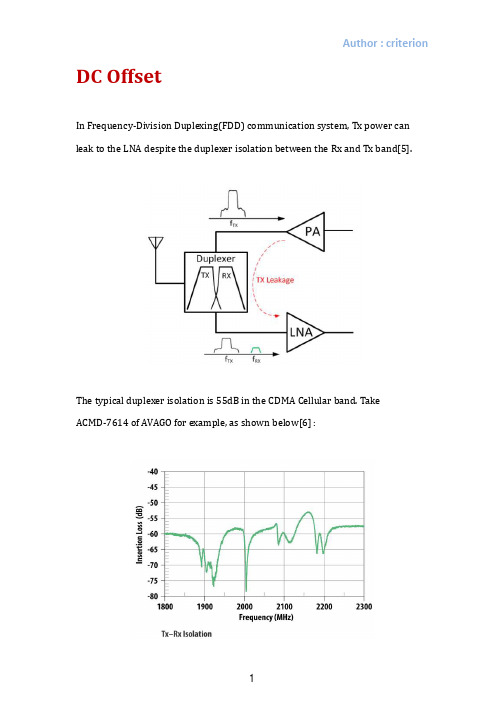
DC OffsetIn Frequency-Division Duplexing(FDD) communication system, Tx power can leak to the LNA despite the duplexer isolation between the Rx and Tx band[5].The typical duplexer isolation is 55dB in the CDMA Cellular band. Take ACMD-7614 of AVAGO for example, as shown below[6] :And the maximum Tx power can be as high as +27dBm at PA output, resulting in -28dBm of Tx power at the Rx input port. We call the phenomenon that Tx power leaks to the Rx port Tx leakage, which may saturate LNA and cause gain reduction if the linearity of LNA is not high enough[5].According to the cascade noise figure formula[5,11] :less the LNA gain, higher the cascade noise figure and worse sensitivity.Zero-IF RF front-end, i.e. direct-conversion receivers(DCR) are attractive for cellular systems due to lower cost and Bill-of-Material (BOM)[2].As shown in the figure below, DCR, as its name implies, RF signal downconverts to baseband near 0 Hz directly.As illustrated below, DC Offset is one of nonlinear effects as well.Consequently, if Tx leakage saturates LNA, there will be DC offset, which will be directed to the baseband signal processing IC, and may result in measurement error and aggravate sensitivity[2,5].Besides, because mixer input is LNA output, it means that mixer should have higher linearity than LNA. Otherwise, due to nonlinearity of mixer, there is still DC offset, even if LNA is linear.IIP2Intermodulation(IMD) is one of nonlinear effects as well. If there are two tones, f1 and f2, with nearly identical frequency, f1 ≈ f2. If the LNA is nonlinear, there will be 2 order IMD (IMD2).IMD2 : f1-f2 ≈ 0 => DC OffsetThat is to say, if the situation occurs, IMD2 is like DC offset and aggravates sensitivity.Similarly, even if LNA is linear, as long as mixer is nonlinear, there will be IMD2 as well.The IMD2 formula is as shown below:= − +C is correction constant. As shown above, we know that higher the input power, higher the IMD2. Because FDD communication system, e.g., CDMA, has Tx leakage. That is to say, Tx power at Rx port dominates IMD2.The CDMA handset receiver needs to handle typically -110 dBm signals when farthest from the base station[13]. In other words, if the equipment is at the cellular boundary, which receives extremely weak signal. Besides, due to the power control, the mobile's transmitter power is kept close to it's maximum level i.e. 23 dBm, to maintain communication quality[14,28].If the situation occurs, the receiver will activate high gain mode to reduce cascade noise figure. As shown below :But, higher the gain, worse the linearity[5]. In this case, in terms of IMD2 formula, input power is maximum, but IIP2 is minimum. Thus, the IMD2 aggravates sensitivity seriously.Because DC Offset and IMD2 are the inherent obstacles of DCR, and difficult to reject without attenuating baseband signal. Thus, some DCRs integrate DC correction and IIP2 calibration circuit.After calibration, the IIP2 improves indeed.And the IMD2 reduces indeed.Besides, by means of DC correction, the IIP2 improves as well.As shown below, more the IIP2, better the sensitivity[1].Because in FDD communication system adopting DCR, the sensitivity is highly dependent on the IIP2 performance[1], that’s the reason why we have to care IMD2 so much. Generally speaking, the CDMA receiver should have 55 dBm IIP2 with high gain mode. For example, the WTR3925 of Qualcomm has exactly 54 dBm IIP2 with high gain mode, and test conditions for the IIP2 measurements: one signal tone and two equal-level CW jammers having levels as stated in the table below[12] :Adjacent Channel SelectivityIn the test specification of the 3GPP standard, the adjacent channel selectivity (ACS) is a measure of the receiver’s ability to receive a wanted signal at its assigned channel frequency in the presence of an strong adjacent channel signal at a given frequency offset from the center frequency of the assigned (wanted) channel, and with acceptable frame error rate(FER) [23].As mentioned above, Intermodulation(IMD) is one of nonlinear effects as well. If there are two tones near wanted signal, f1 and f2, with nearly identical frequency, f1 ≈ f2. If the LNA is nonlinear, there will be 3 order IMD (IMD3).IMD3 : 2f1-f2 or 2f2-f1 ≈ wanted signal.As illustrated below :Because the IMD3 is near wanted signal, which is not able to be filtered. It will interfere the wanted signal.Similarly, even if LNA is linear, as long as mixer is nonlinear, there will be IMD3 as well.In terms of linearity, more the IIP3, better the ACS. The WTR3925 of Qualcomm has about -10 dBm IIP3(ACS) with high gain mode, and test conditions for this IIP3 measurement: one signal tone and two equal-level CW jammers having levels as stated in the table below[12] :Cross ModulationAs mentioned above, as long as two tones pass through a nonlinear device simultaneously, there will be IMD. Besides, if one of the two tones is nonconstant envelope modulated signal, there will be cross modulation(XMD) as well. In other words, with nonconstant envelope modulated signal, the nonlinearity results in not only IMD, but also XMD. Conversely, no nonconstant envelope modulated signal, no XMD[19].In real environment, there are three tones at the CDMA Rx port : Tx signal, Rx signal, and blocker(a.k.a. jammer)[5]In terms of mathematics[18], assuming the LNA input signal x(t), with blocker and TX leakage signal then we get:The former is CW jammer, the latter is Tx signal. And the output signal can be expressed as third order nonlinearity:Substituting x(t) in y(t) and we get :As shown above, the term shows the blocker signal being modulated by the square of the amplitude of the TX leakage. Thus, the TX signal leakage signal is cross-modulated with a strong blocker by the third-order non-linearities in the LNA[13,18]. If the CW jammer is near Rx band, the cross modulated signal, i.e. XMD, falling into the receive channel[24].And the simulated spectrum at the output of the LNA is shown in the figure below[14] :And the measured spectrum at the output of the LNA is shown in the figure below[13] :The green trace shows the wanted signal without the presence of jammer or the Tx signal, and the blue trace shows the noise-rise when the jammer and CDMA Tx signal are turned on.Consequently, with Tx leakage and jammer, the LNA nonlinearity can cause IMD3 and XMD simultaneously[26].As mentioned above, the Tx leakage signal may saturate LNA. Nevertheless,let’s take SKY74092-11 of SKYWORKS for example[17]. It is a LNA for CDMA, and its P1dB is -7 dBm in high gain mode. As mentioned above, more the LNA gain, worse the linearity. That is to say, its worst P1dB is -7 dBm. And as mentioned above, the maximum Tx power can result in -28dBm of Tx power at the Rx input port. In other words, it must have enough linearity to avoid being saturated by Tx leakage signal. TX leakage produces very little desensitization of wanted RX signal[14]. But the time varying envelope of the transmitter leakage signal can cause excessive cross modulation of the strong single tone jammer largely due to the third order nonlinearity of the LNA[14]. The formula is illustratedbelow[18] :C is correction constant. As mentioned above, both IMD3 and XMD are produced due to nonlinearity simultaneously. And as seen from the formula, XMD is larger than IMD3, and as shown below[5] :As mentioned above, the increased transmitter leakage into the receiver is not generally a problem on its own. Only the combination of TX leakage and Jammer produces XMD that can’t be filtered away, and imposes requirement for high LNA IIP3 and duplexer isolation[14]. After all, we note that XMD increases by 2dB as the Tx leakage power increases by 1dB(i.e. duplexer isolation decreases by 1dB), and as the IIP3 decreases by 1dB[7]. Generally speaking, the required LNA IIP3 is approximately 8 dBm with duplexer isolation of 50dB[1, 7]. Take ACMD-7614 of AVAGO and SKY74092-11 of SKYWORKS for example, their isolation and IIP3 are 55 dB and 9 dBm(high gain mode) respectively[17].Therefore, the XMD consideration is shown in the figure below[14] :With constant Tx power, more the isolation, less the XMD[14] :In terms of spectrum, without Tx leakage, the noise floor is obviously lower[7] :Besides, higher the IIP3, less the XMD[7] :In terms of spectrum, higher the IIP3, lower the noise floor[7] :Thus, it forces the use of highly linear LNAs which require very high IP3 at the expense of large current[14, 15].Or by means of linearization to reduce XMD[14] :Single-tone desensitizationIn designing CDMA receiver, one of the stringent requirements is the singletone desensitization(STD) test[7].Single-tone desensitization(STD) performance is a measure of a cell phone receiver’s ability to receive a CDMA signal at its assigned channel frequency in the presence of a nearby narrow-band jammer spaced at a given frequency offset from the center frequency of the assigned channel, and in the presence of Tx leakage signal. The receiver desensitization performance is measured by the FER (≤ 0.5%)[13]. The figure is illustrated as below[14] :When testing a CDMA front-end IC (or a zero-IF receiver) for single-tone desensitization performance, it is important to note the interference components created by the single-tone jammer and recreate the effects in the test setup. There are two main contributors to single-tone desensitization performance: XMD and reciprocal mixing. XMD is as mentioned above, so we discuss reciprocal mixing next[13].In STD test, the strong CW Jammer is near Rx signal. Reciprocal mixing occurs when the single-tone jammer mixes with the receiver’s local oscillator (Rx LO). Rx LO has finite phase noise that mixes with single-tone jammer, and creates an interference component at the baseband, as illustrated in the figure above[13].It can be seen that the receiver single-tone desensitization specification is akey performance parameter that sets the LO phase noise requirement. Thus, without Tx leakage, the reciprocal mixing product can aggravate sensitivity as well.In addition, it is important to note that the single-tone jammer’s own sidelobe also contributes to the overall interference level. That is to say, without Tx leakage and LO phase noise, single-tone jammer’s own sidelobe can aggravate sensitivity as well, as illustrated below[13] :Consequently, for accurate single-tone desensitization measurement, it is necessary to choose a low sidelobe RF signal source so that the main contributor to single-tone desensitization comes from the receiver LO’s phase noise and not the RF signal generator’s sidelobe. The detailed STD test setup is as illustrated below [13]:As analyzed above, we know that STD test becomes the key determiner of the linearity and phase noise requirements of the CDMA receiver[1].Triple BeatTriple beat(TB) test is employed to mimic the XMD distortion scenario and validate the performance in CDMA receiver[4]. Consider three tones at LNA input : f1, f2 and f3.f1 and f2 are at Tx frequency, and f3 is at Rx frequency. There will be TB components :±( − )If f1 and f2 are very close, then the TB components shown above falls in Rx band. The following figure shows the TB component produced due to f1 and f2 along with f3, falling in the vicinity of f3[4].As illustrated above, we define the amplitude between TB components and f3 as triple beat ratio(TBR).In terms of mathematics, consider a nonlinear LNA whose input-output characteristic is represented by a 3rd order polynomial given by[4] :where, Vo(t)is the output voltage of the LNA, and Vi(t)is the input voltage applied to the LNA. Let’s assume Vi(t) has three tones, as shown in the formula below :whereSubstituting Vi(t) in Vo(t) and grouping the same order terms we get :Still according to mathematical analysis[4], we conclude that the highest power TB component is 6dB higher than IMD3 component produced by two tone test. Thus, TB test is also the key determiner of the IIP3. Higher the IIP3, higher the TBR. The WTR3925 of Qualcomm has about -4 dBm IIP3(TB) with high gain mode, and test conditions for this IIP3 measurement: one signal tone, one CW jammer, and two equal-level CW jammers (Tx signals) having levels as stated below[12] :Besides, some engineers are evaluating switches and duplexers to be used in their CDMA transceiver designs, and for suppliers who are verifying the linearity performance of their switches and duplexers. Qualcomm has published two documents[20,21], which describe the TB test procedure.LinearityAs mentioned above, we know that poor linearity leads to poor sensitivity.The receiver cascade IIP3 formula is as below[5] :As seen from the formula, linearity of latter stages becomes increasingly critical. Besides, as mentioned above, mixer input is LNA output, it means that mixer has higher input power than LNA. Thus, mixer has more stringent linearity requirement than LNA. The nonlinearity of the mixer plays a role after the Tx signal is down-converted[1]. An effective solution for improving linearity is using an external SAW filter between LNA and mixer to make the mixer linearity requirement relaxed by attenuating the out of bands blockers[1,5,25, 27].As mentioned above, CDMA has Tx leakage, but Tx rejection by an external SAW filter reduces the mixer linearity(e.g. IIP2 and IIP3) requirement. The SAW filter has about 30 dB Tx rejection, and therefore the mixer is sufficiently protected from XMD. With an external SAW filter , the IIP3 requirement for this mixer is largly determined by the receive band 2-tone interference[14]. Besides, the external SAW filter can be regarded as DC block to reject DC offset or IMD2 due to LNA nonlinearity[22].So, even though the receiver linearity is dominated by the mixer’s linearity, most of the nonlinear distortion occurs in the LNA, as mentioned above.As shown above, that’s the reason why XMD generated by mixer is 30-40dB lower than that of LNA[7].Some LNAs adopt differential architecture to reject even order nonlinearity distortion[1].Because Tx leakage signal at mixer input is very small due to the external SAW filter between the LNA and the mixer[13]. Thus, the external SAW filter after the LNA stage has been an essential component in FDD communication system(e.g. CDMA) adopting DCR architecture [1].Nevertheless, such external SAW filters are expensive and bulky, a SAW–less receiver system is desirable since it eliminates the SAW filter as well as the external matching components[1].But, on the other hand, a SAW-less receiver places an additional linearity burden on the mixer and the following stages. That is to say, in a SAW-less receiver, the mixer becomes the most critical component in terms of the linearity performance of the receiver[1].In order to get low conversion loss from a passive mixer, typically a high LO power is needed, which may result in significant LO leakage due to the finite mixer port to port isolation[2]. LO leakage causes self-mixing, thereby generating a static DC level aggravating sensitivity. As shown below :Although passive mixers have LO leakage issue[2,5]. Nevertheless, compared to active mixers, passive mixers give better linearity performance. The flicker noise (1/f) of the mixer can corrupt the integrated noise, but the passive mixer will not introduce significant flicker noise, since there is no dc current[1]. Consequently, a passive mixer is an essential component in a SAW-less receiver.There have been several efforts to implement a SAW-less CDMA receiver. An embedded filtering passive receiver mixer is used to overcome transmitter power leakage without the use of an external SAW filter, and it has 37dB Txrejection[1].In addition, it also has better low frequency noise(e.g. IMD2) rejection than conventional architecture.The additional rejection provided by embedded filtering passive mixer dramatically improves system linearity performance. It has +65.3dB TBR, which is better than conventional architecture by about 20 dB[1]. And it hasbetter IIP2@45MHz than conventional architecture by about 10 dB.Consequently, as shown above, the proposed embedded filtering passive mixer has better IMD2 rejection than conventional architecture[1].Reference[1] A Highly Linear SAW-less CMOS Receiver Using a Mixer with Embedded TxFiltering for CDMA[2] Introduction to IQ signal, Slideshare[3] Cancellation Techniques for LO Leakage and DC Offset in Direct ConversionSystems[4] Carrier Triple Beat Test[5] Sensitivity or selectivity -- How does eLNA impact the receriver performance,Slideshare[6] ACMD-7614 UMTS Band 1 Duplexer, AVAGO[7] A NIGHTMARE FOR CDMA RF RECEIVER: THE CROSS MODULATION, IEEE[8] Characterization of Cross Modulation in Multichannel Amplifiers Using aStatistically Based Behavioral Modeling Technique, IEEE[9] Presentation on Cross Modulation in a Full Duplex Transceiver, Agilent[10] Cross-modulation in a CDMA Mobile Phone Receiver[11] System(board level) noise figure analysis and optimization, Slideshare[12] WTR39xx Wafer-level RF Transceiver Device Specification, Qualcomm[13] Measuring single-tone desensitization for CDMA receivers[14] Presentation on Cross Modulation in CDMA Mobile Phone Transceivers,KEYSIGHT[15] LNA design for CDMA front end, NXP[16] RF System Design of Transceivers for Wireless Communications[17] Dual-Band LNA for CDMA, Femtocell, and PCS Mobile Handset Applications,SKYWORKS[18] IP2 and IP3 Nonlinearity Specifications for 3G/WCDMA Receivers[19] RF Microelectronics 2nd edition, Razavi[20] Duplexer Linearity Test Procedure, Qualcomm[21] RF Switch Linearity Test Procedure, Qualcomm[22] BGA824N6, Silicon Germanium Low Noise Amplifier for Global NavigationSatellite Systems (GNSS), Infineon[23] Ultra Low Noise Amplifiers Improve Cell Coverage and Reduce Costs[24] Presentation on Cross Modulation in a Full Duplex Transceiver, KEYSIGHT[25] A CDMA2000 Zero-IF Receiver With Low-Leakage Integrated Front-End[26] A Single–Chip 10-Band WCDMA/HSDPA 4-Band GSM/EDGE SAW-less CMOSReceiver With DigRF 3G Interface and 90 dBm IIP2[26] DC Offsets in Direct-Conversion Receivers: Characterization andImplications[27] Circuits and Systems for Future Generations of Wireless Communications[28] Interference Mitigation Techniques for SAW-less CDMA Receivers。
《零中频接收机》课件

研究零中频接收机的线性化技术,降低非线性失真和噪声,提高信 号质量。
高效实现方法
研究零中频接收机的低复杂度实现方法,降低功耗和成本,提高其实 用性。
THANKS
感谢观看
高线性度
由于没有中频滤波器,零中频 接收机能够提供更好的线性度 ,提高了信号的保真度。
低噪声
由于减少了中频电路,零中频 接收机的噪声系数也相应降低 ,提高了信号的信噪比。
易于集成
由于结构简单,零中频接收机 更容易实现小型化和集成化。
挑战
镜像抑制问题
零中频接收机在接收信号时 ,会同时接收到目标信号和 镜像信号,需要采取措施抑 制镜像信号。
特点
结构简单、低功耗、低成本、易 于集成。
工作原理
01
02
03
信号输入
射频信号通过天线接收, 经过低噪放增益放大后进 入混频器。
混频
射频信号与本振信号混频 ,直接下变频到基带信号 。
信号处理
基带信号经过滤波、放大 、解调等处理,最终输出 原始信息。
历史与发展
起源
20世纪90年代,随着微电 子技术的进步,零中频接 收机概念被提出。
解决方案
采用数字滤波器进行镜像抑制
通过数字滤波器对接收到的信号进行处理,抑制镜像信号的影响。
优化本振电路设计
通过优化本振电路的设计,降低本振信号的泄露。
采用开关电源进行电源管理
通过采用开关电源技术,实现高效、稳定的电源管理。
采用校准技术解决通道一致性问题
通过校准技术对接收机的各个通道进行校准,确保通道间的一致性。
05
零中频接收机的未来展望
技术发展趋势
集成化
随着微电子技术的发展,零中频接收机将更加集成化,体积更小 ,功耗更低。
- 1、下载文档前请自行甄别文档内容的完整性,平台不提供额外的编辑、内容补充、找答案等附加服务。
- 2、"仅部分预览"的文档,不可在线预览部分如存在完整性等问题,可反馈申请退款(可完整预览的文档不适用该条件!)。
- 3、如文档侵犯您的权益,请联系客服反馈,我们会尽快为您处理(人工客服工作时间:9:00-18:30)。
WCDMA相较于2G时代的GSM技术,WCDMA在Data Rate与信道容量,都大大提升[1],采用了几个不同于GSM的技术。
一个是CDMA技术,也就是分码多任务,用简单的比喻来比较TDMA, FDMA, CDMA的不同[2] :在会议室内,若要保持通话时不被干扰,一种分别是选择不同时间通话(TDMA)一种是同时间通话,但分别在不同的隔间(FDMA)还有一种是同时间又同隔间通话,但讲不同语言(CDMA)这三种技术,分别在时域跟频域的比较 :由上图可知,CDMA 不分时也不分频,但因为分码,采正交码技术,不同码之间完全没有相关,因此大大提高了安全性。
C另外则是展频技术,将讯号的带宽拓宽,使其带以拓宽,与前述的正交码有送数据没有关系,故的传送数据,因此使得讯号得知,带宽拓宽后,其信道由上式可知,信道容量也跟个位的SNR ,b E 即每个位的式 :便可算出系统的SNR ,使其带宽远大于未作展频调变之原始数据带宽交码有关。
由于Tx 端会采用一组正交码,且该Rx 端也需使用该组正交码,才能解开展频,得讯号不易被干扰与撷取[3],同时也由Shanno 其信道容量也提升了,连带提高了Data Rate[4]量也跟SNR 有关,但在CDMA 中,会先以EN个位的能量,而0N 即噪声的功率频谱密度,其中b f 是Data Rate ,因此若提升0bE N ,则可提升另外,由于原始数据的Chip Rate ,会在展频后大大提升,使得讯号会额外获得增益,进而再提高SNR ,该增益称为处理增益,Processing Gain ,P G()10log()CP R G dB R=R 是原始资料的Chip Rate ,C R 是展频后的Chip Rate ,由[5]可知,R 与C R 分别为12.2Kbps 与3.84Mcps ,带入上式,而得知0bE N 与P G 后,便可算出JM (Jamming Margin) :()10log()10log(bP E JM dB G N =−当然JM 值越大,则表示抗干扰能力越好[3]。
而虽然WCDMA 的Chip Rate 为3.84Mcps ,在频谱上占用3.84MHz 的带宽, 但为了防止相邻频道的干扰,因此上下两端再加入保护频率,所以一个Channel 共占用5MHz 的带宽[6] :至于调变方面,WCDMA 在Downlink ,是采用QPSK 技术,PSK (正交相移键控)是一种调相技术,它规定了四种载波相位,分别为45°,135°,225°,275°。
QPSK 每次调变可传输2个数据位,这些位是通过载波的四种相位来传递的。
解调器会根据星座图及接收到的载波信号的相位来判断发送端发送的数据位[4]。
至于Pulse shaping 方面,shaping ,先简单介绍一下在无线传输过程中,ISI (In 假设有组101101的讯号序尚未传送时,每个Symbol 受到外界干扰,导致Symbo 该现象即ISI ,如下图 :,则是采用RRC (Root -Raised-Cosine)技术[5]一下ISI 。
SI (Inter Symbol Interference)是很难避免的讯号讯号序列,以无线方式传送出去, mbol 都在各自归属的Time slot 内,然而在传送ymbol 的能量会泄漏到其他的Time slot ,影响其虚线为传送讯号,绿色为接收讯号,做一番比较,如下图:可以发现讯号明显失真很多[7]。
引起ISI的原因有许多,其中原因之一,便是来自Group Delay。
由前面可知,传送的讯号,并非真正的方波,原因是真正的方波难以实现,而且会占用过多带宽,因此只好以不影响准位判读,且不会占用太多带宽的梯型来传递讯号。
而由Fourier Transform可知,任何波型都是由众多正弦波组合而成,梯型波形也是,因此当一个梯型波形的众多正弦波,在传递过程中没有同步,该现象即Group Delay,举个简单的譬喻,就好比众多短跑选手,抵达终点的时间纷纷不同,如果都同时抵达,那便是无Group Delay了。
然而上图是Group Delay的时域,若转成频域,可以发现Group delay也会有频率响应,某些频率点的Group delay特别严重。
而当Group Delay过大时,便会引起ISI。
另外在时域图中,蓝色如天桥状的,便是Band Pass Filter,频域图即带宽1GHz的BPF的Group Delay频率响应,因此虽然SAW Filter可以滤除噪声,但也可能会造成Group Delay,进而导致ISI[7-8]。
为了消除ISI,因此在接收端解调前,引入Pulse Shaping的技术,主要功能就是将多余的讯号滤除,留下所需之讯号,方便后续的解调等工作[9],而WCDMA采用的,便是RRC的滤波器。
上图是RRC的时域图,是一个低通滤波器,知名美商Broadcom的商标,即RRC。
而RRC 在时域上的波形,会决定其频域上所占带宽大小,可用下式做说明 :0(1)W W α=+ 01α≤≤W 称之为Nyquist 带宽,而0W 为实际上所占用带宽,α则是Roll-off Factor ,其值大小会决定所占带宽大小,α越小越好,最理想情况是0,即0W 等同于W ,最坏情况是1,即0W 为2倍W ,下图是不同α的时域波形 :对应到频域 :而WCDMA 的α为0.22[15]。
统整前述内容,其WCDMA的特性如下:DCR ( Direct Conversion Receiver )又称Homodyne Receiver,或ZIF (Zero IF) Receiver。
在1932年,法国贝里塞斯(de Bellescize)改善LO的频率稳定度,大幅改良了DCR接收质量。
他比较LO讯号和RF讯号的频率差,修正LO讯号的频率,让LO讯号锁定RF频率。
这个电路是当今锁相回路的起源。
因此,为了解决超外差接收机需要较多组件,导致成本与空间增加的缺点,直接的想法就是将RF讯号降至基频,此称为直接降频接收机,利用高Q值的低通滤波器当通道滤波器,下图即DCR的方块图:然而DCR架构的Sensitivity与Selectivity,却不如超外差架构[13],除此之外,还有其它缺点,像是Self-mixing,even-order nonlinearity……等,下面章节将逐一介绍。
Self Mixing理论上LO端要与LNA以及Mixer有着无限大的隔离度(Isolation),但实际上不可能。
下式为降频混波公式:DCR的RX架构,由于RF信号频率与LO信号频率相同[13,26],因此最后降频待解调的讯号,为直流讯号,会座落在频域上频率点为零之处。
而若LO与LNA以及Mixer的隔离度不够大,会产生LO Leakage,即LO会泄漏至LNA与Mixer的输入端,导致LO与LO混波,称之为Self Mixing,或是由天线辐射出去,对其他接收机造成In-band Blocking Interference[6,10]。
而Self Mixing,会产生直流的噪声,同样也座落在频域上频率点为零之处,因此会干扰待解调的讯号,该现象称之为DC Offset,即整体信号波形位准于示波器上显示时,并不在零轴上,该效应会导致后端阶层之电路饱和,导致RX整体性能劣化。
DC Offset。
而Tx Leakage,也会产生Self Mixing,导致DC Offset[25-26]。
Even Order NonlinearityMixer跟LNA的2阶非线性效应,也会造成讯号失真,若LNA线性度不够,则会有IMD2,座落在直流附近,最后再经过Mixer,另外,因为Mixer处理的讯号,是经过LNA放大后的讯号,因此其P1dB必须比LNA更大,否则即便LNA的线性度够,但若Mixer的线性度不够,一样会有该现象[28]。
其IMD2的带宽,是讯号的两倍:因此便会干扰已降频为直流的讯号,导致解调失败[6,26]上述讨论的皆是两个Tone 输出函数简化至二次项[6]由上式可知,即便没有效应,产生DC Offset ,因此多,故LNA 与Mixer的分析,但如果将输入讯号设为一个IMD ,输入讯号只有单一频率,一样因此,由于相较于超外差接收器,DCR 的滤的线性,便显得很重要[16]。
,且将输出会因2阶的非线性的滤波I/Q Mismatch由[11]可知,若IQ讯号振幅不相等,则称为IQ Amplitude imbalance。
若IQ讯号相位差不为90度,则称为IQ phase imbalance,而多半会将这两种现象,统称为IQ imbalance,或IQ Mismatch。
前述说过,DCR的RX架构,LO信号频率会与RF信号频率相同,而高频的LO,欲产生90度正交的相位差,本就实属不易[6],因此容易有IQ Mismatch[22]。
另外,由[12]可知,差分讯号具有较佳的抗干扰能力,因此IQ讯号多半都会设计成差分形式。
故差分形式的IQ讯号,其相位差如下:而差分讯号需符合等长,间距固定,以及间距不宜过大的要求,但实际Layout 很难完全符合这些需求,因此也容易有IQ Mismatch[11]。
此外,IQ Mismatch也会引起EVM。
若将IQ Amplitude imbalance定义为ε,IQ phase imbalance定义成θ,则EVM 公式如下[6] :另外,IQ Mismatch也会引起Undesired Sideband,其Mismatch程度,会连带影响,Sideband Suppression的效果[11] :由上图可知,当IQ Amplitude imbalance越小,IQ phase imbalance也越小时,其Sideband Suppression的效果就越好。
而EVM除了来自IQ Mismatch,LO leakage与LO的phase noise,也会引起EVM[18]。
Cross Modulation当有其他用户的Tx讯号,被Rx路径接收时,便会形成Jammer[28]。
而Jammer除了会在Rx路径产生Self Mixing,导致DC Offset外,也会跟Tx Leakage形成Cross Modulation。
上图是Cross Modulation示意图,可以看到其实Tx Leakage与Jammer,在频谱上离接收讯号还有一段距离,但是这两者所产生的Cross Modulation,便会干扰接收讯号,使Sensitivity变差[19]。
而Cross Modulation 的强度,可用下式表示:(2+P )23X MOD Tx Leakage Jammer P P IP C −−=−+其中C 是校正常数。