
TBC-EC系列霍尔电流传感器
失调电流漂移
≤±0.005
mA/℃
线性度
≤0.1
%FS
带宽(-3db)
0~200
KHz
响应时间
100A/us
≤1
us
绝缘电压
50HZ,1min
3.0
KV
工作温度
-40~+85
℃
储存温度
-40~+125
℃
结构参数
使用说明
1当待测电流从传感器穿过,即可在输出端测得电流大小。(注意:错误的接线可能导致传感器损坏)
2.可按用户需求定制不同额定输入和输出电流的传感器。
150(±18V,82Ω)
225(±18V,68Ω)
300(±18V,51Ω)
500(±18V,15Ω)
A
匝比
1:1000
1:1500
1:2000
1:2000
次级线圈阻抗
3045Βιβλιοθήκη 5555Ω
额定输出电流
50±0.5%
50±0.5%
50±0.5%
100±0.5%
mA
电源电压
±12~±18
V
失调电流
±0.2
南京中霍传感科技有限公司
TBC-EC系列霍尔电流传感器
TBC-EC系列霍尔电流传感器是应用霍尔效应原理开发的新一代电流传感器,能在电隔离条件下测量直流、交流、脉冲以及各种不规则波形的电流。
电参数
项目
TBC50EC
TBC75EC
TBC100EC
TBC200EC
额定输入电流
50
75
100
200
A
测量电流范围
霍尔电流传感器原理图

霍尔电流传感器原理图模块名称:闭环霍尔电流传感器模块参数:测量频率: 0~100KHz测量范围: 1A~40,000A精度: 0.2%~1%相应时间: <1uS线性度: 0.1%无测量插入损耗测量AC,DC及脉冲电流原边电流与副边输出信号高度隔离模块原理图:工作原理:被测电流In流过导体产生的磁场,由通过霍尔元件输出信号控制的补偿电流Im流过次级线圈产生的磁场补偿,当原边与副边的磁场达到平衡时,其补偿电流Im即可精确反映原边电流In值。
霍尔电流传感器型号说明1、前三个字母表示霍尔效应电流传感器分类:DCH表示开环,直放式霍尔效应电流传感器,输出多为电压(V)。
DBC表示闭环,磁平衡霍尔效应电流传感器,输出多为电流(mA);也有少部分转换成电压(V)输出。
DVC表示闭环,霍尔效应电压传感器,输出形式同上。
DDC表示直流小电流传感器,磁调制原理,输出形式同上。
DZ表示转换器。
2、中间数字表示上述传感器的额定值电流传感器为安培(A),电压传感器为安匝(IT)或最高工作电压(V)。
一、后辍字母表示内孔及安装固定方式矩形窗口(内孔),螺钉固定,插座输出,不加字母。
圆形内孔用O表示,线路板安装用P表示。
单电源用D表示。
可拆卸结构用K表示。
二、特殊说明,用通用技术语言表示。
我公司大规格(2KA以上)霍尔电流传感器与国内外同类产品比较主要特点如下:1、磁路采用去剩磁技术措施,磁失调<0.05%。
一般产品磁失调达百分级,已接触到国外公司产品也不例外。
部分产品由于过载产生剩磁,可使产品报废。
2、本产品对外磁场干扰,采用外磁场抵消法;双路磁路使干扰磁场相对抵消。
而信号磁场设计在强磁场状态,外磁场比信号磁场弱,影响可忽略。
3、电路采用双恒温措施,减少温漂,提高稳定度。
大型电流传感器采用多霍尔对称部局、强信号磁场,大大减轻了霍尔元件的不等位影响。
上述技术措施,本公司大型电流传感具有如下特点:(1)高准确度、高稳定性、高可靠性,可适用任何工作现场。
互感器选型手册
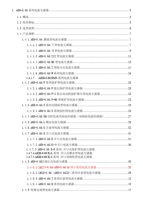
1.1 概述............................................................................................................................................5 1.2 技术指标....................................................................................................................................5 1.3 选型说明....................................................................................................................................6 1.4 产品规格....................................................................................................................................7
1.4.9.1 AKH-L 零序电流互感器.....................................................................................47 1.4.9.2 AKH-3.3/P-φ型中压电动机保护专用电流互感器......................................49 1.4.9.3 JDG4-0.5 电压互感器.......................................................................................49 1.4.9.4 AMZK 系列电流互感器.......................................................................................50 1.5 安装方法...................................................................................................................................51 1.6 附录...........................................................................................................................................55 1.6.1 附录 1............................................................................................................................55 1.6.2 附录 2............................................................................................................................56 1.6.3 附录 3............................................................................................................................57 2. 霍尔传感器.......................................................................................................................................58 2.1 开环霍尔电流传感器..............................................................................................................58 2.2 闭环霍尔电流传感器..............................................................................................................62 2.3 直流漏电流传感器...................................................................................................................63 2.4 直流电压传感器......................................................................................................................65 3.BR 系列罗氏线圈变送器....................................................................................................................67 4.BA 系列交流电流传感器....................................................................................................................69 5.BM 系列模拟信号隔离器....................................................................................................................72 6.BD 系列电力变送器............................................................................................................................76 7. 典型案例...........................................................................................................................................82 8. 获得证书...........................................................................................................................................85
闭环霍尔电流传感器 结构
闭环霍尔电流传感器结构摘要:1.闭环霍尔电流传感器的概念与原理2.闭环霍尔电流传感器的结构3.闭环霍尔电流传感器的工作过程4.闭环霍尔电流传感器的应用领域5.闭环霍尔电流传感器与开环霍尔电流传感器的区别正文:闭环霍尔电流传感器是一种基于霍尔效应原理的电流检测设备,它能够对电路中的电流进行精确测量。
相较于开环霍尔电流传感器,闭环霍尔电流传感器具有更高的精度和线性度。
下面我们将详细介绍闭环霍尔电流传感器的结构、工作过程以及应用领域。
1.闭环霍尔电流传感器的概念与原理闭环霍尔电流传感器利用霍尔效应原理,通过原边电流产生的磁场与副边电流产生的磁场相抵消,使霍尔器件处于检测零磁通的工作状态。
这样,原边电流与副边电流之比等于匝数比的倒数,从而实现对原边电流的精确测量。
2.闭环霍尔电流传感器的结构闭环霍尔电流传感器主要由原边绕组、副边绕组、磁芯和霍尔元件组成。
原边绕组通入被测电流,产生磁场;副边绕组由电子电路产生补偿电流,产生相反的磁场;磁芯用于集中磁场;霍尔元件则用于检测磁通。
3.闭环霍尔电流传感器的工作过程当原边电流通过磁芯时,会产生一个磁场。
这个磁场会穿过副边绕组,并在其中产生一个感应电动势。
通过调整副边绕组的电阻,使得副边产生的补偿电流与原边电流产生的磁场相抵消,从而使磁芯中的磁通为零。
这时,霍尔元件检测到的磁通为零,从而实现对原边电流的精确测量。
4.闭环霍尔电流传感器的应用领域闭环霍尔电流传感器广泛应用于工业自动化、电动汽车、电力设备、交通运输等领域,用于测量电路中的电流,为系统的控制和保护提供精确的数据支持。
5.闭环霍尔电流传感器与开环霍尔电流传感器的区别闭环霍尔电流传感器与开环霍尔电流传感器的主要区别在于结构和原理。
开环霍尔电流传感器的输出正比于霍尔片垂直的磁感应强度,而磁感应强度除了与被测电流相关之外,还与铁芯的磁导率相关,因此其精度较低。
TBC-DS5_霍尔电流传感器

TBC-DS5 多量程闭环型霍尔电流传感器的初、次级之间是绝缘的,可用于测量直流、交流和脉冲电流。
TBC-DS5 series multi-range current sensor is a closed loop device based on the measuring principle of the hall effect and null balance method, with a galvanic isolation between primary and secondary circuit. It provides accurate electronic measurement of DC, AC or pulsed currents.●交流变速驱动器AC variable speed drives●直流电机驱动静态转换器Static converters for DC motor drives ●通讯电源Battery supplied applications●不间断电源UPSUninterruptible Power Supplies (UPS) ●开关电源Switched Mode Power Supplies (SMPS)1.当待测电流从传感器穿过,即可在输出端测得电压大小。
(注意:错误的接线可能导致传感器损坏)When the current will be measured goes through a sensor, the voltage will be measured at the output end.(Note: The false wiring may result in the damage of the sensor)2.可按用户需求定制不同额定输入电流和输出电压的传感器。
Custom design in the different rated input current and the output voltage are available.●UL94-V0.●EN60947-1:2004●IEC60950-1:2001●EN50178:1998●SJ 20790-2000脉冲电流信号响应特性抗脉冲电压干扰特性Pulse current signal response characteristic Effects of impulse noise输入信号( Input signal )输出信号( Output signal )输出电压IN213456OUT。
CrossChip Microsystems CC6904 单芯片霍尔效应电流传感器说明书

CC6904单芯片霍尔效应电流传感器5A/10A/20A/30A 系列概述CC6904是一款高性能单端输出的线性电流传感器,可以更为有效的为交流(AC )或者直流(DC )电流检测方案,广泛应用于工业,消费类及通信类设备。
CC6904内部集成了一颗高精度,低噪声的线性霍尔电路和一根低阻抗的主电流导线。
当采样电流流经主电流导线,其产生的磁场在霍尔电路上感应出相应的电信号,经过信号处理电路输出电压信号,使得产品更易于使用。
线性霍尔电路采用先进的BiCMOS 制程生产,包含了高灵敏度霍尔传感器,霍尔信号预放大器,高精度的霍尔温度补偿单元,振荡器,动态失调消除电路和放大器输出模块。
在无磁场的情况下,静态输出为50%VCC 。
在电源电压3.3V 条件下,OUT 可以在0.2~3.1V 之间随磁场线性变化,线性度可达0.4%。
CC6904内部集成的动态失调消除电路使IC 的灵敏度不受外界压力和IC 封装应力的影响。
CC6904提供SOP8封装,工作温度范围-40~125°C 。
特性◆静态共模输出点为50%VCC ◆测量范围宽,5A/10A/20A/30A◆1MHz 斩波频率,高带宽,低噪声,单端模拟输出◆导线引脚到信号引脚有2000V 的安全隔离电压◆低功耗◆常温误差1%,全温误差3%◆温度稳定性好,内部采用了芯进专利的霍尔信号放大电路和温度补偿电路◆抗干扰能力强◆抗机械应力,磁参数不会因为受外界压力而偏移◆ESD (HBM)6000V应用◆电机控制◆负载监测系统◆开关电源◆过流故障保护功能框图订购信息产品名称灵敏度(CC6904SO-05A CC6904SO-10A CC6904SO-20A管脚定义12345678IP+IP+IP-IP-VCC OUT NCGNDSOP8封装极限参数推荐工作环境参数电源电压环境温度直流电流容量参数符号电气特性零电流输出温度系数ΔV OUT(Q)灵敏度温度系数ΔSens典型应用电路典型应用过流故障检测器电流峰值监测应用曲线&波形(若无特别指明,V CC =3.3V @25°C)V OUT vs.IP (正向电流上升沿响应)(20A )V OUT vs.IP (正向电流下降沿响应)(20A )V OUT vs.IP (负向电流上升沿响应)(20A )V OUT vs.IP (负向电流下降沿沿响应)(20A )CH2:OUT CH4:IPCH2:OUT CH4:IPCH2:OUT CH4:IPCH2:OUT CH4:IPt D 响应时间(20A )静态电流vs.VCC 静态电流vs.Ta20A 系列V OUT(Q)vs.Ta(20A)V OUT vs.IP (20A)CH2:OUT CH4:IP468V OUT error vs.Ta(20A)Sens error vs.Ta(20A)封装信息SOP8封装注意:1.所有尺寸单位均为毫米。
霍尔电流传感器测试要求

霍尔电流传感器 AHKC-EKB检测案例
安科瑞电气测试中心对霍尔电流传感器产品按照表1所列的标准进行整机试验一:下面是我中心的测试参照规范:
表1 测试依据
二:检测项目表
检测项目表2
三:按照企业标准中的试验等级及国家标准中的试验要求和试验方法对产品进行测试,结合本测试中心现有开展项目进行。
期间出现的产品性能异常均及时反馈并及时进行整改,提高了产品的可靠性能,为新产品定型做好了充分的准备。
通过上述我们可以得到,产品在本中心进行相关测试时,检测项目能够按照较全面的覆盖产品的国家标准所要求的检测项目,提前改进,提高产品的质量,降低企业费用。
作者简介:
高杨(1990-),女,本科,就职于江苏安科瑞电器制造有限公司测试中心,致力于于气候环境试验、机械环境试验、材料的阻燃耐热试验等试验研究。
手机:188******** QQ:2881068601。
闭环霍尔电流传感器的工作原理介绍
霍尔电流传感器原理图模块名称:闭环霍尔电流传感器模块参数:测量频率: 0~100KHz测量范围: 1A~40,000A精度: 0.2%~1%相应时间: <1uS线性度: 0.1%无测量插入损耗测量AC,DC及脉冲电流原边电流与副边输出信号高度隔离模块原理图:工作原理:被测电流In流过导体产生的磁场,由通过霍尔元件输出信号控制的补偿电流Im流过次级线圈产生的磁场补偿,当原边与副边的磁场达到平衡时,其补偿电流Im即可精确反映原边电流In值。
闭环霍尔电流传感器的工作原理介绍闭环霍尔电流传感器是利用霍尔器件为核心敏感元件用于隔离检测电流的模块化产品,它的工作原理是霍尔磁平衡式的。
当电流流过一根长的直导线时,在导线周围产生磁场,磁场的大小与流过导线的电流大小成正比,这一磁场可以通过软磁材料来聚集,然后用霍尔器件进行检测,由于磁场的变化与霍尔器件的输出电压信号有良好的线形关系,因此可利用霍尔器件的测得的输出信号,直接反应出导线中的电流大小:I ∝ B ∝ VH (2)式中:B为导线通电流后产生的磁感应强度;I为通过导线中的电流;VH为霍尔器件在磁场B中产生的霍尔电压。
当选择适当的比例系数,上述关系可以表示为等式。
对于霍尔输出电压信号VH的处理,人们设计了许多种电路,但总体来讲可分为两类,一类为开环霍尔电流传感器;另一类为闭环霍尔电流传感器。
闭环霍尔电流传感器的工作原理是磁平衡式的,即原边电流(IN)所产生的磁场,通过一个副边线圈的电流(IM)所产生的磁场进行补偿,使霍尔器件始终处于检测零磁通的工作状态。
当原副边补偿电流产生的磁场在磁芯中达到平衡时:N×IN= n×IM (3)式中:N为原边线圈的匝数;IN为原边电流;n为副边线圈的匝数;IM为副边补偿电流。
由上式看出,当已知传感器原边和副边线圈匝数时,通过测量副边补偿电流IM的大小,即可推算出原边电流IN的值,从而实现了原边电流的隔离测量。
宇波模块
电源 技术领 域应用
宇波模块 宇波模块 宇波模块
负载
AC输入
DC DC
AC电流测量 AC电压测量
整流
PMW转换
整流
DC电流测量 DC电压测量
典型应用:
-通信电源系统 -UPS电源 -铁路信号电源系统 -电力输变电监测系统 -激光电源系统 -工业控制系统电源 -高频加热电源 2006年底,我国合肥建成并投入试运 行的核聚变装置-全超导托卡马克EAST系 统,43台CHB-KA型3KA~20KA霍尔电流传感 器被应用于该装置的供电控制系统,监测 控制供给核聚变装置的能量。 托卡马克EAST装置是为了研究并有效 控制“氢弹爆炸”过程的核聚变反应实验 系统,科学家称其为“人造太阳”,因为 它可以像太阳一样,为人类提供无限、清 洁和安全的能源。
9 13-17
产品认证
宇波模块的设计、生产及 服务 过程通过ISO9001:2000 国际质量管理体系认证。
5A~3000A(AC) 50A~3000A(DC) 1A~300A(AC) 1A~300A(DC)
13 13 17 17 15-16
产品的质量保证
宇波模块 将严格按照ISO9001:2000国际 质量 认证标准 进行设计、生产及服务。我们承诺对由于设计、原材料 及生产工艺造成的产品早期失效负责,产品提供自购买 日期起5年的质量保证。
工作原理:
霍尔磁补偿原理—被测电流IN 流过导体产生的磁场,由通过霍尔元件 输 出信号控制的补偿电流IM 流过次级线圈产生的磁场补偿,当原边与副边 的磁场达到平衡时,其补偿电流IM即可精确反映原边电流IN值。
CHB-50SF CHB-50TF CHB-100A CHB-100P CHB-100S CHB-100T CHB-100SE CHB-100SF CHB-100TF
霍尔TBC-25-50C04
初级引脚 连 接
22
1
4
- + O
注意: 初级安装孔为Φ 次级安装孔为Φ
, 。
接线图 初 1 2 3 4
级
初级接法 IPN(A) 25, 50 12, 25 8, 6, 16 12
峰值电流 IP(A) 55, 100 27, 50 18, 33 13, 25
Байду номын сангаас
输出电流 Is(mA) 25, 50 24, 50 24, 48 24, 48
KEN
R
南京托肯电子科技有限公司 TBC25C04/TBC50C04 型霍尔电流传感器
TBC25C04/TBC50C04 型电流传感器的初、次级之间是绝缘的,可用于测量直流、交流和脉冲电流. 电参数 TBC25C04 25 0~±55 54~360(±15V) 25±0.5% ±15±5% 1-2-3-4:1000 ±0.15 ±0.5 <1 ≤0.1 5 >50 DC…200 40 -40~+85 -40~+125 TBC50C04 50 0~±100 68~180(±15V) 50±0.5% ±15±5% 1-2-3-4:1000 ±0.15 ±0.5 <1 ≤0.1 5 >50 DC…200 30 -40~+85 -40~+125
额定输入有效值电流 测量电流范围 负载阻抗 (额定电流时) 次级额定有效值电流 电源电压 匝 比 零电流失调 电流失调温漂 -40℃~+85℃ 响应时间 线性度 绝缘电压 50(60)HZ,1min di/dt 跟随精度 带宽(-3dB) 次级线圈内阻 @70℃ 工作温度 储存温度 结构参数
A A Ω mA V mA mA µs %FS KV A/μ s KHz Ω ℃ ℃
爱乐高ACS706ELC-05C双向1.5mΩ霍尔效应线性电流传感器IC电路使用手册说明书
NOTE: For detailed information on purchasing options, contact your local Allegro field applications engineer or sales representative.Allegro MicroSystems, Inc. reserves the right to make, from time to time, revisions to the anticipated product life cycle plan for a product to accommodate changes in production capabilities, alternative product availabilities, or market demand. The information included herein is believed to be accurate and reliable. However, Allegro MicroSystems, Inc. assumes no respon-sibility for its use; nor for any infringements of patents or other rights of third parties which may result from its use.Recommended Substitutions:For existing customer transition, and for new customers or new appli-cations, refer to the ACS712.Bidirectional 1.5 mΩ Hall Effect Based Linear Current Sensor ICwith V oltage Isolation and 15 A Dynamic RangeACS706ELC-05CDate of status change: December 26, 2006These parts are in production but have been determined to beNOT FOR NEW DESIGN. This classification indicates that sale of this device is currently restricted to existing customer applications. The device should not be purchased for new design applications because obsolescence in the near future is probable. Samples are no longer available.Not for New DesignFeatures and Benefits• Small footprint, low-profile SOIC8 package• 1.5 m Ω internal conductor resistance• 1600 V RMS minimum isolation voltage between pins 1-4 and 5-8• 4.5 to 5.5 V, single supply operation • 50 kHz bandwidth• 133 mV/A output sensitivity and 15 A dynamic range • Output voltage proportional to ac and dc currents • Factory-trimmed for accuracy• Extremely stable output offset voltage • Near-zero magnetic hysteresis• Ratiometric output from supply voltageThe Allegro ACS706 family of current sensor ICs provides economical and precise solutions for current sensing in industrial, automotive, commercial, and communications systems. The device package allows for easy implementation by the customer. Typical applications include motor control, load detection and management, switch-mode power supplies, and overcurrent fault protection.The device consists of a precision, low-offset linear Hall circuit with a copper conduction path located near the surface of the die. Applied current flowing through this copper conduction path generates a magnetic field which the Hall IC converts into a proportional voltage. Device accuracy is optimized through the close proximity of the magnetic signal to the Hall transducer. A precise, proportional voltage is provided by the low-offset, chopper-stabilized BiCMOS Hall IC, which is programmed for accuracy at the factory.The output of the device has a positive slope (>V CC / 2) when an increasing current flows through the primary copper conduction path (from pins 1 and 2, to pins 3 and 4), which is the path used for current sampling. The internal resistance of this conductive path is typically 1.5 m Ω, providing low power loss. The thickness of the copper conductor allows survival of the device at up to 5× overcurrent conditions. The terminals of the conductive path are electrically isolated from the signal leads (pins 5 through 8). This allows the ACS706 to be used in applications requiring electrical isolation without the use of opto-isolators or other costly isolation techniques.The ACS706 is provided in a small, surface mount SOIC8 package. The leadframe is plated with 100% matte tin, which is compatible with standard lead (Pb) free printed circuit board assembly processes. Internally, the flip-chip uses high-temperature Pb-based solder balls, currently exempt from RoHS. The device is fully calibrated prior to shipment from the factory.Use the following complete part number when ordering:Part NumberPackageACS706ELC-05CSOIC8 surface mountTÜV AmericaCertificate Number:U8V 04 12 54214 005AB S O L UTE MAX I M UM RAT I NGSSupply V oltage, V CC ..........................................16 V Reverse Supply V oltage, V RCC ........................–16 V Output V oltage, V OUT ........................................16 V Reverse Output V oltage, V ROUT ......................–0.1 V Output Current Source, I OUT(Source) ................. 3 mA Output Current Sink, I OUT(Sink) .......................10 mA Maximum Transient Sensed Current *, I R(max) ...100 A Operating Temperature, Maximum Junction, T J(max).......................165°C Storage Temperature, T S ......................–65 to 170°C*Junction Temperature, T J < TJ(max).*100 total pulses, 250 ms duration each, applied at a rate of1 pulse every 100 seconds.Nominal Operating Temperature, T A Range E ............................................–40 to 85ºC Overcurrent Transient Tolerance*, I P ................60 ABidirectional 1.5 m Ω Hall Effect Based Linear Current Sensorwith Voltage Isolation and 15 A Dynamic RangePackage LCPin 1: IP+Pin 2: IP+Pin 3: IP–Pin 4: IP–Pin 8: VCC Pin 7: VOUTPin 6: N.C.Pin 5: GNDPins 6 and 7 are internally connected in shipping product. For compatibility with future devices, leave pin 6 floating.Functional Block Diagram0.1 μFPERFORMANCE CHARACTERISTICS, over operating ambient temperature range, unless otherwise specifiedPropagation Time t PROP I P =±5 A, T A = 25°C– 3.15–μs Response Time t RESPONSE I P =±5 A, T A = 25°C–6–μs Rise Time t r I P =±5 A, T A = 25°C–7.45–μs Frequency Bandwidth f–3 dB, T A = 25°C; I P is 10 A peak-to-peak; no external filter–50–kHzSensitivity Sens Over full range of I P , I P applied for 5 ms; T A = 25°C–133–mV/A Over full range of I P , I P applied for 5 ms124–142mV/ANoise V NOISE Peak-to-peak, T A = 25°C, no external filter–90–mV Root Mean Square, T A = 25°C, no external filter–16–mVLinearity E LIN Over full range of I P , I P applied for 5 ms–±1±4.7% Symmetry E SYM Over full range of I P , I P applied for 5 ms98100104.5% Zero Current Output Voltage V OUT(Q)I P = 0 A, T A = 25°C–V CC / 2–VElectrical Offset Voltage V OE I P = 0 A, T A = 25°C–15–15mV I P = 0 A–65–65mVMagnetic Offset Error I ERROM I P = 0 A, after excursion of 5 A–±0.01±0.05ATotal Output Error1E TOT I P =±5 A, I P applied for 5 ms;T A = 25°C–±1.5–% I P = ±5 A, I P applied for 5 ms––±12.5%Characteristic Symbol Test Conditions Min.Typ.Max.Units ELECTRICAL CHARACTERISTICS, over operating ambient temperature range unless otherwise specifiedOptimized Accuracy Range I P–5–5A Linear Sensing Range I R–15–15A Supply Voltage V CC 4.5 5.0 5.5V Supply Current I CC V CC = 5.0 V, output open5810mA Output Resistance R OUT I OUT = 1.2 mA–12ΩOutput Capacitance Load C LOAD VOUT to GND––10nF Output Resistive Load R LOAD VOUT to GND 4.7––kΩPrimary Conductor Resistance R PRIMARY T A = 25°C– 1.5–mΩRMS Isolation Voltage V ISORMS Pins 1-4 and 5-8; 60 Hz, 1 minute16002500–V DC Isolation Voltage V ISODC–5000–V OPERATING CHARACTERISTICSTHERMAL CHARACTERISTICS2,3, T A = –40°C to 125°C, V CC = 5 V unless otherwise specified–Value–UnitsJunction-to-Lead Thermal Resistance RθJLMounted on the Allegro ASEK 70x evaluation board; additionalinformation about reference boards and tests is available on theAllegro Web site–5–°C/WJunction-to-Ambient Thermal Resistance RθJAMounted on the Allegro ASEK 70x evaluation board; additionalinformation about reference boards and tests is available on theAllegro Web site–41–°C/W1Percentage of I P, with I P = 5 A. Output filtered. Up to a 2.0% shift in E TOT may be observed at end-of-life for this device.2 The Allegro evaluation board has 1500 mm2 of 2 oz. copper on each side, connected to pins 1 and 2, and to pins3 and 4, with thermal vias connect-ing the layers. Performance values include the power consumed by the PWB. Further details on the board are available from the ACS704 Frequently Asked Questions document on our website. Further information about board design and thermal performance also can be found on pages 16 and 17 of this datasheet.3RθJA values shown in this table are typical values, measured on the Allegro evaluation board. The actual thermal performance depends on the board design, the airflow in the system, and thermal interactions between the device and surrounding components through the PCB and the ambient air. To improve thermal performance, see our applications material on the Allegro Web site.Typical Performance Characteristics-50-25255075100125150Supply Current versus Ambient TemperatureV CC = 5 VT A (°C)I C C (m A )4.54.64.74.84.95 5.15.25.35.45.5V CC (V)I C C (m A )8.008.058.108.158.208.258.308.358.408.458.50Supply Current versus Applied VCC11.01.52.02.53.03.54.0-9-8-7-6-5-4-3-2-10123456789V O U T (V )Output Voltage versus Primary CurrentV CC = 5 VI P (A)110115120125130135140145150160S e n s (m V /A )-9-8-7-6-5-4-3-2-1123456789I P (A)Sensitivity versus Primary CurrentV CC = 5 V-50-250255075100125150V O U T (Q ) (V )2.4702.5802.4902.5002.5102.5202.530Zero Current Output Voltage vs. Ambient TemperatureT A (°C)I P = 0 AZero Current Output Currrent versus Ambient Temperature(Data in above chart converted to amperes)I V O U T (Q ) (A )–0.3–0.2–0.10.10.20.3–50–25255075100125150T A (°C)V O M (m A )-1.0-0.8-0.6-0.4-0.200.20.40.60.81.0-50-25255075150100125T A (°C)Magnetic Offset Error versus Ambient TemperatureV CC = 5 V; I P= 0 A, after excursion to 5 A-50-25255075150100125T A (°C)00.51.01.52.02.53.0E L I N (%)Nonlinearity versus Ambient TemperatureV CC = 5 V I P= 5 ATypical Peak-to-Peak Noise of ACS706ELC-05C at T A =25°CStep Response of ACS706ELC-05C at T A =25°CACS706 Output (mV)5 A Excitation SignalTime = 10 μs/div.Excitation signal = 1.00 A/div.Output = 100 mV/div.Time = 20 μs/div.Noise = 20.0 mV/div.ACS706ELC-05C Noise Filtering and Frequency Response Performance Break Frequencyof Filter on Output(kHz)Resistance,R F (kΩ)Capacitance,C F (μF)NominalProgrammedSensitivity(mV/A)FilteredPeak-to-Peak Noise(mV)Resolutionwith Filtering(A)Rise Timefor 5A Step,Filtered(μs)Unfiltered––133 900.6777.45800.2000.01 75.90.5718.26500.32064.70.48610.08 400.39260.30.45311.39 200.80043.30.32617.56 10 1.628.90.21831.96 7.0 3.1518.30.13754.55 3.3 4.813.80.10481.77 0.626 1.90.015404.16 0.3530.760.00573732.89OUTTypical Application DrawingThe ACS706 outputs an analog signal, V Sig. that varies linearly with the bidirectional primarysensed current, I P, within the range specified. R F and C F, are recommended for noise management,with values that depend on the application, as shown in the noise filtering table.Sensitivity (Sens). The change in device output in response to a 1 A change through the primary conductor. The sensitivity is the prod-uct of the magnetic circuit sensitivity (G / A ) and the linear IC amplifier gain (mV/G). The linear IC amplifier gain is programmed at the factory to optimize the sensitivity (mV/A) for the full-scale current of the device.Noise (V NOISE ). The product of the linear IC amplifier gain (mV/G) and the noise floor for the Allegro Hall effect linear IC (≈1 G). The noise floor is derived from the thermal and shot noise observed in Hall elements. Dividing the noise (mV) by the sensitivity (mV/A) provides the smallest current that the device is able to resolve.Linearity (E LIN ): The degree to which the voltage output from the device varies in direct proportion to the primary current through its full-scale amplitude. Nonlinearity in the output can be attributed to the saturation of the flux concentrator approaching the full-scale current. The following equation is used to derive the linearity:Definitions of Accuracy Characteristics1001– [{[{V out_full-scale amperes –V OUT(Q)()2 (V out_half-scale amperes –V OUT(Q))100where V out_full-scale amperes = the output voltage (V) when the sensed current approximates full-scale ±I P .Symmetry (E SYM ). The degree to which the absolute voltage output from the device varies in proportion to either a positive or nega-tive full-scale primary current. The following formula is used to derive symmetry:Quiescent output voltage (V OUT(Q)). The output of the device when the primary current is zero. For a unipolar supply voltage, it nominally remains at V CC ⁄ 2. Thus, V CC = 5 V translates into V OUT(Q) = 2.5 V . Variation in V OUT(Q) can be attributed to the resolution of the Allegro linear IC quiescent voltage trim and thermal drift.Electrical offset voltage (V OE ). The deviation of the device output from its ideal quiescent value of V CC / 2 due to nonmagnetic causes. To convert this voltage to amperes, divide by the device sensitivity, Sens.Accuracy (E TOT ). The accuracy represents the maximum deviation of the actual output from its ideal value. This is also known as the total ouput error. The accuracy is illustrated graphically in the Output V oltage versus Current chart on the following page.Accuracy is divided into four areas:∙ 0 A at 25°C. Accuracy at zero current flow at 25°C, without the effects of temperature.∙ 0 A over Δ temperature. Accuracy at zero current flow including temperature effects.∙ Full-scale current at 25°C. Accuracy at the full-scale current at 25°C, without the effects of temperature.∙ Full-scale current over Δ temperature. Accuracy at full-scale current flow including temperature effects.Ratiometry . The ratiometric feature means that its 0 A output, V OUT(Q), (nominally equal to V CC /2) and sensitivity, Sens, are propor-tional to its supply voltage, V CC . The following formula is used to derive the ratiometric change in 0 A output voltage, ∆V OUT(Q)RAT (%):100V IOUT(Q)VCC /V IOUT(Q)5VV CC /5 VThe ratiometric change in sensitivity, ∆Sens RAT (%), is defined as:100Sens VCC /Sens 5V V CC /5 V ‰Output voltage vs. current, illustrating device accuracy at 0 A and at full-scale currentDefinitions of Dynamic Response CharacteristicsPropagation delay (t PROP): The time required for the device output to reflect a change in the primary cur-rent signal. Propagation delay is attributed to inductive loading within the linear IC package, as well as in the inductive loop formed by the primary conductor geometry. Propagation delay can be considered as a fixed time offset and may be compensated.Response time (t RESPONSE): The time interval between a) when the primary current signal reaches 90% of its final value, and b) when the device reaches 90% of its output corresponding to the applied current.Rise time (t r): The time interval between a) when the device reaches 10% of its full scale value, and b) when it reaches 90% of its full scale value. The rise time to a step response is used to derive the bandwidth of the device, in which ƒ(–3 dB) = 0.35 / t r. Both t r and t RESPONSE are detrimentally affected by eddy current losses observed in the conductive IC ground plane.Device Branding Key (Two alternative styles are used)ACS706T ELC05C YYWWA ACS Allegro Current Sensor706Device family numberT Indicator of 100% matte tin leadframe platingE Operating ambient temperature range codeLC Package type designator05C Primary sensed currentYY Manufacturing date code: Calendar year (last two digits) WW Manufacturing date code: Calendar weekA Manufacturing date code: Shift codeACS706T ELC05CL...L YYWWACS Allegro Current Sensor706Device family numberT Indicator of 100% matte tin leadframe platingE Operating ambient temperature range codeLC Package type designator05C Primary sensed currentL...L Manufacturing lot codeYY Manufacturing date code: Calendar year (last two digits)WW Manufacturing date code: Calendar week Standards and Physical SpecificationsParameter SpecificationFlammability (package molding compound)UL recognized to UL 94V-0Fire and Electric Shock UL60950-1:2003EN60950-1:2001CAN/CSA C22.2 No. 60950-1:2003Chopper Stabilization TechniqueChopper Stabilization is an innovative circuit technique that is used to minimize the offset voltage of a Hall element and an associated on-chip amplifier. Allegro patented a Chopper Stabilization technique that nearly eliminates Hall IC output drift induced by temperature or package stress effects. This offset reduction technique is based on a signal modulation-demodulation process. Modulation is used to separate the undesired dc offset signal from the magnetically induced signal in the frequency domain. Then, using a low-pass filter, the modu-lated dc offset is suppressed while the magnetically induced signal passes through the filter. As a result of this chopper stabilization approach, the output voltage from the Hall IC is desensitized to the effects of temperature and mechanical stress. This technique produces devices that have an extremely stable Electrical Offset V oltage, are immune to thermal stress, and have precise recoverability after temperature cycling.This technique is made possible through the use of a BiCMOS process that allows the use of low-offset and low-noise amplifiers in combination with high-density logic integration and sample and hold circuits.Concept of Chopper Stabilization TechniqueApplications InformationIn order to quantify transient common-mode voltage rejection for the ACS706, a device was soldered onto a printedcircuit board. A 0.1 μF bypass capacitor and a 5 V dc power supply were connected between VCC and GND (pins 8 and5) for this device. A 10 k Ω load resistor and a 0.01 μF capacitor were connected in parallel between the VOUT pin andthe GND pin of the device (pins 7 and 5).A function generator was connected between the primary current conductor (pins 1 thru 4) and the GND pin ofthe device (pin 5). This function generator was configured to generate a 10 V peak (20 V peak-to-peak) sinewave between pins 1-4 and pin 5. Note that the sinusoidal stimulus was applied such that no electrical currentwould flow through the copper conductor composed of pins 1-4 of this device.The frequency of this sine wave was varied from 60 Hz to 5 MHz in discrete steps. At each frequency, thestatistics feature of an oscilloscope was used to measure the voltage variations (noise) on the ACS706 outputin mV (peak to peak). The noise was measured both before and after the application of the stimulus. Transientcommon-mode voltage rejection as a function of frequency is shown in the following figure.Transient Common-Mode Voltage Rejection in the ACS706(kHz)Frequency of 20 V Peak-to-Peak Stimulus –60–55–50–45–40–35–30Tr a nsi e ntR ej ect i o n(d B)The Effect of PCB Layout on ACS706 Thermal PerformanceEight different PC boards were fabricated to characterize the effect of PCB design on the operating junction temperature of the Hall-effect IC inside of the ACS706. These PC boards are shown in the figure below. 2 oz. Cu on one side of board 2 oz. Cu on both sides of board An ACS706 device was soldered on to each PCB for thermal testing. The results of the testing are shown in the following table.Test Results on Eight Thermal Characterization PCBsTested at 15A, T A = 20°C, still air, 2 oz. copper traces, current carried on and off boardby 14 gauge wiresPC BoardsSides with Traces Trace Width (mm)Trace Length (mm)Temperature Rise Above Ambient (°C)1 450901.550Overheated 410481.5101102450531.550106410381.51054Improved PC Board DesignsThe eight PC boards in the figure above do not represent an ideal PC board for use with the ACS706. The ACS706 evaluation boards, for sale at the Allegro Web site On-Line Store, represent a more optimal PC board design (see photo below). On the evaluation boards, the current to be sensed flows through very wide traces that were fabricated using 2 layers of 2 oz. copper. Thermal management tests were conducted on the Allegro evaluation boards and all tests were performed using the same test conditions described in the bulleted list above. The results for these thermal tests are shown in the table below. When using the Allegro evaluation boards we see that even at an applied current of 20 A the junction temperature of the ACS706 is only ≈30 degrees above ambient temperature.Test Results on Eight Electrical Characterization PCBsTested at T A = 20°C, still airApplied Current(A)Temp Rise Above Ambient( C)1522 2031Allegro Current sensor IC evaluation board with ACS706 and external connections.The products described herein are manufactured under one or more of the following U.S. patents: 5,045,920; 5,264,783; 5,442,283; 5,389,889; 5,581,179; 5,517,112; 5,619,137; 5,621,319; 5,650,719; 5,686,894; 5,694,038; 5,729,130; 5,917,320; and other patents pending.Allegro MicroSystems, Inc. reserves the right to make, from time to time, such de p ar t ures from the detail spec i f i c a t ions as may be required topermit improvements in the per f or m ance, reliability, or manufacturability of its products. Before placing an order, the user is cautioned to verify that the information being relied upon is current.Allegro products are not authorized for use as critical components in life-support devices or sys t ems without express written approval.The in f or m a t ion in c lud e d herein is believed to be ac c u r ate and reliable. How e v e r, Allegro MicroSystems, Inc. assumes no re s pon s i b il i t y for its use; nor for any in f ringe m ent of patents or other rights of third parties which may result from its use.Copyright©2005, 2006 Allegro MicroSystems, Inc.Package LC, 8-pin SOICPreliminary dimensions, for reference onlyDimensions in millimetersU.S. Customary dimensions (in.) in brackets, for reference only(reference JEDEC MS-012 AA)Dimensions exclusive of mold flash, gate burrs, and dambar protrusionsExact case and lead configuration at supplier discretion within limits shownA Terminal #1 mark area。