半导体工艺学silvaco仿真实验报告
Silvaco工艺及器件仿真2

4.1.7栅氧厚度的最优化下面介绍如何使用DECKBUILD中的最优化函数来对栅极氧化厚度进行最优化。
假定所测量的栅氧厚度为100Å,栅极氧化过程中的扩散温度和偏压均需要进行调整。
为了对参数进行最优化,DECKBUILD最优化函数应按如下方法使用:a.依次点击Main control和Optimizer…选项;调用出如图4.15所示的最优化工具。
第一个最优化视窗显示了Setup模式下控制参数的表格。
我们只改变最大误差参数以便能精确地调整栅极氧化厚度为100Å;b.将Maximum Error在criteria一栏中的值从5改为1;c.接下来,我们通过Mode键将Setup模式改为Parameter模式,并定义需要优化参数(图4.16)。
图4.15 DECKBUILD最优化的Setup模式图4.16 Parameter模式需要优化的参数是栅极氧化过程中的温度和偏压。
为了在最优化工具中对其进行最优化,如图4.17所示,在DECKBUILD窗口中选中栅极氧化这一步骤;图4.17 选择栅极氧化步骤d.然后,在Optimizer中,依次点击Edit和Add菜单项。
一个名为Deckbuild:Parameter Define的窗口将会弹出,如图4.18所示,列出了所有可能作为参数的项;图4.18 定义需要优化的参数e.选中temp=<variable>和press=<variable>这两项。
然后,点击Apply。
添加的最优化参数将如图4.19所示一样列出;图4.19 增加的最优化参数f.接下来,通过Mode键将Parameter模式改为Targets模式,并定义优化目标;g.Optimizer利用DECKBUILD中Extract语句的值来定义优化目标。
因此,返回DECKBUILD的文本窗口并选中Extract栅极氧化厚度语句,如图4.20所示;图4.20 选中优化目标h.然后,在Optimizer中,依次点击Edit和Add项。
半导体工艺学silvaco仿真实例——扩散
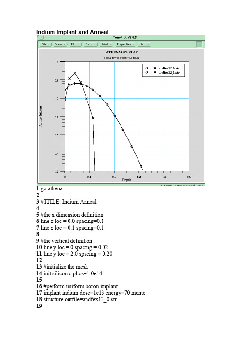
Indium Implant and Anneal1 go athena23 #TITLE: Indium Anneal45 #the x dimension definition6 line x loc = 0.0 spacing=0.17 line x loc = 0.1 spacing=0.189 #the vertical definition10 line y loc = 0 spacing = 0.0211 line y loc = 2.0 spacing = 0.201213 #initialize the mesh14 init silicon c.phos=1.0e141516 #perform uniform boron implant17 implant indium dose=1e13 energy=70 monte18 structure outfile=andfex12_0.str1920 #perform diffusion21 diffuse time=30 temperature=1000222324 extract name="xj" xj silicon mat.occno=1 x.val=0.0 junc.occno=12526 #save the structure27 structure outfile=andfex12_1.str2829 tonyplot -overlay andfex12_0.str andfex12_1.str -set andfex12.set3031 quitOxidation Enhanced Diffusion of Boron1 go athena23 # OED of Boron45 #the x dimension definition6 line x loc = 0.0 spacing=0.17 line x loc = 0.1 spacing=0.189 #the vertical definition10 line y loc = 0 spacing = 0.0211 line y loc = 2.0 spacing = 0.2012 line y loc = 25.0 spacing = 2.51314 #initialize the mesh15 init silicon c.boron=1.0e141617 #perform uniform boron implant18 implant boron dose=1e13 energy=701920 #set diffusion model for OED21 method two.dim2223 #perform diffusion24 diffuse time=30 temperature=1000 dryo225 #26 extract name="xj_two.dim" xj silicon mat.occno=1 x.val=0.0 junc.occno=12728 #save the structure29 structure outfile=andfex02_0.str3031 # repeat the simulation with default FERMI model32 go athena3334 #TITLE: Simple Boron Anneal3536 #the x dimension definition37 line x loc = 0.0 spacing=0.138 line x loc = 0.1 spacing=0.13940 #the vertical definition41 line y loc = 0 spacing = 0.0242 line y loc = 2.0 spacing = 0.2043 line y loc = 25.0 spacing = 2.54445 #initialize the mesh46 init silicon c.phos=1.0e144748 #perform uniform boron implant49 implant boron dose=1e13 energy=705051 #select diffusion model52 method fermi5354 #perform diffusion55 diffuse time=30 temperature=1000 dryo256 #57 extract name="xj_fermi" xj silicon mat.occno=1 x.val=0.0 junc.occno=1585960 #save the structure61 structure outfile=andfex02_1.str6263 # compare diffusion models64 tonyplot -overlay andfex02_0.str andfex02_1.str -set andfex02.set Emitter Push Effect1 go athena23 #TITLE: Emitter push effect example4 #5 line x loc=0.0 spac=0.26 line x loc=2.5 spac=0.87 line x loc=3.0 spac=0.28 #9 line y loc=0.00 spac=0.0410 line y loc=0.3 spac=0.0611 line y loc=2.0 spac=0.812 line y loc=10.0 spac=2.013 #14 init c.phos=1e1515 #16 implant boron dose=1e13 energy=4017 #18 deposit nitride thick=.2 div=419 #20 etch right nitride p1.x=2.521 relax y.min=1.522 #23 implant phosphor dose=1e16 energy=3024 #25 etch nitride all26 #27 method compress full.cpl28 diffuse time=30 temp=100029 #30 structure outfile=andfex07.str31 #32 tonyplot -st andfex07.str -set andfex07.set3334 quitDamage Enhanced Diffusion of ArsenicThis example demonstrates the damage enhanced diffusion effect in a heavy arsenic implant typical of MOS source/drain or bipolar emitter processing.1 go athena23 #the x dimension definition4 line x loc = 0.0 spacing=0.15 line x loc = 0.1 spacing=0.167 #the vertical definition8 line y loc = 0 spacing = 0.0059 line y loc = 2.0 spacing = 0.2010 line y loc = 25.0 spacing = 2.51112 #initialize the mesh13 init silicon c.boron=1.0e171415 #deposit screen oxide16 deposit oxide thickness=0.005 div=21718 #perform arsenic implant with damage19 implant arsenic dose=1.0e15 energy=40 tilt=7 unit.damage dam.factor=0.12021 #set diffusion model for TED22 method full.cpl2324 #perform diffusion25 diffuse time=15/60 temperature=100026 #27 extract name="xj_fullcpl" xj silicon mat.occno=1 x.val=0.0 junc.occno=12829 #save the structure30 structure outfile=andfex03_0.str3132 # repeat the simulation with FERMI model3334 #the x dimension definition35 line x loc = 0.0 spacing=0.136 line x loc = 0.1 spacing=0.13738 #the vertical definition39 line y loc = 0 spacing = 0.00540 line y loc = 2.0 spacing = 0.2041 line y loc = 25.0 spacing = 2.54243 #initialize the mesh44 init silicon c.boron=1.0e174546 #deposit screen oxide47 deposit oxide thickness=0.005 div=24849 #perform arsenic implant with damage50 implant arsenic dose=1.0e15 energy=40 tilt=7 unit.damage dam.factor=0.15152 #set default model53 method fermi5455 #perform diffusion56 diffuse time=15/60 temperature=100057 #58 extract name="xj_fermi" xj silicon mat.occno=1 x.val=0.0 junc.occno=15960 #save the structure61 structure outfile=andfex03_1.str6263 # compare diffusion models64 tonyplot -overlay andfex03_0.str andfex03_1.str -set andfex03.set。
实验报告4(MOSFET工艺器件仿真)
学生实验报告院别课程名称器件仿真与工艺综合设计实验班级实验三MOSFET工艺器件仿真姓名实验时间学号指导教师成绩批改时间报告内容一、实验目的和任务1.理解半导体器件仿真的原理,掌握Silvaco TCAD 工具器件结构描述流程及特性仿真流程;2.理解器件结构参数和工艺参数变化对主要电学特性的影响。
二、实验原理1. MOSEET基本工作原理(以增强型NMOSFET为例):以N沟道MOSEET为例,如图1所示,是MOSFET基木结构图。
在P型半导体衬底上制作两个N+区,其中一个作为源区,另一个作为漏区。
源、漏区之间存在着沟道区,该横向距离就是沟道长度。
在沟道区的表面上作为介质的绝缘栅是由热氧化匸艺生长的二氧化硅层。
在源区、漏区和绝缘栅上的电极是由一层铝淀积,用于引出电极,引出的三个电极分别为源极S、漏极D和栅极G。
并且从MOSEET衬底上引出一个电极B极。
加在四个电极上的电压分别为源极电压Vs、漏极电压V D、栅极电压V G和衬底偏压V B。
图1 MOSFET结构示意图MOSFET在工作时的状态如图2所示。
Vs V D和V B的极性和大小应确保源区与衬底之间的PN结及漏区与衬底之间的PN结处与反偏位置。
可以把源极与衬底连接在一起,并且接地,即Vs=0,电位参考点为源极,则V G、V D可以分别写为(栅源电压)V GS、(漏源电压)V DS。
从MOSFET的漏极流入的电流称为漏极电流ID。
(1)在N沟道MOSFET中,当栅极电压为零时,N+源区和N+漏区被两个背靠背的二极管所隔离。
这时如果在漏极与源极之间加上电压V DS,只会产生PN 结反向电流且电流极其微弱,其余电流均为零。
(2)当栅极电压V GS不为零时,栅极下面会产生一个指向半导体体内的电场。
(3)当V GS增大到等于阈值电压V T的值时,在半导体内的电场作用下,栅极下的P型半导体表面开始发生强反型,因此形成连通N+源区和N+漏区的N型沟道,如图2所示。
Silvaco_TCAD_工艺仿真1解读
Silvaco学习
ATHENA工艺仿真软件
通过MaskViews 的掩模构造说明,工程师可 以有效地分析在每个工艺步骤和最终器件 结构上的掩模版图变动的影响。
与光电平面印刷仿真器和精英淀积和刻蚀
仿真器集成,可以在物理生产流程中进行 实际的分析。
与ATLAS 器件模拟软件无缝集成
07:38
8
Silvaco学习
可仿真的工艺 (Features and Capabilities)
Bake CMP Deposition Development Diffusion Epitaxy
• Etch • Exposure • Imaging • Implantation • Oxidation • Silicidation
采用默认参数,二维初始化仿真: Init two.d
工艺仿真从结构test.str中开始: Init infile=test.str
GaAs衬底,含硒浓度为1015cm-3,晶向[100]: Init gaas c.selenium=1e15 orientation=100
硅衬底,磷掺杂,电阻率为10Ω.cm Init phosphor resistivity=10
定义衬底: material,orientation,c.impurities,resitivity …
初始化仿真: 导入已有的结构,infile… 仿真维度,one.d,two.d … 网格和结构,space.mult,scale,flip.y …
07:38
15
Silvaco学习
初始化的几个例子
07:38
10
Silvaco学习
工艺仿真流程
1、建立仿真网格 2、仿真初始化 3、工艺步骤 4、抽取特性 5、结构操作 6、Tonyplot显示
@湘 silvaco 五个实验程序 和结论

实验二氧化TCAD工艺模拟实验一、实验目的1. 熟悉Silvaco TCAD的仿真模拟环境;2.掌握氧化工艺的关键影响参数,以及如何在TCAD环境下进行氧化工艺模拟;二、实验要求①仔细阅读实验内容,独立编写程序,掌握基本的TCAD使用;②熟悉氧化的基本原理和关键工艺参数;③记录Tonyplot的仿真结果,并进行相关分析。
设计氧化工艺模拟程序,分析气体分压对氧化速度影响。
go athenaline x location=0.0 spac=0.1line x location=1.0 spac=0.1line y location=0.0 spac=0.05line y location=2.0 spac=0.05initialize two.d c.boron=1.0e15diffuse time=60 temp=1000 f.o2=2 press=2 dryo2structure outfile=press2.strextract name="Tox1" thickness oxide mat.occno=1 x.val=0.5tonyplot press2.str#########line x location=0.0 spac=0.1line x location=1.0 spac=0.1line y location=0.0 spac=0.05line y location=2.0 spac=0.05initialize two.d c.boron=1.0e15diffuse time=60 temp=1000 f.o2=2 press=4 dryo2structure outfile=press4.strextract name="Tox2" thickness oxide mat.occno=1 x.val=0.5 tonyplot press4.str##############line x location=0.0 spac=0.1line x location=1.0 spac=0.1line y location=0.0 spac=0.05line y location=2.0 spac=0.05initialize two.d c.boron=1.0e15diffuse time=60 temp=1000 f.o2=2 press=6 dryo2structure outfile=press6.strextract name="Tox3" thickness oxide mat.occno=1 x.val=0.5 tonyplot press6.str########line x location=0.0 spac=0.1line x location=1.0 spac=0.1line y location=0.0 spac=0.05line y location=2.0 spac=0.05initialize two.d c.boron=1.0e15diffuse time=60 temp=1000 f.o2=2 press=8 dryo2structure outfile=press8.strextract name="Tox4" thickness oxide mat.occno=1 x.val=0.5 tonyplot press8.str数据分析:EXTRACT> extract name="Tox1" thickness oxide mat.occno=1 x.val=0.5 Tox1=813.408 angstroms (0.0813408 um) X.val=0.5extract name="Tox2" thickness oxide mat.occno=1 x.val=0.5Tox2=1160.89 angstroms (0.116089 um) X.val=0.5EXTRACT> extract name="Tox3" thickness oxide mat.occno=1 x.val=0.5 Tox3=1466.97 angstroms (0.146697 um) X.val=0.5EXTRACT> extract name="Tox4" thickness oxide mat.occno=1 x.val=0.5Tox4=1739.47 angstroms (0.173947 um) X.val=0.5根据实验数据分析得随着气体分压的加强氧化速度呈上升的趋势。
实验报告2(三极管器件仿真)

学生实验报告如图所示,定义npn晶体管的网络信息x为2.0,y为1.0,该区域块掺杂n型材料浓度为5e15,设置为均匀分布;n型材料浓度为1e18,设置为高斯分布,峰值为1.0;p型材料浓度为1e18,设置为高斯分布,峰值为0.05,结深为0.15;n型材料浓度为5e19,设置为高斯分布,峰值为0,结深为0.05,在x的右边区域0.8处;p型材料浓度为5e19,设置为高斯分布,峰值为0,在x的左边区域0.8处,从而形成了该结构,包括N+区域,P+区域,P区域,N-区域,N区域图一器件结构2、网格调用及设计#调用atlas器件仿真器go atlas#网络mesh初始化Mesh#定义x方向网格信息x.m l=0 spacing=0.15x.m l=0.8 spacing=0.15x.m l=1.0 spacing=0.03x.m l=1.5 spacing=0.12x.m l=2.0 spacing=0.15#定义y方向网格信息y.m l=0.0 spacing=0.006y.m l=0.04 spacing=0.006y.m l=0.06 spacing=0.005y.m l=0.15 spacing=0.02y.m l=0.30 spacing=0.02y.m l=1.0 spacing=0.12#定义区域信息region num=1 silicon#定义电极信息electrode num=1 name=emitter left length=0.8 electrode num=2 name=base right length=0.5 y.max=0 electrode num=3 name=collector bottom#该区域块掺杂n型材料浓度为5e15,设置为均匀分布doping reg=1 uniform n.type conc=5e15# n型材料浓度为1e18,设置为高斯分布,峰值为1.0doping reg=1 gauss n.type conc=1e18 peak=1.0 char=0.2# p型材料浓度为1e18,设置为高斯分布,峰值为0.05,结深为0.15doping reg=1 gauss p.type conc=1e18 peak=0.05 junct=0.15# n型材料浓度为5e19,设置为高斯分布,峰值为0,结深为0.05,在x的右边区域0.8处doping reg=1 gauss n.type conc=5e19 peak=0.0 junct=0.05 x.right=0.8# p型材料浓度为5e19,设置为高斯分布,峰值为0,在x的左边区域0.8处doping reg=1 gauss p.type conc=5e19 peak=0.0 char=0.08 x.left=1.5#set bipolar models#设置BJT仿真所需要用到的物理模型models conmob fldmob consrh auger print#设置接触类型contact name=emitter n.poly surf.rec#求解初始化solve init#保存结构信息文件save outf=bjtex04_0.str#用tonyplot绘图示意结构文件tonyplot bjtex04_0.str -set bjtex04_0.set(二)对比分析表 3-1发射区掺杂浓度不变,改变基区掺杂浓度器件结构与杂质分布图输出曲线浓度(cm-3)1e161e171e181e19表3-2在不同基区掺杂浓度下的参数电流放大系数β浓度(cm3-)最大集电极电流c I(mA)1e16 1.18576 237.1521e17 1.13197 226.3951e18 0.669093 133.8191e19 0.0579857 11.5971实验结论:由表可知,在发射区掺杂浓度不变,改变基区掺杂浓度下,当基区掺杂浓度逐渐增大,最大集电极电流逐渐减小,电流放大系数减小。
实验六 半导体器件仿真实
实验六半导体器件仿真实验姓名:林少明专业:微电子学学号11342047【实验目的】1、理解半导体器件仿真的原理,掌握Silvaco TCAD 工具器件结构描述流程及特性仿真流程;2、理解器件结构参数和工艺参数变化对主要电学特性的影响。
【实验原理】1. MOSFET 基本工作原理(以增强型NMOSFET 为例):图 1 MOSFET 结构图及其夹断特性当外加栅压为0 时,P 区将N+源漏区隔开,相当于两个背对背PN 结,即使在源漏之间加上一定电压,也只有微小的反向电流,可忽略不计。
当栅极加有正向电压时,P 型区表面将出现耗尽层,随着V GS的增加,半导体表面会由耗尽层转为反型。
当V GS>V T时,表面就会形成N 型反型沟道。
这时,在漏源电压V DS的作用下,沟道中将会有漏源电流通过。
当V DS一定时,V GS越高,沟道越厚,沟道电流则越大。
2. MOSFET 转移特性V DS 恒定时,栅源电压 V GS 和漏源电流 I DS 的关系曲线即是 MOSFET 的转移特性。
对于增强型 NMOSFET ,在一定的 V DS 下, V GS =0 时, I DS =0;只有 V GS >V T 时,才有 I DS >0。
图 2 为增强型 NMOSFET 的转移特性曲线。
图 2 增强型 NMOSFET 的转移特性曲线图中转折点位置处的 V GS (th ) 值为阈值电压。
3. MOSFET 的输出特性对于 NMOS 器件,可以证明漏源电流:令n =oxWC Lμβ,称β为增益因子。
(1)()DS GS T V V V <<-由于 V DS 很小,忽略2DS V 项,可得:I DS 随 V DS 而线性增加,故称为线性区。
(2)()DS GS T V V V <-DS V 增大,但仍小于()GS T V V -,2DS V 项不能忽略。
故:在一定栅源电压下,V DS 越大,沟道越窄,则沟道电阻越大,曲线斜率变小。
Silvaco TCAD 工艺仿真2
Tang shaohua, SCU
E-Mail: shaohuachn@ shaohuachn@
11:23 1 Silvaco学习
上一讲知识回顾
熟悉仿真流程
1、建立仿真网格 2、仿真初始化 3、工艺步骤 4、抽取特性 5、结构操作 6、Tonyplot显示
etch ...
tonyplot
Monte Carlo刻蚀:
Rate.etch machine=MCETCH silicon mc.plasma \ ion.types=1 mc.part1=20000 mc.norm.t1=14.0 \ t.t1=2.0 mc.ion.cu1=15 mc.etch1=1e-05 \ mc.alb1=0.2 mc.plm.alb=0.5 mc.polympt=5000 \ mc.rflctdif=0.5 Etch machine=MCETCH time=1 minutes \ mc.sm=0.001 mc.redepo=f mc.dt.fact=2
11:23 12 Silvaco学习
淀积的例子(网格)
go athena Line x loc=0.0 spac=0.02 Line x loc=1.0 spac=0.10 Line y loc=0.0 spac=0.02 Line y loc=2.0 spac=0.20 init silicon c.boron=1e16 two.d Deposit oxide thick=0.1 dy=0.01 ydy=0.05 tonyplot Deposit oxide thick=0.1 div=10 Deposit oxide thick=0.1 dy=0.03 ydy=0.05 Deposit oxide thick=0.1 dy=0.06 ydy=0.05
Silvaco_TCAD_工艺仿真1.
17:08
仿真初始化
工艺仿真中的初始化(initialize)可定义衬 底,也可以初始化仿真 定义衬底: material,orientation,c.impurities,resitivit y… 初始化仿真: 导入已有的结构,infile… 仿真维度,one.d,two.d … 网格和结构,space.mult,scale,flip.y …
具体描述请参见手册中 Table1.1 Features and Capabilities
17:08 9 Silvaco学习
ATHENA 的输入和输出
一维和二维结构 工艺步骤 GDS版图 掩膜层 电阻和CV分析
ATHENA
工艺模拟软件
E-test数据(Vt)分析 涂层和刻蚀外形 输出结构到ATLAS 材料厚度,结深 CD外形,开口槽
17:08
10
Silvaco学习
工艺仿真流程
1、建立仿真网格 2、仿真初始化 3、工艺步骤 4、抽取特性 5、结构操作
6、Tonyplot显示
11 Silvaco学习
17:08
定义网格
网格定义对仿真至关重要 定义方式:
line x location=x1 spacing=s1 line x location=x2 spacing=s2 line y location=y1 spacing=s3 line y location=y2 spacing=s4
17:08
ATHENA工艺仿真软件
分析和优化标准的和最新的隔离流程,包 括LOCOS,SWAMI,以及深窄沟的隔离 在器件制造的不同阶段分析先进的离子注 入方法——超浅结注入,高角度注入和为 深阱构成的高能量注入
实验报告4(MOSFET工艺器件仿真)
学生实验报告院别课程名称器件仿真与工艺综合设计实验班级实验三MOSFET工艺器件仿真姓名实验时间学号指导教师成绩批改时间报告内容一、实验目的和任务1.理解半导体器件仿真的原理,掌握Silvaco TCAD 工具器件结构描述流程及特性仿真流程;2.理解器件结构参数和工艺参数变化对主要电学特性的影响。
二、实验原理1. MOSEET基本工作原理(以增强型NMOSFET为例):以N沟道MOSEET为例,如图1所示,是MOSFET基木结构图。
在P型半导体衬底上制作两个N+区,其中一个作为源区,另一个作为漏区。
源、漏区之间存在着沟道区,该横向距离就是沟道长度。
在沟道区的表面上作为介质的绝缘栅是由热氧化匸艺生长的二氧化硅层。
在源区、漏区和绝缘栅上的电极是由一层铝淀积,用于引出电极,引出的三个电极分别为源极S、漏极D和栅极G。
并且从MOSEET衬底上引出一个电极B极。
加在四个电极上的电压分别为源极电压Vs、漏极电压V D、栅极电压V G和衬底偏压V B。
图1 MOSFET结构示意图MOSFET在工作时的状态如图2所示。
Vs V D和V B的极性和大小应确保源区与衬底之间的PN结及漏区与衬底之间的PN结处与反偏位置。
可以把源极与衬底连接在一起,并且接地,即Vs=0,电位参考点为源极,则V G、V D可以分别写为(栅源电压)V GS、(漏源电压)V DS。
从MOSFET的漏极流入的电流称为漏极电流ID。
(1)在N沟道MOSFET中,当栅极电压为零时,N+源区和N+漏区被两个背靠背的二极管所隔离。
这时如果在漏极与源极之间加上电压V DS,只会产生PN 结反向电流且电流极其微弱,其余电流均为零。
(2)当栅极电压V GS不为零时,栅极下面会产生一个指向半导体体内的电场。
(3)当V GS增大到等于阈值电压V T的值时,在半导体内的电场作用下,栅极下的P型半导体表面开始发生强反型,因此形成连通N+源区和N+漏区的N型沟道,如图2所示。
- 1、下载文档前请自行甄别文档内容的完整性,平台不提供额外的编辑、内容补充、找答案等附加服务。
- 2、"仅部分预览"的文档,不可在线预览部分如存在完整性等问题,可反馈申请退款(可完整预览的文档不适用该条件!)。
- 3、如文档侵犯您的权益,请联系客服反馈,我们会尽快为您处理(人工客服工作时间:9:00-18:30)。
七、 刻蚀.................................................................................................................................30 27.1.3 沟槽刻蚀:一种简单的方法....................................................................................30 27.1.5 微负载效应................................................................................................................31 27.1.6 RIE 模型部件的比较................................................................................................31 27.1.14 MOS 管 LDD 区的形成..............................................................................................32
六、 硅化物.............................................................................................................................28 26.1.6 使用钛化硅的自对准工艺........................................................................................28
四、 光刻.................................................................................................................................20 28.1.1 投影式光刻仿真........................................................................................................20 28.1.3 用相移掩膜技术(PSG)进行平坦光刻..................................................................21 28.1.20 显影坚膜后的光刻胶流动模型..............................................................................22 28.1.25 光学邻近修正掩膜板..............................................................................................23
九、 集成工艺.........................................................................................................................34
1
27.1.28 多层 CMOS 结构.......................................................................................................34 P57 Example MOS 工艺仿真实例..........................................................................................41 十、 实验心得.........................................................................................................................45
半导体工艺学 silvaco 仿真实验报告
电子 1102 11214049
浦探超
2013
目录
一、 氧化................................................2 25.1.1 硅的局部氧化工艺中鸟嘴效应的仿真.....................................................................2 25.1.2 混合环境的氧化..........................................................................................................3 25.1.5 LOCOS 工艺中多晶硅缓冲..........................................................................................4 25.1.9 沟槽侧墙向氧化的方向性.........................................................................................5 25.1.10 沟槽氧化过程中的无效区的形成............................................................................6
二、 扩散...................................................................................................................................7 24.1.1 硼掺杂和退火.............................................................................................................7 24.1.2 硼扩散的氧化增强效应.............................................................................................8 24.1.3 砷对晶格的损伤的扩散增强效应..............................................................................9 24.1.7 发射极推进效应........................................................................................................10 24.1.9 砷的激活....................................................................................................................11 24.1.12 铟掺杂和退火..........................................................................................................12