数字集成电路设计 第四章导线
数字集成电路

第一章:成品率:芯片的成本取决于在一个圆片上完好芯片的数量以及其中功能合格的芯片所占的百分比。
再生性:保证一个受干扰的信号再通过若干逻辑级后逐渐收敛回到额定电平中的一个。
扇出:表示连接到驱动门输出端的负载门的数目。
扇入:该门的输入数目。
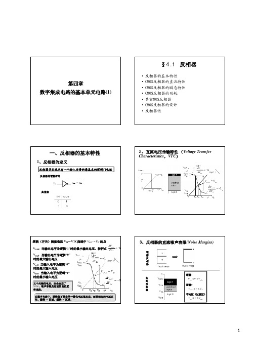
反相器VTC的特性:在过渡区有无限大的增益,门的阈值位于逻辑摆幅的中点,高电平和低电平噪声容限均等于这一摆幅的一半。
输入和输出阻抗为无限大和零。
t p:输入和输出波形的50%翻转点之间的时间。
第三章:电路符号:P63NMOS工作原理:笔记。
沟道长度调制效应使饱和区的电流不维持恒定状态,有微小的增加。
速度饱和:当沿沟道的电场达到某一临界值时,载流子的速度将由于散射效应而趋于饱和。
短沟期间比长沟器件更易进入饱和区。
MOS管开关模型:三个结论:1.电阻反比于器件的宽长比,晶体管的宽度加倍时将使电阻减半。
2.当V DD>V T +V DSAT/2时电阻实际上将与电压源电压无关。
3.一旦电源电压接近V T,电阻会急剧增加。
电容种类:1.MOS结构电容2.沟道电容3.结电容衬偏效应是V T值增加,原因是由于电荷数量变多(具体看课件)全比例缩小(恒电场缩小):电压和尺寸被缩小同一个因子S,可以提高器件密度,提高性能,降低功耗。
恒压缩小:尺寸缩小倍数为S,电压不变一般化缩小:工艺尺寸和电压各自独立缩小,尺寸缩小倍数为S,电压降低倍数为U。
第四章:集总模型:树结构链结构:传输线性质:信号以波的形式传播通过互联介质。
传输线分类:有损传输线,无损传输线P114 表格4.7第五章:有比反相器:在输出低电平时,驱动管和负载管同时导通,其输出低电平由驱动管的导通电阻和负载管的等效电阻分压决定。
无比反相器:在输出低电平是,只有驱动管导通,负载管截止,在理想情况下,其输出低电平为0推挽结构CMOS电路特点:VTC 特点:P133图开关阈值电压定义为Vin=V out的点,由可知,开关阈值取决于r,它是PMOS和NMOS相对驱动强度的比。
(整理)集成电路原理学习指南-第二版

沟道等效电阻
(1)与W/L反比,
(2)与电压有关,
(3)VDD大的时候较小(饱和工作区)
(4)VDD接近Vt的时候急剧增大
(5)一般使用工作区平均电阻
掌握
3.18
电阻的近似
平均电阻,并估算其误差(保守估计还是过估计)
掌握
3.19
结构电容
栅电容,覆盖电容
掌握
3.20
沟道电容
在不同工作区域的变化和原因,在阈值附近最小
f=Cext/Cint=Cext/γCg,尺寸决定电容,所以也是扇出尺寸,为工艺决定的系数,代表自电容与栅电容的关系
掌握
5.13
反相器链的最优尺寸设计
每一级为前后级的几何平均
扇出系数公式(5.35),公式(5.36)
掌握
5.14
最佳等效扇出
图5.21(pp 152),一般取4
掌握
5.15
上升下降时间对延时的影响
了解
3.26
电容估算
(1)栅电容,扩散电容大致相当(定义单位NMOS和PMOS的栅电容为C)
(2)它们随沟道宽度等比增加(kC)
(3)最小晶体管C值可初略估计为1fF/um宽度(65nm工艺,宽0.1um晶体管的C值约为0.1fF)
[Weste,4.3.2]
掌握
第四章导线
序号
概念
知识点和关键词
掌握程度
掌握
3.13
MOS IV特性
画出IV图,标出工作区,图3.24(pp 74)
掌握并会定性画图
3.14
手工分析的局限
在电阻区和过度区之间的区域偏差较大
了解
3.15
设计测试点验证IV
知道晶体管几个端口的电压,固定哪个,量哪个电流,可以提取以上列出的某个参数。
数字集成电路设计第4章

8
Wires
Capacitance of Wire Interconnect
VDD
VDD
M2
V in
C gd12
C db2
C g4
Vout
M4 V out2
Cdb1 Cw
C g3
M1
M3
In te rc o n n e c t
V in S im p lifie d
M odel
© DEEig1i4ta1l Integrated Circuits2nd
© DEEig1i4ta1l Integrated Circuits2nd
24
Wires
趋效应
这一效应可以近似假设为电流均匀流过这个导体的 厚度为δ的外壳,如下图所示:
假设导线的总截面现在局限在大约2(W+H) δ,那么 高频(f>fs时)时电阻表达式如下:
这里
© DEEig1i4ta1l Integrated Circuits2nd
15
Wires
多层互连结构的影响
在多层互连结构中导线间 的电容已成为主要因素。
随特征尺寸的缩小,导线 间电容在总电容中所占比例 增加,如右图可以得到最好 的说明。
当W变成小于1.75H时, 导线间电容开始占主导地位 。
© DEEig1i4ta1l Integrated Circuits2nd
16
Wires
27
Wires
Example: Intel 0.25 micron Process
5 metal layers Ti/Al - Cu/Ti/TiN Polysilicon dielectric
© DEEig1i4ta1l Integrated Circuits2nd
数字集成电路--电路、系统与设计(第二版)复习资料
第一章数字集成电路介绍第一个晶体管,Bell 实验室,1947第一个集成电路,Jack Kilby ,德州仪器,1958 摩尔定律:1965年,Gordon Moore 预言单个芯片上晶体管的数目每18到24个月翻一番。
(随时间呈指数增长)抽象层次:器件、电路、门、功能模块和系统 抽象即在每一个设计层次上,一个复杂模块的内部细节可以被抽象化并用一个黑匣子或模型来代替。
这一模型含有用来在下一层次上处理这一模块所需要的所有信息。
固定成本(非重复性费用)与销售量无关;设计所花费的时间和人工;受设计复杂性、设计技术难度以及设计人员产出率的影响;对于小批量产品,起主导作用。
可变成本 (重复性费用)与产品的产量成正比;直接用于制造产品的费用;包括产品所用部件的成本、组装费用以及测试费用。
每个集成电路的成本=每个集成电路的可变成本+固定成本/产量。
可变成本=(芯片成本+芯片测试成本+封装成本)/最终测试的成品率。
《一个门对噪声的灵敏度是由噪声容限NM L (低电平噪声容限)和NM H (高电平噪声容限)来度量的。
为使一个数字电路能工作,噪声容限应当大于零,并且越大越好。
NM H = V OH - V IH NM L = V IL - V OL 再生性保证一个受干扰的信号在通过若干逻辑级后逐渐收敛回到额定电平中的一个。
一个门的VTC 应当具有一个增益绝对值大于1的过渡区(即不确定区),该过渡区以两个有效的区域为界,合法区域的增益应当小于1。
理想数字门 特性:在过渡区有无限大的增益;门的阈值位于逻辑摆幅的中点;高电平和低电平噪声容限均等于这一摆幅的一半;输入和输出阻抗分别为无穷大和零。
传播延时、上升和下降时间的定义传播延时tp 定义了它对输入端信号变化的响应有多快。
它表示一个信号通过一个门时所经历的延时,定义为输入和输出波形的50%翻转点之间的时间。
上升和下降时间定义为在波形的10%和90%之间。
对于给定的工艺和门的拓扑结构,功耗和延时的乘积一般为一常数。
数字集成电路--电路、系统与设计(第二版)课后练习题-第四章 导线-Chapter 4 The Wire

1Chapter 4 Problem SetChapter 4Problems1.[M, None, 4.x] Figure 0.1 shows a clock-distribution network. Each segment of the clock net-work (between the nodes) is 5 mm long, 3 μm wide, and is implemented in polysilicon. Ateach of the terminal nodes (such as R ) resides a load capacitance of 100 fF.a.Determine the average current of the clock driver, given a voltage swing on the clock linesof 5 V and a maximum delay of 5 nsec between clock source and destination node R . Forthis part, you may ignore the resistance and inductance of the networkb.Unfortunately the resistance of the polysilicon cannot be ignored. Assume that eachstraight segment of the network can be modeled as a Π-network. Draw the equivalent cir-cuit and annotate the values of resistors and capacitors.c.Determine the dominant time-constant of the clock response at node R .2.[C, SPICE, 4.x] You are designing a clock distribution network in which it is critical to mini-mize skew between local clocks (CLK 1, CLK 2, and CLK 3). You have extracted the RC net-work of F igure 0.2, which models the routing parasitics of your clock line. Initially, you notice that the path to CLK 3 is shorter than to CLK 1 or CLK 2. In order to compensate for this imbalance, you insert a transmission gate in the path of CLK 3 to eliminate the skew.a.Write expressions for the time-constants associated with nodes CLK 1,CLK 2 and CLK 3.Assume the transmission gate can be modeled as a resistance R 3.b.If R 1 = R 2 = R 4 = R 5 = R and C 1 = C 2 = C 3 = C 4 = C 5 = C , what value of R 3 is required to balance the delays to CLK 1, CLK 2, and CLK 3?c.For R =750Ω and C =200fF, what (W /L )’s are required in the transmission gate to elimi-nate skew? Determine the value of the propagation delay.d.Simulate the network using SPICE, and compare the obtained results with the manually obtained numbers.3.[M, None, 4.x]Consider a CMOS inverter followed by a wire of length L . Assume that in thereference design, inverter and wire contribute equally to the total propagation delay t pref . Youmay assume that the transistors are velocity-saturated. The wire is scaled in line with the idealwire scaling model . Assume initially that the wire is a local wire .a.Determine the new (total) propagation delay as a a function of t p ref , assuming that technol-ogy and supply voltage scale with a factor 2. Consider only first-order effects.b.Perform the same analysis, assuming now that the wire scales a global wire , and the wire length scales inversely proportional to the technology.Figure 0.1Clock-distribution network.SR2Chapter 4 Problem Setc.Repeat b, but assume now that the wire is scaled along the constant resistance model. You may ignore the effect of the fringing capacitance.d.Repeat b, but assume that the new technology uses a better wiring material that reduces the resistivity by half, and a dielectric with a 25% smaller permittivity.e.Discuss the energy dissipation of part a. as a function of the energy dissipation of the orig-inal design E ref .f.Determine for each of the statements below if it is true, false, or undefined, and explain in one line your answer. - When driving a small fan-out, increasing the driver transistor sizes raises the short-circuit power dissipation. - Reducing the supply voltage, while keeping the threshold voltage constant decreases the short-circuit power dissipation.- Moving to Copper wires on a chip will enable us to build faster adders.- Making a wire wider helps to reduce its RC delay.- Going to dielectrics with a lower permittivity will make RC wire delay more impor-tant.4.[M, None, 4.x] A two-stage buffer is used to drive a metal wire of 1 cm. The first inverter is of minimum size with an input capacitance Ci=10 fF and an internal propagation delay t p0=50 ps and load dependent delay of 5ps/fF. The width of the metal wire is 3.6 μm. The sheet resis-tance of the metal is 0.08 Ω/, the capacitance value is 0.03 fF/μm 2and the fringing field capacitance is 0.04fF/μm.a.What is the propagation delay of the metal wire?pute the optimal size of the second inverter. What is the minimum delay through the buffer?c.If the input to the first inverter has 25% chance of making a 0-to-1 transition, and the whole chip is running at 20MHz with a 2.5 supply voltage, then what’s the power con-sumed by the metal wire?5.[M, None, 4.x]To connect a processor to an external memory an off -chip connection is neces-sary. The copper wire on the board is 15 cm long and acts as a transmission line with a charac-teristic impedance of 100Ω.(See F igure 0.3). The memory input pins present a very highimpedance which can be considered infinite. The bus driver is a CMOS inverter consisting ofvery large devices: (50/0.25) for the NMOS and (150/0.25) for the PMOS, where all sizes areClock CLK 1CLK 2CLK 3R 1R 2R 5R 4R 3Model as:Figure 0.2RC clock-distribution network.driver C 1C 3C 4C 5C 2Digital Integrated Circuits - 2nd Ed3 in μm. The minimum size device, (0.25/0.25) for NMOS and (0.75/0.25) for PMOS, has theon resistance 35 kΩ.a.Determine the time it takes for a change in the signal to propagate from source to destina-tion (time of flight). The wire inductance per unit length equals 75*10-8 H/m.b.Determine how long it will take the output signal to stay within 10% of its final value. Youcan model the driver as a voltage source with the driving device acting as a series resis-tance. Assume a supply and step voltage of 2.5V. Hint: draw the lattice diagram for thetransmission line.c.Resize the dimensions of the driver to minimize the total delay.L=15cmMemoryZ=100ΩFigure 0.3The driver, the connecting copper wire and thememory block being accessed.6.[M, None, 4.x] A two stage buffer is used to drive a metal wire of 1 cm. The first inverter is aminimum size with an input capacitance C i=10 fF and a propagation delay t p0=175 ps whenloaded with an identical gate. The width of the metal wire is 3.6 μm. The sheet resistance ofthe metal is 0.08 Ω/, the capacitance value is 0.03 fF/μm2 and the fringing field capacitanceis 0.04 fF/μm.a.What is the propagation delay of the metal wire?pute the optimal size of the second inverter. What is the minimum delay through thebuffer?7.[M, None, 4.x] For the RC tree given in Figure 0.4 calculate the Elmore delay from node A tonode B using the values for the resistors and capacitors given in the below in Table 0.1.Figure 0.4RC tree for calculating the delay4Chapter 4 Problem SetTable 0.1Values of the components in the RC tree of Figure 0.4Resistor Value(Ω)Capacitor Value(fF)R10.25C1250R20.25C2750R30.50C3250R4100C4250R50.25C51000R6 1.00C6250R70.75C7500R81000C82508.[M, SPICE, 4.x] In this problem the various wire models and their respective accuracies willbe studied.pute the 0%-50% delay of a 500um x 0.5um wire with resistance of 0.08 Ω/,witharea capacitance of 30aF/um2, and fringing capacitance of 40aF/um. Assume the driverhas a 100Ω resistance and negligible output capacitance.•Using a lumped model for the wire.•Using a PI model for the wire, and the Elmore equations to find tau. (see Chapter 4, figure4.26).•Using the distributed RC line equations from Chapter 4, section 4.4.4.pare your results in part a. using spice (be sure to include the source resistance). Foreach simulation, measure the 0%-50% time for the output•First, simulate a step input to a lumped R-C circuit.•Next, simulate a step input to your wire as a PI model.•Unfortunately, our version of SPICE does not support the distributed RC model as described in your book (Chapter 4, section 4.5.1). Instead, simulate a step input to yourwire using a PI3 distributed RC model.9.[M, None, 4.x] A standard CMOS inverter drives an aluminum wire on the first metal layer.Assume Rn=4kΩ, Rp=6kΩ. Also, assume that the output capacitance of the inverter is negli-gible in comparison with the wire capacitance. The wire is .5um wide, and the resistivity is0.08 Ω/..a.What is the "critical length" of the wire?b.What is the equivalent capacitance of a wire of this length? (For your capacitance calcula-tions, use Table 4.2 of your book , assume there’s field oxide underneath and nothingabove the aluminum wire)Digital Integrated Circuits - 2nd Ed510.[M, None, 4.x] A 10cm long lossless transmission line on a PC board (relative dielectric con-stant = 9, relative permeability = 1) with characteristic impedance of 50Ω is driven by a 2.5Vpulse coming from a source with 150Ω resistance.a.If the load resistance is infinite, determine the time it takes for a change at the source toreach the load (time of flight).Now a 200Ω load is attached at the end of the transmission line.b.What is the voltage at the load at t = 3ns?c.Draw lattice diagram and sketch the voltage at the load as a function of time. Determinehow long does it take for the output to be within 1 percent of its final value.11.[C, SPICE, 4.x] Assume V DD =1.5V . Also, use short-channel transistor models forhand analy-sis.a.The Figure 0.5 shows an output driver feeding a 0.2 pF effective fan-out of CMOS gates through a transmission line. Size the two transistors of the driver to optimize the delay.Sketch waveforms of V S and V L , assuming a square wave input. Label critical voltages and times.b.Size down the transistors by m times (m is to be treated as a parameter). Derive a first order expression for the time it takes for V L to settle down within 10% of its final voltage pare the obtained result with the case where no inductance is associated with the wire.Please draw the waveforms of V L for both cases, and comment.e the transistors as in part a). Suppose C L is changed to 20pF. Sketch waveforms of V S and V L , assuming a square wave input. Label critical voltages and instants.d.Assume now that the transmission line is lossy. Perform Hspice simulation for three cases:R=100 Ω/cm; R=2.5 Ω/cm; R=0.5 Ω/cm. Get the waveforms of V S , V L and the middle point of the line. Discuss the results.12.[M, None, 4.x] Consider an isolated 2mm long and 1μm wide M1(Metal1)wire over a silicon substrate driven by an inverter that has zero resistance and parasitic output capccitance. How will the wire delay change for the following cases? Explain your reasoning in each case.a.If the wire width is doubled.b.If the wire length is halved.c.If the wire thickness is doubled.d.If thickness of the oxide between the M1 and the substrate is doubled.13.[E, None, 4.x] In an ideal scaling model, where all dimensions and voltages scale with a fac-tor of S >1 :L=350nH/m 10cm C=150pF/m inV DDV DD V S V LC L =0.2pF Figure 0.5Transmission line between two inverters6Chapter 4 Problem Seta.How does the delay of an inverter scale?b.If a chip is scaled from one technology to another where all wire dimensions,including thevertical one and spacing, scale with a factor of S, how does the wire delayscale? How doesthe overall operating frequency of a chip scale?c.Repeat b) for the case where everything scales, except the vertical dimension of wires (itstays constant).。
第4章 数字集成电路的基本单元电路1
VIH + VIL = VDD
具有相等的噪声 容限: NML= NMH
üVin= VDD,NMOS导通,PMOS截止 , 稳态Vout=0;
VDD
Vin = VDD
V out = 0
CMOS反相器的工作特点:
ü Vout=Vin; ü 稳态单管导通,没有直 通电流
反相器中 MOSFET的 工作 区域
Vout
N- O P-L N-S P-L N-L P-S
二、CMOS反相器的直流特性
低电平信号的噪声容限NML: NML= VIL- VOL
NM L
噪声影响下的数字信号传播
设在无噪声条件下,输入电压和输出电压间的关系为 VOUT = f (VIN ) 如果输入信号由于噪声而偏离额定值,则输出电压也会偏离 原先的额定值
' VOUT = f (VIN ) +
dVOUT ∆VIN + 高阶项(忽略) dVIN
1 Wp 2 µ pCox 2 (VIN − VDD − VTp ) (VOUT − VDD ) − (VOUT − VDD ) 2 Lp
K n (VIL − VTn ) = K p ( 2VOUT − VIL + VTp − VDD )
数字集成电路设计笔记归纳
数字集成电路设计笔记归纳第三章、器件⼀、超深亚微⽶⼯艺条件下MOS 管主要⼆阶效应:1、速度饱和效应:主要出现在短沟道NMOS 管,PMOS 速度饱和效应不显著。
主要原因是TH GS V V -太⼤。
在沟道电场强度不⾼时载流⼦速度正⽐于电场强度(µξν=),即载流⼦迁移率是常数。
但在电场强度很⾼时载流⼦的速度将由于散射效应⽽趋于饱和,不再随电场强度的增加⽽线性增加。
此时近似表达式为:µξυ=(c ξξ<),c s a t µξυυ==(c ξξ≥),出现饱和速度时的漏源电压DSAT V 是⼀个常数。
线性区的电流公式不变,但⼀旦达到DSAT V ,电流即可饱和,此时DS I与GS V 成线性关系(不再是低压时的平⽅关系)。
2、Latch-up 效应:由于单阱⼯艺的NPNP 结构,可能会出现VDD 到VSS 的短路⼤电流。
正反馈机制:PNP 微正向导通,射集电流反馈⼊NPN 的基极,电流放⼤后⼜反馈到PNP 的基极,再次放⼤加剧导通。
克服的⽅法:1、减少阱/衬底的寄⽣电阻,从⽽减少馈⼊基极的电流,于是削弱了正反馈。
2、保护环。
3、短沟道效应:在沟道较长时,沟道耗尽区主要来⾃MOS 场效应,⽽当沟道较短时,漏衬结(反偏)、源衬结的耗尽区将不可忽略,即栅下的⼀部分区域已被耗尽,只需要⼀个较⼩的阈值电压就⾜以引起强反型。
所以短沟时VT 随L 的减⼩⽽减⼩。
此外,提⾼漏源电压可以得到类似的效应,短沟时VT随VDS增加⽽减⼩,因为这增加了反偏漏衬结耗尽区的宽度。
这⼀效应被称为漏端感应源端势垒降低。
4、漏端感应源端势垒降低(DIBL):VDS增加会使源端势垒下降,沟道长度缩短会使源端势垒下降。
VDS很⼤时反偏漏衬结击穿,漏源穿通,将不受栅压控制。
5、亚阈值效应(弱反型导通):当电压低于阈值电压时MOS管已部分导通。
不存在导电沟道时源(n+)体(p)漏(n+)三端实际上形成了⼀个寄⽣的双极性晶体管。
数字集成电路分析和设计第四章答案
P4.1. Problem should refer to Figure P4.2.a. All inverters but the CMOS inverter consume static power then the output is high.Notice that in the first three inverters when the input is high, there is always a directconnection from V DD to G ND .b. None of the static inverters consumes power when the input is low because there is nopath from V DD to G ND .c. All inverters but the saturated enhancement inverter has a V OH of 1.2 V.d. Only the CMOS inverter has a V OL of 0 V.e. Except for the CMOS inverter, all the other inverte rs’ functionality depend on therelative sizes of the transistors.P4.2. Problem should refer to Figure P4.1a. Resistive loadb. Saturated-enhancement loadIterate to produce:To compute V OL we can ignore body effect and equate currents:Solve for 0.03OL V V ≈c. Linear-enhancement loadIterate to produce:This tells us that V GG should have been above 1.6V <closer to 1.7 V>.To compute V OL we can ignore body effect and equate currents. Note that the load issaturated even though we call it a linear-enhancement load. The driver is alsosaturated due to the device sizes used.Solve for 0.69V OL V ≈d. CMOSP4.3. For this problem, you are required to use the formulae:We already know that V OH =1.2 V and V OL =0 V. For V S use:Next V IL and V IH are estimated as follows:ThereforeWhen we cut the size of the PMOS device in half, the VTC shifts to the left. So V IL , V S , and V IH will all shift to the left. The recalculation of the switching threshold produces V S =0.566V. We can compute V IL to be roughly 0.533V and V IH to be roughly 0.667V.ThereforeP4.4. Similar approach as in P4.3. Run SPICE to check results.P4.5. First, set up the equation.Now solve for χ.This implies that a very large <W/L>P is needed to reach the desired value. It also reveals the limitations of the models. SPICE would be needed to obtain an acceptable solution if the switching threshold of 0.9V is truly desired.P4.6. SPICEP4.7. The advantages of the pseudo-PMOS is that it can reach a V OH of V DD while the pseudo-NMOS V OH can never reach that value. Additionally, the pseudo-NMOS’s V OH dependson the relative sizings of the inverters.The disadvantage is the dual of its advantage. The pseudo-PMOS inverter can never reach a V OL of 0 V. In addition, the pseudo-PMOS device will have to be approximately twice as large as a pseudo-NMOS device with comparable characteristics. This is due to the unequal mobility of holes and electrons. The pseudo-PMOS’s NMOS pull -down device is twice as strong as the pseudo-NMOS’s PMOS pull -up device, that means that the pseudo-PMOS’s PMOS wi ll have to be bigger than the NMOS device in a pseudo-NMOS.P4.8. a> Circuit is a buffer with degraded outputs.Output swing calculation:When IN DD V V =, output voltage is OH DD TN V V V =-. Since the source of NMOS transistor is not connected to substrate <ground>, we must take into account body effect.When 0IN V V =, output voltage is ||OL TP V V =. Since the source of PMOS transistor is not connected to substrate <V DD >, we must take into account body effect.Therefore the output swing is DD TN V V - to ||TP V with full accounting for body effect.b> Assume that the input is at 0 and the output is at |V TP |. As the input is increased, the output will stay constant until the NMOS device turns on. That will occur at V IN =|V TP |+V TN . The upper transistor behaves as a source follower and will pull the output along as the input rises until the output reaches V DD -V TN . However, as the input is reduced in value the output stays at its highvalue until the PMOS device turns on. This occurs at V IN=V DD-< |V TP|+V TN>. Then the PMOS device acts as a source follower and the output drops linearly to |V TP| as the input is reduced.c> The gain of the circuit is close to unity but slightly below this value. The circuit has poor noise rejection properties as it lacks the regenerative properties <this is a consequence of low gain>.d> SPICE run.P4.9.Resistive Load inverter:Saturated Enhancement Load inverter <ignoring body-effect>:Linear Enhancement Load inverter <ignoring body-effect>:The linear enhancement load inverter requires the largest pull-down device since it has the strongest pull up device. The resistive load inverter is next and the saturated enhancement load requires the smallest pull-down device.P4.10.We will illustrate the process and estimate the solutions for this problem.We already know that V OH=1.2 V and V OL=0 V. For V S use:Next V IL and V IH are estimated as follows:We can compute V IL to be roughly 0.533V.We can compute V IH to be roughly 0.667V.When we double the size of the PMOS device, the VTC shifts to the right. So V IL, V S, and V IH will all shift to the right. The recalculation of the switching threshold produces V S=0.6V.We can compute V IL to be roughly 0.55V and V IH to be roughly 0.65V.P4.11.The peak current would occur when both devices are in saturation and when V out=V in=V S.We can easily compute V S as:P4.12.As the required V OL becomes smaller, the W D/W L ratio becomes larger.P4.13.SPICEP4.14.The expression for the switching threshold of a CMOS inverter is:Solving for χ.Now solving for the ratio of sizes.Solving for χ.Now solving for the ratio of sizes.In the first case <0.6S DD V V >, the PMOS is much larger than the NMOS, so t PLH issmaller and t PHL is larger. The reverse is true for the second case.P4.15 <a> It does not have the regenerative property since the gain is less than one.<b> The last inverter would have an output of about 0.8V.<c> It is not possible to define the noise margin for this gate. Even a properinput eventually produces the incorrect output.P4.16 Both gates would work as a tristate buffer. However, as we shall find out in Chapter 7, the second one is prone to charge-sharing. That is, when the output is high and the EN signal is low, if the input goes high, the output may drop slightly in value due to loss of charge to the adjacent internal node.。
合肥工业大学_数字集成电路设计-第四章导线
材料
n, p 阱扩散区 n+, p+ 扩散区 n+, p+ 硅化物扩散区 n+, p+多晶硅 n+, p+硅化物多晶硅
铝
薄层电阻 (/ ) 1000 ~ 1500 50 ~ 150 3~5 150 ~ 200 4~5 0.05 ~ 0.1
半导体集成电路基础
2014
第4章 导线
合肥工业大学电子科学与应用物理学院
本章重点
1. 确定并定量化互连参数 2. 介绍互连线的电路模型 3. 导线的SPICE细节模型 4. 工艺尺寸缩小及它对互连的影响
导线. 2
合肥工业大学应用物理系
4.1 引言
• 由导线引起的寄生效应所显示的尺寸缩小特性并不与如晶体管等有 源器件相同,随着器件尺寸的缩小和电路速度的提高,它们常常变 得非常重要
• 导线相互间的电容可以被忽略,并且所有的寄生电容都可以模拟成 接地电容 – 当相邻导线间的间距很大时 – 当导线只在一段很短的距离上靠近在一起时
注意:有经验的设计者知道如何去区分主要和次要的效应
导线. 7
合肥工业大学应用物理系
4.3 互连参数:电容、电阻和电感
4.3.1 电容
• 一条导线的电容与它的形状、它周 围的情况、它与衬底的距离以及它 与周围导线的距离都有关系
• 利用先进的参数提取工具来获取一 个完整版图中互连线电容的精确值
导线. 8
合肥工业大学应用物理系
互连线的平行板电容模型
L
H tdi
current flow
electrical field lines W
dielectric (SiO2) substrate
permittivity constant (SiO2= 3.9)
数字集成电路知识点整理
Digital IC:数字集成电路是将元器件和连线集成于同一半导体芯片上而制成的数字逻辑电路或系统第一章引论1、数字IC芯片制造步骤设计:前端设计(行为设计、体系结构设计、结构设计)、后端设计(逻辑设计、电路设计、版图设计)制版:根据版图制作加工用的光刻版制造:划片:将圆片切割成一个一个的管芯(划片槽)封装:用金丝把管芯的压焊块(pad)与管壳的引脚相连测试:测试芯片的工作情况2、数字IC的设计方法分层设计思想:每个层次都由下一个层次的若干个模块组成,自顶向下每个层次、每个模块分别进行建模与验证SoC设计方法:IP模块(硬核(Hardcore)、软核(Softcore)、固核(Firmcore))与设计复用Foundry(代工)、Fabless(芯片设计)、Chipless(IP设计)“三足鼎立”——SoC发展的模式3、数字IC的质量评价标准(重点:成本、延时、功耗,还有能量啦可靠性啦驱动能力啦之类的)NRE (Non-Recurrent Engineering) 成本设计时间和投入,掩膜生产,样品生产一次性成本Recurrent 成本工艺制造(silicon processing),封装(packaging),测试(test)正比于产量一阶RC网路传播延时:正比于此电路下拉电阻和负载电容所形成的时间常数功耗:emmmm自己算4、EDA设计流程IP设计系统设计(SystemC)模块设计(verilog)综合版图设计(.ICC) 电路级设计(.v 基本不可读)综合过程中用到的文件类型(都是synopsys版权):可以相互转化.db(不可读).lib(可读)加了功耗信息.sdb .slib第二章器件基础1、保护IC的输入器件以抗静电荷(ESD保护)2、长沟道器件电压和电流的关系:3、短沟道器件电压和电流关系速度饱和:当沿着沟道的电场达到临界值ξC时,载流子的速度由于散射效应(载流子之间的碰撞)而趋于饱和。
- 1、下载文档前请自行甄别文档内容的完整性,平台不提供额外的编辑、内容补充、找答案等附加服务。
- 2、"仅部分预览"的文档,不可在线预览部分如存在完整性等问题,可反馈申请退款(可完整预览的文档不适用该条件!)。
- 3、如文档侵犯您的权益,请联系客服反馈,我们会尽快为您处理(人工客服工作时间:9:00-18:30)。
R1 •
R2
L R R□ A HW W
L
L
为了得到一条导线的电阻,只需 将薄层电阻乘以该导线的W/L比
导线. 16
合肥工业大学应用物理系
互连电阻设计数据
• 常用导体的电阻率 – IC中最常用的互连材料是铝
– 最先进的工艺正在越来越多地选择铜作为导体
材料 (-m) 材料 薄层电阻 (/)
导线. 3
合肥工业大学应用物理系
4.2 简介
• 当代最先进的工艺可以提供许多铝或铜金属层以及至少一层多晶。 甚至通常用来实现源区和漏区的重掺杂n+和p+扩散层也可以用来作 为导线 寄生参数对电路性能的影响 – 使传播延时增加,或者说相应于性能的下降 – 会影响能耗和功率的分布 – 会引起额外的噪声来源,从而影响电路的可靠性
• • 在非常高的频率下,趋肤效应使导线电阻变成与频率有关 高频电流倾向于主要在导线的表面流动,其电流密度随进入导体的 深度而呈指数下降 W δ= (/(f)) 其中f是频率 = 4 x 10⁻⁷ H/m 导线的总截面 ~ 2(W+H) • • •
导线. 19
H
= 2.6 m for Al at 1 GHz
i
•
RC 树的性质 – 仅有一个输入节点
Ci
– 在源节点s和该电路的任何节点i之间存在一条唯一的电阻路径
– 所有的电容都在某个节点和地之间
导线. 24 合肥工业大学应用物理系
s • 路径电阻
R1 C1
R2
1
2
C2
4
R3 R 4
C3
3
C4 Ri
i
– 从源节点s和该电路的任何节点i之间的总电阻
Rii R j R j paths i
4.3 互连参数:电容、电阻和电感
4.3.1 电容
• 一条导线的电容与它的形状、它周 围的情况、它与衬底的距离以及它 与周围导线的距离都有关系 利用先进的参数提取工具来获取一 个完整版图中互连线电容的精确值
•
导线. 8
合肥工业大学应用物理系
互连线的平行板电容模型
current flow
L
electrical field lines W
高频时电阻的增加可以引起在导线上传送的信号有额外的衰减,并 因此产生失真 fs = 4 / ( (max(W,H))2) –趋肤效应的发生在趋肤深度等于导体最大尺 寸(W或L)一半时的频率 趋肤效应是对较宽导线才有的问题,如时钟信号
合肥工业大学应用物理系
例4.3 趋肤效应和铝导线
趋肤效应对现代集成电路的影响 下图画出了对于各种宽度的铝导体趋肤效应引起的电阻增加
• 采用只含电容的模型 – 当导线很短,导线的截面很大时 – 当所采用的互连材料电阻率很低时 • 导线相互间的电容可以被忽略,并且所有的寄生电容都可以模拟成 接地电容
– 当相邻导线间的间距很大时
– 当导线只在一段很短的距离上靠近在一起时
注意:有经验的设计者知道如何去区分主要和次要的效应
导线. 7 合肥工业大学应用物理系
导线. 10 合肥工业大学应用物理系
边缘场电容的影响
(from [Bakoglu89])
图4.5 包括边缘场效应时互连线电容与W/tdi的关系
导线. 11 合肥工业大学应用物理系
多层互连结构中导线间的电容耦合
fringing
parallel
注意:这些浮空电容不仅形成噪声源(串扰),而且对电路性能也有负 面影响
j 1
i
Ci
•
共享的路径电阻 – 从根节点s至节点k和节点i这两条路径共享的电阻
N
Rik R j R j paths i paths k
j 1
•
在节点i 处的Elmore延时由下式给出:
Di C k Rik
k 1
N
导线. 25
合肥工业大学应用物理系
Al2
Al3
Al4
Al5
Interwire Cap
导线. 14
40
95
85
85
85
115
per unit wire length in aF/m for minimally-spaced wires 合肥工业大学应用物理系
例4.1 金属导线电容
考虑一条布置在第一层铝上的10cm长,1m宽的铝线,计算总的电容值。 平面(平行板)电容: ( 0.1×10⁶m2 )×30aF/m2 = 3pF 边缘电容: 总电容: 2×( 0.1×10⁶m )×40aF/m = 8pF 11pF
例4.6 树结构网络的RC延时
R1 R2
1 2
s
C2
4
C1
R3 R 4
C3
3
C4
Ri
i
Ci 节点i的Elmore延时:
Di = R1C1 + R1C2 + (R1+R3) C3 + (R1+R3) C4 + (R1+R3+Ri) Ci
导线. 26
合肥工业大学应用物理系
RC链的Elmore延时
D1 C1 R1
例4.2 金属线的电阻
考虑一条布置在第一层铝上的10cm长,1m宽的铝线。假设铝层的薄层 电阻为0.075Ω/□,计算导线的总电阻: Rwire=0.075Ω/□(0.1106m)/(1m)=7.5kΩ 分析:如果采用多晶或硅化物多晶来实现,……
导线. 18 合肥工业大学应用物理系
趋肤效应
分析:这些数字甚至连最低性能的数字电路也不能接受
导线. 23 合肥工业大学应用物理系
4.4.3 集总RC模型
• 把每段导线的总导线电阻集总成一个电阻R,并且同样把总的电容 合成一个电容C
•
适用于短导线,它对于长互连线是一个保守和不精确的模型
s R1 C1 R2
1 2
C2
4
R3 R 4
C3
3
C4 Ri
pp in aF/m2 fringe in aF/m
Al3
Al4 Al5
8.9
18 6.5 14 5.2 12
9.4
19 6.8 15 5.4 12
10
20 7 15 5.4 12
15
27 8.9 18 6.6 14
41
49 15 27 9.1 19 35 45 14 27 38 52
Poly
Al1
r1
Vin c1 1
D 2 C1 R1 C2 R1 R2
r2
c2 2 ri-1 ci-1 i-1
ri
ci
i
rN
cN
N
VN
Di C1 R1 C2 R1 R2 ... Ci R1 R2 ... Ri
Elmore延时公式
DN = C i R= j C i Rii
•
说明:设计者对于导线的寄生效应、它们的相对重要性以及它们的模 型有一个清晰的理解是非常重要的
导线. 4
合肥工业大学应用物理系
导线
发送器 电路图
接收器
实际视图
图4.1 总线网络中导线的电路表示及实际视图
导线. 5 合肥工业大学应用物理系
导线模型
• 一个考虑互连线寄生电容、电阻和电感的完整的电路模型
0.69 RC
RC 2.2 RC 2.3 RC
0.38 RC
0.5 RC 0.9 RC 1.0 RC
使用集总电容模型,源电阻RDriver=10 k,总的集总电容Clumped= 11 pF
t50% = 0.69 10 k 11pF = 76 ns t90% = 2.2 10 k 11pF = 242 ns
1000
for H = .70 m
W = 1 m W = 10 m W = 20 m
% Increase in Resistance
100
10
1
0.1
1E8
1E9
1E10
Frequency (Hz)
分析:1GHz时一条20m宽的导线的电阻增加30% ,而一条1m宽的导线 的电阻只增加2%
• 布线层之间的转接将给导线带来额外的电阻 – 尽可能地使信号线保持在同一层上并避免过多的接触或通孔
– 使接触孔较大可以降低接触电阻(电流集聚在实际中将限制接触 孔的最大尺寸)
• 典型接触电阻,RC, (最小尺寸)
– 金属或多晶至n+、p+以及金属至多晶为 5 ~ 20
– 通孔(金属至金属接触)为1 ~ 5
银 (Ag)
铜 (Cu) 金 (Au) 铝 (Al) 钨 (W)
1.6 x 10⁻⁸
1.7 x 10⁻⁸ 2.2 x 10⁻⁸ 2.7 x 10⁻⁸ 5.5 x 10⁻⁸
n, p 阱扩散区
n+, p+ 扩散区 n+, p+ 硅化物扩散区
1000 ~ 1500
50 ~ 150 3~5
n+, p+多晶硅
capacitance per unit length
导线. 22 合肥工业大学应用物理系
例4.5 导线的集总电容模型
假设电源内阻为10kΩ的一个驱动器,用来驱动一条10cm长,1m宽的 Al1导线。
电压范围 集总RC网络 分布RC网络
0 50% (tp)
0 63% () 10% 90% (tr) 0 90%
现假设第二条导线布置在第一条旁边,它们之间只相隔最小允许的距离, 计算其耦合电容。 耦合电容: Cinter = ( 0.1×10⁶m )×95 aF/m2 = 9.5pF