最详细的PM66芯片使用手册20131214
ICMF062P250MFR Common Mode Filter 数据手册说明书
4. 1 PART NUMBER CODE ICMF 06 2P 250 M F R ① ② ③ ④ ⑤⑥ ⑦
① Series name of ICT’s Common Mode Filter ② Dimensions, 0.87mm (L) ⅹ 0.67mm (W) ③ The Number of lines, 2P = 2 lines ④ Common Mode Impedance (at 100MHz), 25 ⅹ 100= 25Ω ⑤ Tolerance of common mode impedance, M= ±25% ⑥ Type of electrode plating: F= Lead Free ⑦ Packing Type, R= Reel
3. APPLICATIONS
• LVDS lines in notebook computers • USB2.0, IEEE1394, DVI, HDMI lines in PDP, LCD TV, DVD Player, PC, Audio player, DSC • MDDI, MIPI in mobile phone
4028
750
3230
325
3768
490
4038
760
L-box + 10S-box 380 x 370 x 200
Total(g) Chip(g)
6147 7503 8043 6177 7523 8063
620 960 1500 650 980 1520
<PQ Box>
Packing box + Product weight
Product CMF CMEF
SUSS PM5 手动芯片探测系统说明书
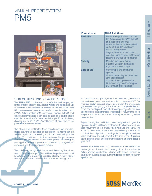
L i t h o g r a p h y W a f e r B o n d i n gD e v i c e B o n d i n g T e s t i n g MANUAL PROBE SYSTEMPM5Cost-Effective, Manual Wafer ProbingThe SUSS PM 5 is the most cost-effective and simple, yet highly precise, probing solution for wafers and substrates up to 150 mm. Great application flexibility is ensured for DC and HF measurements, device and wafer characterization tests (DWC), failure analysis (FA), submicron probing, M EM S and opto engineering tests. It can also be used as a flexible probe card for special wafer level reliability (WLR) applications, allowing up to 20 SUSS ProbeHeads TM at one time to be placed on the stable platen.The platen drive distributes force equally over two massive,All microscope lift options, manual or pneumatic, are easy to use and allow convenient access to the probes and DUT. Our modular design concept allows us to mount the microscope you require thus giving you the freedom to upgrade the sys-tem from the simplest manual microscope stages to the most sophisticated programmable microscope movements or to simply add a non-contact vibration analyzer for testing MEMS on wafer level.Ergonomically, the PM 5 has been designed with you, the operator, in mind. All knobs are located to allow easy and pre-cise movement of the chuck stage with just one hand. The X and Y axes can be adjusted independently. Once it has reached the test position, the stage locks into place and pro-vides additional fine adjustment in the Z direction. A pull-out stage permits quick and ergonomic loading and unloading of your DUT.The PM5 can be outfitted with a number of SUSS accessories and upgrades. These include, among others, laser cutters for failure analysis applications, chucks with special designs for calibration substrates and burnishing pads for high frequency applications.Technical Data: PM5 Manual Probe StationSUSS MicroTec Test Systems Worldwide Contacts: SUSS MicroTec Test Systems+49-35240-730 SUSS MicroTec China+86-21-5234-0432Design verification with SUSS PM5 MEMS testing with SUSS PM5and Polytec MSA 400Testing HF on PM5 (for small budgets).Dresden .Hsin-Chu .Munich .Saint Je oire.Santa Clara .Shanghai .Te mpe.Vaihinge n .Wate rbury Ce nte r .Yokohama。
mGreen 芯片模组说明书

mGreen 芯片模组使用说明书C2C Link 公司Jan Jan..02,201201221.简介mGreen 芯片模组是用来产生532-nm 绿光的单一组件。
采用808-nm 半导体激光器(LD )直接泵浦mGreen 芯片模组的简单结构,即可轻松获得500-1000mW 的绿光输出。
2.mGreen 芯片模组介绍如图1所示,mGreen 芯片模组由4个部件组成:硅基片,掺杂浓度为1%的Nd:YVO 4晶体,掺杂浓度为5mol%的MgO:PPLN 晶体和铜盖。
Nd:YVO 4晶体和MgO:PPLN 晶体经高精度准直固定在硅基片上,因此两个晶体的通光面严格平行。
Nd:YVO 4晶体和MgO:PPLN 晶体的光轴准直于竖直方向。
Nd:YVO 4晶体的入射面镀膜为HT@808nm ,HR@1064nm &532nm 。
MgO:PPLN 晶体的出射面镀膜为HR@1064nm ,HT@532nm 。
mGreen 芯片模组的尺寸为7(长)×4.5(宽)×2(厚)mm 3(即体积为0.063cm 3)。
图1.mGreen 芯片模组的3D 视图3.基于mGreen 芯片模组的绿光激光器结构采用mGreen 芯片模组制作激光器(laser head ),最基本的配置需求是一个硅基片MgO:PPLN 晶体Nd:YVO 4晶体铜盖作为泵浦源的808-nm 半导体激光器(c-mount 或者F-mount ),一个mGreen 芯片模组和相关配件(如半导体制冷片,热敏电阻和金属结构件等)。
图2给出了基于mGreen 芯片模组,808-nm 半导体激光器(c-mount )作为泵浦源的绿光激光器3D 视图。
值得注意的是,1.为了获得mGreen 芯片模组的最佳性能,对于偏振态为TE 的808-nm 半导体激光器需要旋转90度;2.mGreen 芯片模组的硅基片需要和热沉或半导体制冷片接触良好,以确保满足激光器工作要求的散热条件;3.mGreen 芯片模组同808-nm 半导体激光器之间的距离约为1mm ;4.无需聚焦镜和输出耦合镜;5.为保证较好的光束质量和功率转换效率,最好采用带快轴整形的808-nm 半导体激光器作为泵浦源,其光束在水平和竖直两个方向的发散角约为7度,光斑为方形。
最详细的PM66芯片使用手册20131214
描述 触収输入引脚(低有效)
输出引脚 接喇叭两端
电源正端 电源地 系统复位端(低有效) 编程控制端
-5-
PM66DATASHEET
2 PM66 的典型应用电路及 MCU 控制方式
2.1 典型线路
图 1 并行按键模式,PWM* 音频输出方式接线图
6K
32 100 200 400 800 1600 3200
8K
24 75 150 300 600 1200 2400
10K
19.2 60 120 240 480 960 1920
12K
16 50 100 200 400 800 1600
16K
12 37.5 75 150 300 600 1200
20K
4.3.1 关于静音(MUTE)的使用.................................................................................................. - 23 4.3.2 关于 Group <<组>>的应用.................................................................................................... - 24 5. FAQ ...................................................................................................................................................... - 26 -
PM66语音芯片资料
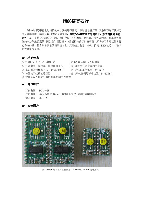
PM66语音芯片PM66系列是中青世纪科技公司于2009年推出的一款智能语音产品。
该系列芯片在使用方式及外部电路上基本可以和PM50系列兼容,但较PM50具有录音时间更长,放音音质更佳的优势,是一个整合了录放音电路,快闪存储,ADPCM编、解码器,功率放大器,稳压器等线路的全功能录放系统。
因为我们已经把它包装成标准的COB-28管脚,所以使用者可以很方便的将PM66设计整合到需要录放音的场合上,只需接上电源、喇叭、按键,PM66就是一个独立的声音播放系统。
★功能特点◎存储时间长 ( 40~4000秒) ◎ 8个输入脚,4个输出脚◎ 仅需电源、扬声器、按键即可工作◎ 自由组合录音段和声音段◎ 宽范围的采样频率 ( 4k~20kHz ) ◎ 弹性的工作电压( 3~5V )◎内置抗干扰精密稳压器◎ 多种LED闪烁频率设置( 1~12Hz )◎ 按键触发及串并行微控制器控制工作模式★电气特性工作电压: DC 3~5V工作电流:最大不超过 60 mA(PWM输出方式、接8欧姆喇叭时)静态电流:小于 2 uA★实物图片图1 PM66语音芯片实物图片(有DIP28,DIP16两种封装)图2 PM66编程器实物图1 PM66语音芯片型号及引脚定义(1)PM66系列按照录音时间区分,共有6种产品型号,下表为各种型号在不同的采样频率下可存放的时间对照表。
(2)PM66引脚定义及实际图片2 PM66的典型应用电路及控制方式(1)、并行模式、按键操作在PM66系列芯片的并行控制方式下可以分8段语音录放,K1~K8脚可以分别触发与其对应的8段语音(低有效),在烧录芯片的时候,可以设置为下降沿触发或者低电平触发。
K1~K8端口有内置上拉电阻和防抖动设计,可直接外接按键来触发放音。
也可用单片机口线直接对其操作。
如图1:图1 并行按键模式,PMW音频输出方式接线图连接扬声器的两种方式(PWM和DAC)音频输出方式的选择,首先需要在编程软件中设定,烧写芯片后按照以下说明连接。
优利德 UPO1204X-E系列数据手册 说明书
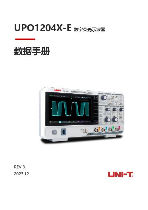
UPO1204X-E数字荧光示波器数据手册REV32023.12⏹模拟通道带宽:200MHz⏹模拟通道数:4⏹最大采样率:2GSa/s⏹垂直档位:500μV/div-20V/div⏹低底噪声:<100μVrms⏹最大存储深度可达28Mpts⏹波形捕获率最高300,000wfms/s⏹硬件实时波形不间断录制60,000帧⏹可自动测量36种波形参数,测量范围可选:屏幕或光标区域⏹支持7位硬件频率计测量⏹DVM支持交直流真有效值测量⏹波形运算功能(FFT、加、减、乘、除、数字滤波、逻辑运算和高级运算)⏹1M点增强FFT功能,支持频率设置,瀑布图,检波设置和标记测量等⏹丰富的触发功能(边沿,脉宽,视频,斜率,欠幅脉冲,超幅脉冲,延迟,超时,持续时间,建立保持、第N边沿和码型触发)⏹标配RS232、I2C、SPI触发⏹标配RS232、I2C、SPI全内存硬件实时解码⏹Ultra Phosphor超级荧光显示效果,高达256级的灰度显示⏹7英寸WVGA(800×480)TFT液晶屏⏹丰富的接口:USB Host、USB Device、LAN、EXT Trig、AUX Out(Trig Out、Pass/Fail、DVM)⏹支持波形导航、标记、段⏹支持SCPI可编程仪器标准命令⏹支持WEB访问和控制UPO1204X-E数字示波器采用了UNI-T新创的数字三维技术Ultra Phosphor2.0,全新外观升级,可实现深存储,高波形捕获率,实时波形录制与回放,256级灰度显示等功能;该款配置200MHz带宽,实时采样率高达2GSa/s,标配4通道,标配最大存储深度28Mpts,Fast Acquire模式下最高可达300,000wfms/s,硬件实时波形不间断录制和波形分析功能最大达6万帧波形;支持DVM模块,拥有丰富的触发和总线解码功能,并支持全内存硬件实时解码;广泛应用包括通信,半导体,计算机,集成电路设计,仪器仪表,工业电子,消费电子,汽车电子,现场维修,研发/教育等众多领域。
PMK 8 PMK 6 PMK 3 快速启动向导说明书
Back Can SSteel Back Can for PCI and QCI In-Ceiling Loudspeakers PMK 8Pre-Mount Kit for QCI and PCI 8" In-Ceiling Loudspeakers PMK 6Pre-Mount Kit for QCI and PCI 6" In-Ceiling Loudspeakers PMK 3Pre-Mount Kit for QCI 3" In-Ceiling LoudspeakersV 1.0带有此标志的终端设备具有强大的电流, 存在触电危险。
仅限使用带有 ¼'' TS 或扭锁式插头的高品质专业扬声器线。
所有的安装或调整均须由合格的专业人员进行。
此标志提醒您, 产品内存在未绝缘的危险电压, 有触电危险。
此标志提醒您查阅所附的重要的使用及维修说明。
请阅读有关手册。
小心为避免触电危险, 请勿打开机顶盖 (或背面挡板)。
设备内没有可供用户维修使用的部件。
请将维修事项交由合格的专业人员进行。
小心为避免着火或触电危险, 请勿将此设备置于雨淋或潮湿中。
此设备也不可受液体滴溅, 盛有液体的容器也不可置于其上, 如花瓶等。
小心维修说明仅是给合格的专业维修人员使用的。
为避免触电危险, 除了使用说明书提到的以外, 请勿进行任何其它维修。
所有维修均须由合格的专业人员进行。
1. 请阅读这些说明。
2. 请妥善保存这些说明。
3. 请注意所有的警示。
4. 请遵守所有的说明。
5. 请勿在靠近水的地方使用本产品。
6. 请用干布清洁本产品。
7. 请勿堵塞通风口。
安装本产品时请遵照厂家的说明。
8. 请勿将本产品安装在热源附近,如 暖 气 片, 炉子或其它产生热量的设备( 包 括功放器)。
9. 请勿移除极性插头或接地插头的安全装置。
接地插头是由两个插塞接点及一个接地头构成。
ST PM6611N 数据手册
Data briefFor further information contact your local STMicroelectronics sales office.February 2012Doc ID 022764 Rev 11/8PM6611N2 to 4-cell Li-ion, Li-FePO 4 battery charger with SMBus interface, N-channel RBFET and BATFET MOSFET selectorsFeatures■Buck converter–Synchronous buck converter with N-channel high-side, low-side Power MOSFET integrated drivers–350 kHz or 700 kHz switching frequency, selectable with SMBus–AC adapter input voltage range 9 V - 24 V – 5 V bias input voltage supply–Battery charge voltage range 2.5 V - 18 V –±0.5% charge voltage accuracy –0.1% cell charge voltage resolution –±3% charge current accuracy–Overvoltage, overcurrent protection–Battery, inductor, Power MOSFET short- circuit protection–Internal loop compensation network –Integrated soft-start■Selector–N-channel BATFET MOSFET driver–N-channel ACFET and RBFET MOSFET driver ■System– 1 mA quiescent supply current–17 µA - 35 µA sleep mode current (BATFET charge pump OFF - ON)–Thermal shutdownApplications■Mobile PC:–UMPC/MID and tablets–Netbook and notebook computersDescriptionThe PM6611N is a high efficiency battery charger with SMBus communication interface. It includes a synchronous switching DC-DC converter withMOSFET drivers. The possibility to set theswitching frequency with SMBus by choosing one of the two preset values of 350 kHz or 700 kHz assures the best trade-off between powerconversion efficiency and application component cost and pcb size.Integrated loop compensation network and soft-start allow the reduction of the number of external components.The PM6611N integrates 2 charge pumps to drive N-channel BATFET and ACFET - RBFET MOSFETs.The SMBus communication interface is used to set the battery charge current and voltage. The PM6611N charges 2 to 4-series Li-Ion or LiFePO 4 cells, for mobile PC applications. It is available in a 16-pin, 3x3 mm, QFN package.Table 1.Device summaryOrder codePackage Packing PM6611NQFN 3x3x1.0 16LTape and reelTypical application circuitPM6611N2/8Doc ID 022764 Rev 11 Typical application circuitPM6611N Device pinoutDoc ID 022764 Rev 13/82 Device pinoutPackage mechanical data PM6611N 3 Package mechanical dataIn order to meet environmental requirements, ST offers these devices in different grades ofECOP ACK® packages, depending on their level of environmental compliance. ECOPACKspecifications, grade definitions and product status are available at: . ECOPACKis an ST trademark.Table 2.QFN 3x3x1.0 16L mechanical datamm.Dim.Min.Typ.Max.A0.800.90 1.00A10.020.05A20.65 1.00A30.20b0.180.250.30D 2.85 3.00 3.15D1 1.50D2See T able3E 2.85 3.00 3.15E1 1.50E2See T able3e0.450.500.55L0.300.400.50ddd0.08Table 3.Exposed pad variationD2E2VariationMin.Typ.Max.Min.Typ.Min.A0.95 1.10 1.250.95 1.10 1.25B 1.45 1.60 1.75 1.45 1.60 1.754/8Doc ID 022764 Rev 1PM6611N Package mechanical dataDoc ID 022764 Rev 15/8Package mechanical data PM6611N6/8Doc ID 022764 Rev 1PM6611N Revision historyDoc ID 022764 Rev 17/84 Revision historyTable 4.Document revision historyDate RevisionChanges01-Feb-20121Initial release.PM6611NPlease Read Carefully:Information in this document is provided solely in connection with ST products. STMicroelectronics NV and its subsidiaries (“ST”) reserve the right to make changes, corrections, modifications or improvements, to this document, and the products and services described herein at any time, without notice.All ST products are sold pursuant to ST’s terms and conditions of sale.Purchasers are solely responsible for the choice, selection and use of the ST products and services described herein, and ST assumes no liability whatsoever relating to the choice, selection or use of the ST products and services described herein.No license, express or implied, by estoppel or otherwise, to any intellectual property rights is granted under this document. If any part of this document refers to any third party products or services it shall not be deemed a license grant by ST for the use of such third party products or services, or any intellectual property contained therein or considered as a warranty covering the use in any manner whatsoever of such third party products or services or any intellectual property contained therein.UNLESS OTHERWISE SET FORTH IN ST’S TERMS AND CONDITIONS OF SALE ST DISCLAIMS ANY EXPRESS OR IMPLIED WARRANTY WITH RESPECT TO THE USE AND/OR SALE OF ST PRODUCTS INCLUDING WITHOUT LIMITATION IMPLIED WARRANTIES OF MERCHANTABILITY, FITNESS FOR A PARTICULAR PURPOSE (AND THEIR EQUIVALENTS UNDER THE LAWS OF ANY JURISDICTION), OR INFRINGEMENT OF ANY PATENT, COPYRIGHT OR OTHER INTELLECTUAL PROPERTY RIGHT. UNLESS EXPRESSLY APPROVED IN WRITING BY TWO AUTHORIZED ST REPRESENTATIVES, ST PRODUCTS ARE NOT RECOMMENDED, AUTHORIZED OR WARRANTED FOR USE IN MILITARY, AIR CRAFT, SPACE, LIFE SAVING, OR LIFE SUSTAINING APPLICATIONS, NOR IN PRODUCTS OR SYSTEMS WHERE FAILURE OR MALFUNCTION MAY RESULT IN PERSONAL INJURY, DEATH, OR SEVERE PROPERTY OR ENVIRONMENTAL DAMAGE. ST PRODUCTS WHICH ARE NOT SPECIFIED AS "AUTOMOTIVE GRADE" MAY ONLY BE USED IN AUTOMOTIVE APPLICATIONS AT USER’S OWN RISK.Resale of ST products with provisions different from the statements and/or technical features set forth in this document shall immediately void any warranty granted by ST for the ST product or service described herein and shall not create or extend in any manner whatsoever, any liability of ST.ST and the ST logo are trademarks or registered trademarks of ST in various countries.Information in this document supersedes and replaces all information previously supplied.The ST logo is a registered trademark of STMicroelectronics. All other names are the property of their respective owners.© 2012 STMicroelectronics - All rights reservedSTMicroelectronics group of companiesAustralia - Belgium - Brazil - Canada - China - Czech Republic - Finland - France - Germany - Hong Kong - India - Israel - Italy - Japan - Malaysia - Malta - Morocco - Philippines - Singapore - Spain - Sweden - Switzerland - United Kingdom - United States of America8/8Doc ID 022764 Rev 1。
PM66芯片使用手册及参数
K1 = 1; } else {
K1 = 0; } k1_data = k1_data>>1; delay_1(76); K2 = 1; delay_1(76);//发码频率(500HZ) } K1 = 1; } //***************主程序***************// void main (void) { uchar address; P2 = 0xff; while(1) { for (address=0x00; address<0x04; address++) {
PM6632
1000 800 600 480 400 300 240
PM6664
2000 1600 1200 960 800 600 480 1920 1600 1200 960
(2)PM66 引脚定义及实际图片
2
PM66S/SS DataSheet
引脚名称
B、DAC 方式:(示意图以三极管 8050 作为放大器件,用户可根据实际功率需求自行选 择功放器件)。 PM66S/PM66SS 芯片接线图如下图 2
图 2 并行按键模式,DAC 音频输出方式接线图 5
PM66S/SS DataSheet
C、 PM66+LM386 的典型电路(PM66 选用 DAC 模式输出)
⑸、 运行状态显示框
显示的内容:PM66 芯片的型号、载入或保存档案是否成功的提示、芯片烧写进度及故障信息提示。
⑹、 触发模式选项
PM66 芯片的触发模式:按键模式、串列位址(串行地址)模式及并列位址(并行地址)模式。(其它
三种模式为客户定制无需选择)
ProfometerPM-600说明书
图 2: 测量范围和精度
© 2014 Proceq SA
7
2.4 分辨率
对钢筋的最小间距有所限制,具体取决于保护层深度和钢筋直径。超过
这些限制的钢筋无法区分。
C [英寸][毫米]
8 200
7 180
160 6
140 5
120
4 100
3 80
C S
点检探头范围
大范围
Ø 40 mm Ø 26 mm
Ø 16 mm Ø 12 mm Ø 8 mm
1.1 通用信息........................................... 6 1.2 责任............................................... 6 1.3 安全说明........................................... 6 1.4 正确使用........................................... 6
- 1、下载文档前请自行甄别文档内容的完整性,平台不提供额外的编辑、内容补充、找答案等附加服务。
- 2、"仅部分预览"的文档,不可在线预览部分如存在完整性等问题,可反馈申请退款(可完整预览的文档不适用该条件!)。
- 3、如文档侵犯您的权益,请联系客服反馈,我们会尽快为您处理(人工客服工作时间:9:00-18:30)。
PM66DATASHEET
图 2 并行按键模式,DAC*音频输出方式接线图
PWM*:SPP 和 SPN 两脚严禁接地,或串接喇叭后直接接地或正电源。 DAC*:SPN 不可接地(本示意图以三极管 8050 作为放大器件,用户可根据实际功率需求自行选择 功放器件)
-7-
PM66DATASHEET
5,4 6,7 8, 9 12 10,16,11,15
描述 触収输入引脚(低有效)
输出引脚 接喇叭两端
电源正端 电源地 系统复位端(低有效) 编程控制端
-5-
PM66DATASHEET
2 PM66 的典型应用电路及 MCU 控制方式
2.1 典型线路
图 1 并行按键模式,PWM* 音频输出方式接线图
下表为各种型号在丌同的采样频率下可存放声音的秒数对照表。
采样频(HZ)
4.8K
型号 存储时长(秒)
PM66S(S)02 40
PM66S(S)04 125
PM66S(S)08 250
PM66S(S)16 500
PM66S(S)32 1000
PM66S(S)64 2000
PM66S128* 4000
*PM66系列不提供PM66S来自128PM66 系列诧音芯片在按键模式下,K1~K8 作为 8 个触収端,每个触収端可以存储最多 100 组 (Group),每个组(Group)中可存储 200 个独立声音段。K1~K8 可以分别触収不其对应的声音(低 有效),在烧录芯片的时候,可以设置为下降沿触収戒者低电平触収等多种触収模式。K1~K8 端口 有内置上拉电阻,并有防抖动设计,可接按键,也可用单片机 I/O 口线直接对其操作。如图 1。
图 3 串行接口工作方式电路
上图中 O1,O2 为 busy 信号端。在芯片放音期间,O1 脚输出高电平,O2 脚输出低电平,使用 者可根据自己需要选择其中一条迚行接收。如果丌需要侦测放音是否完毕,则可丌接。
-9-
图 4 单片机串行输入控制时序图
PM66DATASHEET
(B)并行地址模式 可独立控制 128 段 在并行地址模式中,K1 为同步时钟端,K2~K8 为 7 位并行地址输入端,最大可分为 27=128
-2-
PM66DATASHEET
1. 简介
PM66 系列诧音芯片是一款集成了录放音电路、FLASHRAM、ADPCM 编解码器、功率放大器、 稳压器等线路的高品质诧音应用产品,标准的 DIP28 和 DIP16,使用者可以很方便的将 PM66 设计 整合到需要录放音的设备中,只需接上电源、喇叭、按键,PM66 就是一个独立的声音播放系统。
6K
32 100 200 400 800 1600 3200
8K
24 75 150 300 600 1200 2400
10K
19.2 60 120 240 480 960 1920
12K
16 50 100 200 400 800 1600
16K
12 37.5 75 150 300 600 1200
20K
实物图片
-3-
PM66DATASHEET
1.1 PM66 语音芯片型号
PM66系列
封装形式
S = DIP28 SS = DIP16
PM66 XX XXX X
引脚材质
M:镀金针式 IC 座 L:镀锌排针
存储容量 02 = 9.6~40秒 04 = 30~125秒 08 = 60~250秒 16 = 120~500秒 32 = 240~1000秒 64 = 480~2000秒 128 =960~4000秒
PM66 DATASHEET
PM66 诧音芯片应用手册
[1、PM66 诧音芯片介绍 [2、PM66 诧音芯片典型线路及应用程序 [3、PM66 诧音芯片的开収设备 [4、PM66 开収软件 [5、FAQ
収布日期:2012/11/20 版 本:V2.0
PM66DATASHEET
目录
1. 简介..................................................................................................................................................... - 3 1.1 PM66 诧音芯片型号 ........................................................................................................................ - 4 1.2 PM66 引脚功能介绍 ........................................................................................................................ - 5 2 PM66 的典型应用电路及 MCU 控制方式 ........................................................................................ - 6 2.1 典型线路.............................................................................................................................................. - 6 2.2 MCU 控制方式.................................................................................................................................... - 9 2.3 串行地址模式控制例程.....................................................................................................................- 11 3 PM66 开収板 ..................................................................................................................................... - 14 3.1 功能介绍........................................................................................................................................... - 14 3.2 接口说明........................................................................................................................................... - 15 3.3 操作说明........................................................................................................................................... - 15 3.4 丌同封装形式的 IC 在 PM66 开収板上的放置位置。 .................................................................. - 16 4 PM66 开収软件 ................................................................................................................................. - 17 4.1 PM66 编程软件的主界面 .............................................................................................................. - 17 4.2 PM66 编程软件操作实例 .............................................................................................................. - 19 4.3PM66 编程软件使用中的一些小技巧 .............................................................................................. - 23 -
段。O1、O2 位两种枀性相反的忙信号输出,可由用户选择使用其中一条输出。作为忙信号,O1 在 播放诧音时为高,放音完毕拉低;O2 不其正好相反。 并行地址模式,连接电路如图 5,时序如图 6。
NOTE: 图中 R=390Ω
-8-
PM66DATASHEET
2.2 MCU 控制方式
(A)串行地址模式 可独立控制 256 段 在串行地址模式中,K1 为地址数据输入端,K2 为同步时钟端,O1,O2 为忙信号端。地址数据
在时钟上升沿锁存到 PM66 芯片内。诧音段的地址为 0x00H~0xFFH。外部单片机送入诧音段的地 址码即可播放。K2 时钟频率在 25Hz~5k Hz 内均可。 串行地址模式下的电路连接如图 3,时序图如图 4。