基于cmos反相器的可精确计算延时电路
cmos反相器振荡电路功率计算

cmos反相器振荡电路功率计算CMOS反相器振荡电路功率计算引言:CMOS反相器振荡电路是一种常用的时钟信号产生电路,广泛应用于数字系统和通信领域。
在设计和分析CMOS反相器振荡电路时,了解其功率特性是非常重要的。
本文将介绍CMOS反相器振荡电路的功率计算方法,并探讨一些影响功率的关键因素。
一、CMOS反相器振荡电路简介CMOS反相器振荡电路由两个互补的MOSFET(金属-氧化物-半导体场效应晶体管)构成,其中一个是NMOS(n型MOSFET),另一个是PMOS(p型MOSFET)。
这两个MOSFET的栅极相连,形成一个反相器。
当输入信号通过反相器时,输出信号与输入信号相位相反。
二、CMOS反相器振荡电路功率计算方法1. 静态功耗计算静态功耗是指当CMOS反相器振荡电路处于稳态时的功耗。
由于CMOS反相器振荡电路的输出始终处于高电平或低电平,所以在稳态下,输入信号的功耗非常小,可以忽略不计。
因此,静态功耗主要来自于漏电流。
漏电流的大小与MOSFET的阈值电压、温度和电源电压有关。
可以通过查阅MOSFET的规格书来获得漏电流的数值。
2. 动态功耗计算动态功耗是指当CMOS反相器振荡电路在切换过程中的功耗。
由于CMOS反相器振荡电路是通过周期性的输入信号切换来产生时钟信号的,所以在切换过程中会有一定的功耗。
动态功耗主要来自于充电和放电过程中的能量损耗。
具体的计算方法如下:- 充电功耗计算:当输入信号从高电平切换到低电平时,NMOS导通,PMOS截止,CMOS反相器的输出电压从低电平切换到高电平。
在这个过程中,NMOS的开通导致电荷从电源电压充入电容,产生能量损耗。
充电功耗可以通过如下公式计算:Pcharge = 1/2 * C * Vdd^2 * f其中,C是CMOS反相器的等效电容,Vdd是电源电压,f是输入信号的频率。
- 放电功耗计算:当输入信号从低电平切换到高电平时,NMOS截止,PMOS导通,CMOS反相器的输出电压从高电平切换到低电平。
宽长比对CMOS反相器延迟时间影响的分析

宽长比对CMOS反相器延迟时间影响的分析张照锋; 董海青【期刊名称】《《电子测试》》【年(卷),期】2019(000)017【总页数】2页(P46-47)【关键词】宽长比; 反相器; 延迟时间【作者】张照锋; 董海青【作者单位】南京信息职业技术学院江苏南京 210023【正文语种】中文0 引言延迟时间是信号在集成电路单元内部传输所要花费的时间。
一般情况下延迟时间包括两个:高电平到低电平的传输延迟时间tPHL、高电平到低电平的传输延迟时间tPLH。
1 CMOS反相器CMOS反相器包括一个PMOS晶体管和一个NMOS晶体管,其电路图如图1所示。
图1 CMOS反相器结构本次设计的CMOS反相器所用库文件为EDA工具自带元器件库,工艺特征尺寸为0.25μm。
后续仿真过程中,将会改变两个MOS晶体管的沟道宽度,进而计算对应沟道长度下的传输延迟时间。
2 仿真设定通过EDA工具生成CMOS反相器的Spice网表文件。
然后为该网标文件添加元器件模型库、工作电源、输入信号、仿真设定和输出设定等信息,完成的反相器仿真网表文件内容如下所示。
*INV Simulation反相器仿真网表MM1n F1 A Gnd 0 NMOS25 W=1.5u L=250n M=1MM2p F1 A Vdd Vdd PMOS25 W=1.5u L=250n M=2.lib“D:\exp1\Generic_250nm.lib”ttVVdd Vdd Gnd 2.5VVa A Gnd PULSE (0 2.5 5n 5n 5n 50n 100n).tran 1n 400n.print tran v(A) v(F1).end为了计算两个信号传输延迟时间,需要在网表文件中添加相应的测量命令,测量命令的源代码如下所示。
.measure tran tPHL trig V(A) val=1.25 rise=2 targ V(F1)val=1.25 fall=2.measure tran tPLH trig V(A) val=1.25 fall=2 targ V(F1)val=1.25 rise=2仿真测量的结果如下所示,分别列出了计算的最后结果。
CMOS反相器传播延时与电源电压关系

Inverter
CMOS Inverter Propagation Delay: Approach 2
例3.8 MOS管平均导通电阻Req
VDD
Vout
CL
Req
一阶线性RC电路
Vin = VDD © Digital Integrated Circuits2nd
tpHL = f(Req.CL)
= 0.69 ReqCL
V DD
t p
v2 CL (v)dv v1 i(v)
CL和i是v的非线性函数
CMOS Inverter Propagation Delay: Approach 1
Vout
I av
CL
tpHL= C
Vswing/2 I av
Vin = VDD © Digital Integrated Circuits2nd
3 1 1.5 2 2.5 3 3.5 4 4.5 5
1.9 2.4
模拟得到的CMOS反相器传播 延时与PMOS对NMOS管比值 的关系
• β=2.4 (31k/13k) [Table 3.3] 反相器可得到对称的瞬态响应
• 由 opt r 最优性能值为1.6
• 由左图, 1.9 为最优点, 该处tp最小 相比于估算值,存在一定误差
VDD
PMOS 9l/2l
5+5+9=19 λ 5×9 λ2
0.25 mm =2l
Out
In
Metal1 42 λ2
Polysilicon
4×4 λ2
NMOS 3l/2l
3×1 λ2 GND 5+4+4+1+1=15 λ
© Digital Integrated Circuits2nd
基于逻辑功效模型的CMOS数字集成电路延迟的估算与优化
基于逻辑功效模型的CMOS数字集成电路延迟的估算与优化一、摘要CMOS数字集成电路中,快速的延迟估算对于关键路径的设计是非常必要的。
模拟或者时序分析只能告诉我们某个特定电路的速度有多快,但不能解决如何改进电路使其速度更快这类问题。
本文将建立逻辑功效模型,快速估算出延迟时间,发现来源,找出缩短延迟方法。
本文将重点介绍如何选择逻辑的级数,逻辑门类型和MOS管尺寸来对逻辑和电路优化。
关键词:CMOS数字集成电路;逻辑功效模型;延迟二、寄生延迟与逻辑功效t等于从输入信号跨越50%到输出信号跨越50%所需的最大时间。
门的传输延迟时间pd我们认为门的传输延迟由两部分构成,一部分是门没有负载时的寄生延迟,一部分是由门本身的驱动能力和它的负载共同来决定的功效延迟。
门的寄生延迟是当这个门驱动零负载时的延迟。
手工计算时一种粗略的办法就是只计算输出节点上的扩散电容。
我们可以使用RC延迟模型来计算这个延迟的大小。
我们选择每个门中MOS管的宽度使其对应的电阻大小为R,这里我们认为单位NMOS管具有有效电阻R。
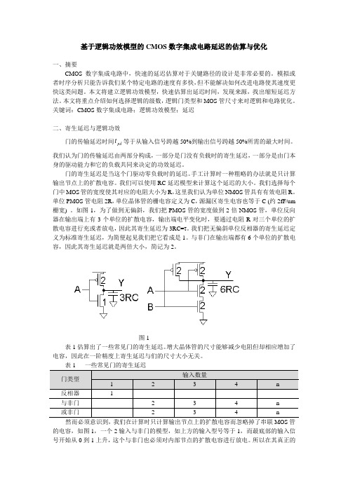
单位PMOS管电阻2R,单位晶体管的栅电容定义为C,源漏区寄生电容也等于C (约2fF/um 栅宽) 。
如图1,为了做到无偏斜,我们把PMOS管的宽度做到2倍NMOS管,单位反向器在输出端上有3个单位的扩散电容,输出端电平变化时,要通过电阻R对三个单位的扩散电容进行充或者放电,因此其寄生延迟为3RC=τ。
我们把无偏斜单位反相器的寄生延迟定义为标准寄生延迟,为简便起见我们把它看成是1。
与非门在输出端都有6个单位的扩散电容,因此其寄生延迟就是两倍大小,简记为2。
图1表1估算出了一些常见门的寄生延迟。
增大晶体管的尺寸能够减少电阻但却相应增加了电容,因此在一阶精度上寄生延迟与们的尺寸大小无关。
表1 一些常见门的寄生延迟的电容,如图1,一个2输入与非门的模型,如上方的输入型号等于1,而最底部的输入信号开始从0到1上升,这个与非门也必须对内部节点的扩散电容进行放电。
CMOS反相器

CMOS反相器由本书模拟部分已知,MOSFET有P沟道和N沟道两种,每种中又有耗尽型和增强型两类。
由N沟道和P沟道两种MOSFET组成的电路称为互补MOS或CMOS电路。
下图表示CMOS反相器电路,由两只增强型MOSFET组成,其中一个为N沟道结构,另一个为P沟道结构。
为了电路能正常工作,要求电源电压V DD大于两个管子的开启电压的绝对值之和,即V DD>(V TN+|V TP|) 。
1.工作原理首先考虑两种极限情况:当v I处于逻辑0时,相应的电压近似为0V;而当v I处于逻辑1时,相应的电压近似为V DD。
假设在两种情况下N沟道管T N为工作管P沟道管T P为负载管。
但是,由于电路是互补对称的,这种假设可以是任意的,相反的情况亦将导致相同的结果。
下图分析了当v I=V DD时的工作情况。
在TN的输出特性i D—v DS(v GSN =V DD)(注意v DSN=v O)上,叠加一条负载线,它是负载管T P在v SGP=0V 时的输出特性i D-v SD。
由于v SGP<V T(V TN=|V TP|=V T),负载曲线几乎是一条与横轴重合的水平线。
两条曲线的交点即工作点。
显然,这时的输出电压v OL≈0V(典型值<10mV ,而通过两管的电流接近于零。
这就是说,电路的功耗很小(微瓦量级)下图分析了另一种极限情况,此时对应于v I=0V。
此时工作管T N在v GSN =0的情况下运用,其输出特性i D-v DS几乎与横轴重合,负载曲线是负载管T P在v sGP=V DD时的输出特性i D-v DS。
由图可知,工作点决定了V O=V OH≈V DD;通过两器件的电流接近零值。
可见上述两种极限情况下的功耗都很低。
由此可知,基本CMOS反相器近似于一理想的逻辑单元,其输出电压接近于零或+V DD,而功耗几乎为零。
2.传输特性下图为CMOS反相器的传输特性图。
图中V DD=10V,V TN=|V TP|=V T= 2V。
【经典】CMOS非门中的传输时延分析
Contents•Defining “Delay” in a circuito Propagation delayo Transition timeo Practical input signals•“Rise-time” and “Fall-time”o Approximate Calculationo Inference from approximate calculationo Accurate calculations•Factors affecting propagation delay in CMOS inverterso Threshold Voltageo Width (W) of the MOSFETSo Supply voltageo Capacitive loado Short channel effectso Maximum operating frequency•The capacitance of CMOS inverters•ConclusionDefining “Delay” in a circuitEvery circuit has some parasitic capacitance components associated with it.In the chapter for non-ideal effects in MOSFETs, we have discussedthe parasitic capacitance present in the MOSFET device. These capacitance results in delaying the voltage change in the circuit. So we will getlimitations in our speed of operation depending on how fast we can charge or discharge these capacitors.To illustrate how the capacitances affect the output waveforms, we take some examples of waveforms. We will also define certain quantities such as “Propagation Delay” and “Transition Delay,” which will help us inquantifying the speed performance of our inverter.Propagation delayFigu Sup nex step the by aFigu“Pr In t by Theure 1: Cap ppose that xt stage cir p voltage aschematica load cap ure 2: Plotropagationthe plot of ande “hl” stan acitive load we have a rcuits. To t at the inpuc, we haveacitanceof the outp Delay.”f output vo. Here, thnds for high d connected a CMOS intest the spet, as shown represente .put voltageltage in fighe “p” in th h-to-low, ad to the outnverter wheed perform wn in the sced the cap e w.r.t. timegure 2, thehe subscrip and “lh” sttput termin hose outputmance of o chematic inacitance oe for a stepere are two pt stands fo tands for lonal of the C t is connecour circuitn figure 1.offered by t input signo time inter for propaga ow-to-high CMOS inve cted to somt, we applyNote thatthe next stal showingrvals markation delayh. The erterme y ain tageg the kedy.inv voltThe tim the tim thre outp the The Tr We tran corr Figu In t as “hl”tim erters in th tage is giv e propagat me required propagati me required eshold volt put voltag trip point e propagat ransitio e consider nsition tim responding ure 3: Plot the plot of and ”(“lh”) stame taken by he circuit a ven by tion delay d for the ou on delay f d for the ou tage value ge range. T is very clo tion delay n timea similar s me. For this g output cu of the outp f the output . The “t” i ands for higy output sig are operati , and the o for high to utput to fal for low to h utput to ris e used to de This definit ose to is then d situation fo s, we also c urve obtain put voltage t voltage, t n the subs gh-to-low(gnal to com ing betwee output low o low is giv ll fromhigh is giv se from efine the d tion fits wi .defined as or defining consider a ned is sho e w.r.t. time there are tw script stand (low-to-hime down f en two volt w voltage i ven byto ven by to delay time ith the CM the averag g another s a step input wn in figu e showing t wo time in ds here for gh). Thefrom 90% tages. The s given by and is def . and is defi . is at the m MOS invert ge ofa similar qua t voltage, t ure 3.the “Transi ntervals ma r transition is defineto 10% of e output hig y . fined as th Similarly fined as the Note that middle of th ter circuit and :antity calle the ition Time”arked n and ed by thefgh he y, e theheas ed ”the from In a thes Pr The take also the “raminpu m 10% to a similar m se two quaractical e input sig en as an ex o be driven input sign mp-signal”ut signal, w value. 90% of th manner the antities:input s nals to our xact step fu n by the ou nal to the in ” rather th we have p Similarly,etransition signalsr CMOS in function. B utput signa nverter we an a step slotted the is the value n time is de nverter in But, for pra al of some e are study signal. To input and time taken e. efined by t the previo actical scen other logi ying will b illustrate t output vol n by outpu taking the us discuss narios the ic gate. Th e more of the effect o ltage curve ut to rise up average of sions was inverter w his means t a of such an es in figure pf will that e 4.4: D Obs the star resu “R In t pro appbeg Delay in the serve from input sign rts to drop ults in the Rise-ti this section opagation d proximategin with ou e output pu m the figure nal goes be once the i output low ime” a n, we will delay dis derivationur mathem ulse due to e that the o elow the po input goes w pulse to and “F derive the scussed ea n and then wmatical deri a non-idea output sign oint below the be delayed Fall-tim e mathema arlier. First will do a fivations, th l input sign nal starts t . Simila e pointd w.r.t. the me”tical expre t, we will g formal derihere two im nalo climb up arly, the ou . This e input hig essions for go through ivation. Bumportant re Fig p once whe utput volta s ultimatel gh pulse. r the h anut, beforeesults that gureen agely we wewil circNot of t circ of t able this Her the of cAp In t pro loadto t fall ord Wh Thu inv l be using.cuits in lar • The ch flowin changethe cha te that this time . B cuit using t the instanta e to deduc s equation • For a c that the write th re the quan product o charging opproxim this section opagation d d attach the inverte l down to l der to get th hen we cro us, the PM erter circu . These res rge signal d hange in ch g through e in charge ange in vos formula i But, if we w this formu aneous cur ce the depe only.capacitor w e final stea he voltage ntity repr f the capac or discharg mate Ca n, we will delay of an hed to it. F r. Hence, t low value. he value fo oss the risin MOS transis uit formed sults are im domain. Th harge acro it times th e. This qua ltage acros is valid wh want to obt ula, then w rrent “I” in endence of with an init ady-state v e across the resents the citance and ging. alculatio do an appr n CMOS in For this pu the inverte This calcu or , we ng edge, th stor is obv is shown i mportant w hese are g ss a capac he time int antity is als ss the capa hen we are tain insigh we will use n the equat f delay on tial voltag value of th e capacitan e time con d the resis onroximate c nverter if w urpose, we er output w ulation wil will extrap hen the inp viously in c in figure 5when work iven by: itor is give erval over so equal to acitor. Mat e looking a hts on the w the averag tion. For m different p e across it e voltage a nce as a fu stant of th tance in se calculation we have a apply an i was initiall ll give us t polate the put to the c cut off reg .king with c en by the c which we o the capac thematical at a very sh working of ge current many cases parameters as and across it is unction of e circuit. eries with i n to figure capacitive ideal rising y high and the value o result.circuit is ion, so the capacitive current e see thecitance tim lly:hort interva f a capacit “<I>” inst s, we will s by solvin if we know s . We ca time to be is given b it at the tim out the eg edge inp d now it w of . In . e equivalen mes al tive tead be ng w an e:byme put will ntFigu of th At t to to its sgiv Thebelo Our from NM Tak curr We HerSim ure 5: Equ he outputthe instant . . Tsaturation en by:en, as the l ow r propagat m to MOS to be:king these rent as:e, will put t re, is g mplifying tivalent circ t of switch And also, This mean region. Thload capac . At thi tion delay . At th :two extrem this into th given bythe above e cuit of the C hing, the dr the gate-t s for the in hus the val citor dis s point, th is defined e point whme values he equationequations a CMOS inv rain-to-sou to-source v nstant the t lue of curr scharges, t he NMOS i by the tim here of the cur n:and solvin erter durin urce voltag voltage for transistor i rent suppli the drain-t is in linear me in which , we rrent, we ca ng forg ng high-to-l ge of NMO r the NMO is operatin ed by the i o-source v r region.h output fa e have the alculate thgives us: low transit OS is equa OS is equal ng in inverter is voltage fal alls current inhe average tion l llsn theHer Sim bec a faFiguof th The by:Her rep TheIn re, milarly, the cause in thi alling edgeure 6: Equhe outpute value obt re, is al lacing erefore, the ference • The pr the a in thersense ie results fo is case the e input is s ivalent circ tained for so a simila withe propagate from aropagation and valu e “on-stateintuitively,or will e NMOS w hown in fi cuit of the C propagatio ar quantity in the eq tion delay approxi delays areues. This m e” increase, as the ser depend on will be in cu figure 6.CMOS inv on delay foy, it’s value quation for of the circimate cae inversely means as the, the delay ries resista n the param ut-off. The erter durin or low to he can be ob r . cuit is givealculatiy proportio he conduc y time dec ance in the meters of th e equivalen ng low-to-h high transi btained by en by the a iononal totivity of th crease. Thi RC circui he PMOS,nt circuit f high transit ition is giv y average: he transisto is also mak it decrease , for tion ven ors keses,If w Ac In t We leve Fro ope We rela a co We HerSim the tim and dis • The va supply the delwe have• The de From a CMOS • The de Consid can say But, fo that ca power ccurate this section e will only el to high om , t erating in l e consider atively ver onstant cur e put this v re,mplifying t me constant scharging.alue of d y voltage. C lay values , thenelay time is a design po S inverter s elay time is dering that y that as or small de an be used.dissipatio calcula n, we will go over th level. For the PMOS linear regio that the PM ry short tim rrent sourc value of theand the equatiot also decr depends on Consider th for high-to n both the s directly p oint of view should be s inversely t the fact increase evices, ther Also, the n which w ationsderive a m he calculat this purpo transistor on.MOS trans me . If the ce. The cure current inons and sol reases. Thu n the value hat the o-low and delay time proportion w, the par aimed to b y proportio tor is not a es, the spee re is a upp increase i will be disc much more tions for th ose we will is in satur sistor stays e transisto rrent is giv n the equa lving for us, there is of the thre low-to-hig es are equa nal to the lo rasitic capa be kept at a onal to the a very stron ed of opera per bound t n supply v cussed in th e accurate he output t l consider ration and s in it’s sat or is in satu ven by:ation:, we get:s faster rate eshold vol . If, we wa gh transiti al. oad capaci acitances p a minimum supply vo ng function ation also to the supp voltage res he next po value for t ransition f two time i for ,turation re uration, the e of charg ltage andant to mat ions, then:itance . present in t m value. oltage .n of , wincreases.ply voltage sults in mo ost.the delay t from low intervals. , it is egion for a en it acts li ing ch the wee ore time. ikeThe valu curr We Thi fun diff Sup abo RH Sol volt Sim Her not proFinsup we Thefiguis m en, we wil ue ofrent is giv e put the va is gives us nction of tim ferential eq ppose that ove equatio HS =lve the abo tage runs f mplifying, re, exact but opagation d nally, we g ppose thatget: e rise in ouure 7. For marked as l solve for . In this r en by:alue ofan differe me “t”. W quation caon simplifiove equatio from we get:. We repl this will gdelay. et: utput volta linear regi r the timeregion the in the relaential equa We will notn be easily = u andies to: ons for “t” to .lace the va give us an i , then, p age when w , the PMion or “line takes t transistor ation given ation whichperform th y solved by” running f alue of idea of the putting the we apply a MOS transiear chargin to rise to is in saturan by: h can be so he calculat y the follo = a, th from to wi e effect of ese values i a negative e istor is in sng”. And f from ation mode olved to fin tions here,owing obse hen the RH . And the ith . T “on-resist in the abov edge input saturation. for the initial de, thus the nd as , but the ervations:HS of the e output The relatio tance” on t ve equatio t is shown This regio , the e aon istheonin onPM cha Figu cap The get The sho also satu thediscMOS enters arging”.ure 7: Plot pacitancee derivatio is given b e fall in ou own in figu o divided i uration and NMOS ischarge. s triode mo of output v on fori by: utput voltag ure 8. Simi into two re d this is min triode m ode, this is voltage w.r s analogou ge on the a ilar to the c egions. For arked as limode and s marked b r.t. time du us to the oapplication charging o r inear dischthis region by sublinea ring the ch ne we did n of a risin of capacita , t harge. Andn is marke ar region o harging pha above. Th ng edge inp ance, the di the NMOS d ford as sublin or “subline ase of the lo he result w put signal discharging S is innear ar oad weis g is,Figu the The app the If w that thre the Not take rela the onlythe Fa CM We varsomure 8: Plot load capac e readers a proximate “on-resist we plot the t the propa eshold volt speed of o te that the e into acco ationships,hand calc y proceed output of actors MOS e have earl ious factorme of the c of output v citanceare advised calculation tance” is in e above del agation del tages. The operation o hand calcu ount the no , one shoul ulations do with simu the circuit s affect invert ier discuss rs. In this sconsequenc voltage w.r d to check n also hold nversely pr lay values lays increa erefore hav of the circu ulations do on-ideal ef ld use the o provide ulations wh t.ting p terssed the dep section, wces from a r.t. the time that the in ds for the a roportiona w.r.t. the ase with th ving low th uit.one in this ffects of th different c a good am hen we hav propag pendence o we will suma design po e during th nference is accurate ca al to the threshold he rise in th hreshold v s section ar he MOSFE circuit sim mount of de ve some qu gation of the prop mmarise theoint of view e dischargi drawn in alculations or valu voltages, w he magnitu oltage valu re not exac ETs. For th ulators ava esign insig uantitative delay pagation d em and alsw. ing phase o the case o s. Note tha ues.we observ ude ofues improv ct. They do he exactailable. Bu ghts. We m e idea abou y in delay onso look ov of f at e ves on’t ut, must uterTh Wit also MO the in oW As the likekep mo impBut cap log in tSu The Thu the But be u volt Ca The man curr cap cap in b Sh hreshold th the decr o decrease OSFETs w body and order to rem Width (W we have s and ve to keep h pt equal for dulation e provement t, this incre pacitance in ic gate, the the degrada upply vo e propagat us increasi inverter.t, for smal used in ord tage result apacitiv e parasitic nifests as t rent stage pacitor()pacitances brief in the hort cha d Volta rease in th es. Thus, fo with very lo source ter move the b W) of the een that th values for higher valu r the devic ffect. Thus t in the spe ease in wid n the CMO en it will s ation in th oltagetion delay h ing the sup l devices, der to not d ts in the dy ve loadcapacitanc the capacit inverter an ). Thus, fo as low as p e next secti annel ef gee value of or faster ci ow thresho rminals are body effec e MOSF he propaga NMOS an ues of (W/L ces in orde s if we inc eed of oper dth also re OS inverte see a high e speed of has an inv pply voltag there is an damage th ynamic pow ce present tive load(nd the nex r better sp possible. T ion.ffectsf threshold ircuit opera old voltage e connecte ct. FETSation delay nd PMOS L). Genera er to have a crease the c ration. esults in an er. If this in capacitive f the overa verse relati ge will resu n upper lim he circuit. A wer consu t in the ove ). The p xt stage inv peed, we m This parasi voltage, th ation, we w es. This is w ed in both t y decreases respective ally, the ch a similar o channel w n increase nverter is d e load. Thi all circuit.on with th ult in an in mit to the su Also, an in umption to erall CMO arasitic ca verter is a c must keep th itic capaci he propaga would like why we ha the NMOS s as we inc ely. Thus, w hannel leng order of ch idth (W), w of the para driving som s will ultim he supply v ncrease in upply volt ncrease in increase. OS inverter apacitance cause of th he parasiti tance will ation delay e to choose ave seen th S and PMO creasewe would gth (L) is hannel leng we will ge asiticme next st mately resu voltage(the speed tage that c supply r circuit from both his load ic be discuss y e hat OS gth et an age ult ). of an h the sedAs the conpro We the hapThu The M Sup inv oveBut We use circ than Th Till stag und It sh the precapwe have s MOSFETnsidering id opagation d e are now a conductiv ppens due us, the satu erefore, the aximum pposed tha erter, we a er which wt, we gener e have a lot es multiple cuit is muc n .he cap l now, we ge with a s derstanding hould be c parasitic c sent in thepacitance th een in the T device. B deal IV ch delay cons aware that vity of the to velocity uration cur e propagat m opera at after opt achieve a m we can oper rally opera t of logic g e CMOS in ch more th pacitan have been simple cap g of the co clear by no capacitanc e wiring us hat constit previous t But, we hav haracteristi iderations channel le device. Bu y saturatio rrent will b tion delay ating fre imizing th minimum d rate the inv ate our dig gates casca nverters. Th an . So nce of n represent pacitive loa omponents ow that the ce in the M sed to conn tutes our fi that there a ve done al ics. One of is “veloci ength is ke ut, for shor n and not be lower th will be mo equency he values o delay of verter will gital circuit aded toget herefore th o we opera f CMO ting the cap ad (). In s that make e capacitiv MOSFETs a nect the de inal is s are a lot of l our calcu f the most ity saturati ept minimu rt channel due to cha han that in ore.yof the MOS . Then t l be: t around th ther, and e he cumula ate at a freq OS inv pacitive lo n this sectio e up this ca e load is ju and the cap evices toge shown in f f non-ideal ulations on important on.”um in orde device, th annel lengt n long chan SFETs in t the maximu he range ach of thes ative delay quency mu verters oad offered on, we wil apacitive l ust a mani pacitive el ether. Thefigure 9. al effects in nly t effects of er to increa he saturatio th modula nnel device the CMOS mum frequese logic ga of the wh uch lower sd by the ne ll try to ge load.festation o lementsdifferent nf ase on ation. es. S ency ateshole ext t an ofFigu cap We tran the dra capThe we circmo to nimp The is c cap conNot the of c cha ure 9: Com pacitances i e consider nsistors in capacitive in-to-bodypacitance o e circuit sh will make cuit. The lo del will no note that th portant par e capacitor connected t pacitors nstant volta te that the other way change in v ange is V dd .mponents of n the circu a circuit o the circuit e compone y capacitan of the load hown in th e some mo oad capaci ot be accur he wiring c rameter as rs , to constan such that age value.voltage ac y around w voltage is . f the load c uitf two CMO t, namely M ents shown nce(), w inverter(e figure is difications itance valu rate but wi capacitanc we scale d and are nt value. W t finally, o cross the c when we sw 2 V dd . But capacitor d OS inverte M1, M2, M n are due to wiring capa ). s quite com s to the mo ue that wil ill still giv ce that weh down our e easy to a We would li one of its te capacitor C witch the in for every ue to differ ers. There M3, M4. In o gate-to-d acitance(mplex to be odel in ord l be obtain e us enoug have ment ICs.analyse as o ike to shift erminals is C gd changes nverter. Th other capa rent parasit are a total n the circu drain capac ) and fin e solved by der to get a ned from th gh insights tioned beco one of ther ft thes connecte s from +V d herefore th acitor, the iticl of four uit schemat citance (nally input y hand. Th a simplerhis simplif s. One thin omes an re termina ed to a dd to -V dd o he magnitu magnitude tic, ),hus, fied ng als rude e ofFigu the So,par chaorig Thu Co In t inv delathe thatgate dela One with valu havaim ure 10: Sim load capacwe shift tallel with ange of vol ginal one. us, our fina onclus this chapte erter is qu ay in a CM circuit aff t the CMO es. Hence,ay caused e of the po h an increa ue will res ven’t discumed at undemplified par citancethe gate-to , as sholtage, the e Therefore al expressi sioner, we have uantified. W MOS inver fect the pro OS inverter , the delay by the CM oints we m ase in supp sult in mor ussed whyerstanding rasitic capa -drain cap own in figu equivalent , the new v ion for the e seen how We derived rter circuit opagationr forms thein an over MOS invertmentioned eply voltage re dynamic this is the g this kind acitors con pacitance in ure 10. In o t capacitan value of ga e load capa w the speed d the formu t. We also delay of a e building rall logic crters used.earlier thate. But, als c power di case. The of effects nnections in n the circu order to ta nce has a v ate-to-drai acitance be d performa ulae that d saw how d a CMOS inblocks forcircuit willt the speed o an increa issipation i next post only. We n the model uit and plac ke into acc alue twice in capacitoecomes:ance of a Cdefine the p different p nverter. Ke r different l also depe d of operati ase in supp in the circu in this CM will learn l to calcula ce them in count the e as that of ors is CMOS propagatio parameters eep in min types of lo end upon th tion increa ply voltage uit. WeMOS cours about the te nf the .on s in d ogic he ses e se isdifferent types of power consumption in a CMOS inverter and the factors that influence it.。
(整理)图题91是用两个555定时器接成的延时报警器当开关S断开...
9.1 图题9.1是用两个555定时器接成的延时报警器。
当开关S 断开后,经过一定的延迟时间后,扬声器开始发声。
如果在延迟时间内开关S 重新闭合,扬声器不会发出声音。
在图中给定参数下,试求延迟时间的具体数值和扬声器发出声音的频率。
图中G 1是CMOS 反相器,输出的高、低电平分别为V OH =12V ,V OL ≈0V 。
图题9.5解:1.工作原理:图题9.1由两级555电路构成,第一级是施密特触发器,第二级是多谐振荡器。
施密特触发器的输入由R 1、C 1充放电回路和开关S 控制,当S 闭合时,V C =0V ,施密特触发器输出高电平。
施密特触发器的输出经反相器去控制多谐振荡器的R D 端,当施密特触发器的输出为高电平时,R D =0,多谐振荡器复位,扬声器不会发出声音。
当开关S 断开后,R 1、C 1充放电回路开始充电,V C 随之上升,但在达到CC T 32V V =+之前,施密特触发器的输出仍为高电平时,R D =0,扬声器仍不会发出声音。
这一段时间即为延迟时间。
一旦V C 达到CC T 32V V =+,施密特触发器触发翻转,输出低电平,R D =1,多谐振荡器工作,扬声器开始发声报警。
2.求延迟时间:延迟时间由R 1、C 1充放电回路的充电过程决定:τtev v v v -+∞-+∞=)]()0([)(C C C C将 V 12)(CC C ==∞V v )0(C +v =0V τ=R 1C 1代入上式,得: )1(11CC C C R t eV v --=t=t 1时,CC C 32V v =代入上式,整理得延迟时间:t 1= R 1C 1ln3≈1.1 R 1C 1=1.1×10⁶+10×10-6=11S扬声器发声频率:MHz 95.01001.010157.01)2(7.0163232≈⨯⨯⨯⨯=+=-C R R f9.2图题9.2所示电路是由两个555定时器构成的频率可调而脉宽不变的方波发生器,试说明其工作原理;确定频率变化的范围和输出脉宽;解释二极管D 在电路中的作用。
CMOS反相器延迟时间
数字集成电路设计
实验报告
一、实验目的
通过实验了解CMOS反相器的工作原理,能自己用CMOS和PMOS 连接电路。
通过设置不同的measure参数表,求得上升延迟、下降延迟、高电平转低电平的延迟时间、低电平转高电平的延迟时间。
二、实验内容
1、用软件求出输入输出电压曲线
2、通过设置不同的参数求得上升延迟tr、下降延迟tf、高电平转低电平的延迟时间thl、低电平转高电平的延迟时间tlh。
三、实验原理
四、实验步骤
VTC曲线
最终求得上升延迟tr 、下降延迟tf 、高电平转低电平的延迟时间thl 、低电平转高电平的延迟时间tlh 。
五、实验心得
本次实验虽与上次实验相似,只是所求不一样。
通过改变参数,求得上升延迟tr、下降延迟tf、高电平转低电平的延迟时间thl、低电平转高电平的延迟时间tlh,使我进一步了解mos管延迟。
集成电路设计基础_华中科技大学中国大学mooc课后章节答案期末考试题库2023年
集成电路设计基础_华中科技大学中国大学mooc课后章节答案期末考试题库2023年1.画小信号等效电路时,恒定电流源视为。
答案:开路2.模拟集成电路设计中可使用小信号分析方法的是。
答案:增益3.模拟集成电路设计中可使用大信号分析方法的是()。
答案:输出摆幅4.题1-1-1 中国高端芯片联盟正式成立时间是:。
答案:2016年7月5.题1-1-2 如下不是集成电路产业特性的是:。
答案:低风险6.题1-1-3 摩尔定律是指集成电路上可容纳的晶体管数目,约每隔:个月便会增加一倍,性能也将提升一倍。
答案:187.MOS管的小信号模型中,体现沟长调制效应的参数是()。
答案:8.工作在饱和区的MOS管,可以被看作是一个。
答案:电压控制电流源9.下图中的MOS管工作在区(假定Vth=0.7V)。
【图片】答案:饱和区10.一个MOS管的本征增益表述错误的是。
答案:与MOS管电流无关11.工作在区的MOS管,其跨导是恒定值。
答案:饱和12.MOS管中相对最大的寄生电容是。
答案:栅极氧化层电容13.MOS管的小信号输出电阻【图片】是由MOS管的效应产生的。
答案:沟长调制14.题1-1-4 摩尔定律之后,集成电路发展有三条主线,以下不是集成电路发展主线的是:。
答案:SoC15.题1-1-5 单个芯片上集成约50万个器件,按照规模划分,该芯片为:。
答案:VLSI16.题1-1-6 年发明了世界上第一个点接触型晶体管。
答案:194717.题1-1-7 年发明了世界上第一块集成电路。
答案:195818.题1-1-8 FinFET等多种新结构器件的发明人是:。
答案:胡正明19.题1-1-9 集成电路代工产业的缔造者:。
答案:张忠谋20.题1-1-10 世界第一块集成电路发明者:。
答案:基尔比21.MOS管一旦出现现象,此时的MOS管将进入饱和区。
答案:夹断22.MOS管从不导通到导通过程中,最先出现的是。
答案:耗尽23.在CMOS模拟集成电路设计中,我们一般让MOS管工作在区。
数字集成电路学习总结5CMOS反相器
数字集成电路学习总结5CMOS反相器今天开始总结数字集成电路。
这本书其实算是本科最难的⼀本了,细节过多⽆法卒读,涉及到的知识也⾮常全⾯。
实际上本科课程安排中并为将其作为重点,我们的课⾮常⽔,不知道讲了什么。
今天详细总结⼀下。
当时然由于内容过多,⽆法全部涵盖,只能⼤致总结,并着重记录定性的结论。
涉及到计算之类的问题,就只能略过了。
第五章 COMS反相器5.1 引⾔为什么从第五章开始,原因是这章⽐较基础,详细学习CMOS反相器后,才能继续看组合电路和时序电路等等。
研究的对象有如下⼏个指标:成本(复杂性和⾯积)、完整性和稳定性(静态特性)、性能(动态特性)、能量效率(功耗)。
5.2 静态CMOS反相器——直观综述课本上的描述:晶体管只不过是⼀个具有⽆限关断电阻和有限导通电阻的开关。
以开关来理解,可以推导出其他重要特性:1、输出⾼电平和低电平分别为VDD和GND,换⾔之,电压摆幅等于电源电压。
因此噪声容限很⼤。
2、逻辑电平与器件的相对尺⼨⽆关,所以晶体管可以采⽤最⼩尺⼨。
这⾥有⼀个概念叫⽆⽐逻辑3、稳态时,输出和VDD或GND之间总存在有限电阻的通路。
因此⼀个设计良好的CMOS反相器具有低输出阻抗,这使得它对噪声和⼲扰不敏感。
4、输⼊电阻极⾼。
理论上,单个反相器可以驱动⽆穷个门,或者说有⽆穷⼤的扇出。
但很快我们发现增加扇出也会增加传播延时。
因此扇出不会影响稳态特性,会影响瞬态特性。
5、忽略漏电流的话,意味着⽆静态功耗。
之前常⽤的是NMOS电路,静态功耗不为0,限制了集成度。
后来必须转向CMOS。
电压传输特性(VTC)的性质和形状可以通过图解法迭加两管的图像得到。
结果是观察到VTC具有⾮常窄的过渡区。
我们可以把开关特性简化为RC电路,⼀个快速门的设计是通过减⼩输出电容或者减⼩晶体管的导通电阻(增⼤宽长⽐)实现的。
5.3 CMOS反相器稳定性的评估——静态特性5.3.1 开关阈值开关阈值VM定义是Vin=Vout的点,利⽤图解法可以看出。
- 1、下载文档前请自行甄别文档内容的完整性,平台不提供额外的编辑、内容补充、找答案等附加服务。
- 2、"仅部分预览"的文档,不可在线预览部分如存在完整性等问题,可反馈申请退款(可完整预览的文档不适用该条件!)。
- 3、如文档侵犯您的权益,请联系客服反馈,我们会尽快为您处理(人工客服工作时间:9:00-18:30)。
㊀山西电子技术2019年第2期应用实践㊀收稿日期:2018-11-11作者简介:崔建国(1969 ̄)ꎬ男ꎬ山西阳泉人ꎬ副教授ꎬ主要从事工业控制计算机在工农业生产实践中的应用ꎮ文章编号:1674 ̄4578(2019)02 ̄0003 ̄03基于cmos反相器的可精确计算延时电路崔建国ꎬ宁永香(山西工程技术学院ꎬ山西阳泉045000)摘㊀要::CMOS反相器的阈值电压为供电电压的一半ꎬ但有-15%~+15%合计30%的运行误差ꎬCMOS反相器之间阈值电压的个体差异ꎬ使工程师设计传统RC延时电路时ꎬ如果以UC=0.5VCC作为阈值电压设计延时㊁该电路实际运行所获得的延时与设计初衷之间的误差很大ꎬ设计参数不能拿来引用ꎮ设计一种可以精确计算的延时电路ꎬ电路仍以UC=0.5VCC作为阈值电压设计延时ꎬ这个延时电路采用了两个RC延时网络和两个反相器串联ꎬ每个RC网络产生相同的延时ꎬ两个CMOS反相器无论以哪一种有误差的阈值电压运行㊁最后获得的实际延时都与设计初衷相差无几ꎬ参数可以直接拿来引用ꎮ关键词:RC延时电路ꎻτꎻCMOS反相器ꎻ阈值电压ꎻ设计参数ꎻ运行误差中图分类号:TP271㊀㊀文献标识码:A0㊀引言在人们的日常生活或工农业电气设备控制方面ꎬ有众多场合都需要对电路进行延时开关ꎬ实现的方法有许多ꎬ可以用最简单的机械定时器实现定时或延时控制ꎬ也可以用较复杂的电脑通过编程实现ꎮ当然ꎬ最常用的实现的方法是采用阻容RC定时网络电路连接一个反相器实现ꎬ见图1ꎬ这种电路非常方便㊁非常实用ꎬ常常在一些电子或电气控制电路中见到ꎮ遗憾的是ꎬRC定时网络的每个元件数值均有明显的误差ꎬ以致不能事先精确地确定或计算延时的时间[1]ꎮ图1㊀一般延时器电气原理图这里我们采用两个RC网络和两个反相器ꎬ依次串联ꎬ形成一个新颖的定时或延时电路ꎬ这样可以明显地改进延时的精确度ꎮ1㊀一般延时器电路实际工作时获得的延时与设计初衷的差别㊀㊀图1是一个比较典型㊁比较简单的延时器电路ꎬ采用阻容RC定时网络电路连接一个反相器实现ꎬ反相器是可以将输入信号的相位反转180ʎ的电路ꎬ这种电路广泛应用在模拟电路中ꎬ比如音频放大ꎬ时钟振荡器等ꎮ在电子线路设计中ꎬ经常要用到反相器ꎮCMOS反相器电路由两个增强型MOS场效应管组成ꎮ而典型的TTL与非门电路由输入级㊁中间级㊁输出级组成ꎮ以常用的CMOS反相器电路为例ꎬ图1所示的CMOS反相器的阈值电压为供电电压的一半ꎬ即1/2VCCꎬ并有-15%~+15%合计30%的误差ꎮ其中τ是RC延时电路的时间常数ꎬτ=RCꎻαt可以认为30%的阈值误差电压所造成的延时或定时的误差[2]ꎮ图2示出了反相器电路的输入信号曲线ꎬ其中横轴为XꎬX=t/τꎬX为时间常数τ的倍数ꎬt为电容充电时间ꎻ纵轴为 1 ꎬ曲线代表函数1=e-Xꎮ按照上文所指出CMOS反相器的阈值电压可能有30%的误差ꎬ那么在图1所示的延时电路中ꎬ如果输入电压UC(电容C上的充电电压)为0.35VCC~0.65VCC之间的任何一个电压值ꎬ图1中反相器的输出都有可能出现逻辑 0 或逻辑 1 的状态ꎮ图2㊀CMOS反相器电路的输入信号曲线图至于输出是 0 还是 1 ꎬ在于电容属于充电过程还是放电过程ꎬ充电过程中UC电压值超过反相器的阈值电压(可能0.35VCC~0.65VCC之间的任何一个电压值)时ꎬ反相器输出 0 ꎻ电容放电过程中ꎬUC电压值低于反相器的阈值电压时ꎬ反相器输出高电平12V(假如反相器供电为12V)ꎮ从图2可以看出ꎬ这两种状态(0.35VCC以及0.65VCC)分别对应于电容通过电阻充电到0.43τ和1.05τ(τ=RC)的时间ꎮ因为CMOS反相器的阈值电压为供电电压的一半ꎬ故阈值电压UC=0.5VCC时ꎬ图2中对应的电容充电时间要在t=0.69τ后才出现ꎮ对上面的关键点总结一下ꎬ我们通常设计延时电路时ꎬ一般以UC=0.5VCC作为阈值电压来计算延时时间ꎬ即电容的充电时间t=0.69τ时ꎬ反相器输出电平开始反转ꎬ但由于CMOS反相器的阈值电压可能有30%的误差这种特性ꎬ最后实际运行所得到的延时时间有可能是UC(反相器输入电压)为0.35VCC~0.65VCC中的任意一点作为阈值电压时的时间[3]ꎮ所以在图1延时电路中ꎬ以UC=0.5VCC作为阈值电压设计延时所获得的时间与设计初衷之间的误差还是很大的ꎬ工程师设计的参数不能直接拿来引用ꎮ2㊀可精确计算的延时电路的分析设计一个延时电路ꎬ这个延时电路仍以UC=0.5VCC作为阈值电压设计延时ꎬ对应的电容充电时间t0.5VCC=0.69τꎮ经过反复验证ꎬ延时电路实际运行所得到的延时时间与设计初衷所计算的延时时间虽然不是完全一样ꎬ但它们之间的误差已经大大缩小ꎬ设计参数可以直接引用ꎮ这个延时电路采用了两个RC网络和两个反相器ꎬ如图3所示ꎬ图中的每个RC网络产生相同的延时ꎬ且都等于图1所示电路总延时值的一半ꎬ第一个RC延时电路的延时值t1=0.5∗X1∗τꎬ对照图2ꎬ其中X1∗τ为第一个反相器的有误差阈值电压对应的充电时间ꎻ第二个RC延时电路的延时值t2=0.5∗X2∗τꎬ仍对照图2ꎬ其中X2∗τ为第二个反相器的有误差阈值电压对应的充电时间ꎮ图3㊀可精确计算的延时电路1电气原理图故图3延时电路的总延时t可以用以下公式简单计算:t=t1+t2=(0.5∗X1∗τ)+(0.5∗X2∗τ).其中τ为RC延时电路的时间常数ꎬτ=RCꎻX1与X2皆为0.43~1.05之间的任意一个值ꎬX1或X2与τ的乘积就是各个反相器有误差的阈值电压所对应的充电时间ꎮ以上求总延时公式我们可以以任意组合来计算其实际延时时间ꎬ从而与以UC=0.5VCC作为阈值电压时的设计延时时间作比较ꎬ来验证我们设计的合理性ꎮ首先以第一种情况验证图3设计的合理性ꎬ即第一个延时网络中的反相器以-15%的阈值电压误差求其实际延时时间t1=0.5∗X1∗τ=0.5∗0.43∗τꎻ第二个延时网络中的反相器以+15%的阈值电压误差求其实际延时时间t2=0.5∗X2∗τ=0.5∗1.05∗τꎬ故实际总延时为t=(0.5∗0.43∗τ)+(0.5∗1.05∗τ)=0.74τ.由此可以看出ꎬ虽然设计延时时间0.69τ与实际延时时间0.74τ之间仍有差距ꎬ但已经很接近设计值0.69τꎮ第二种情况ꎬ如果第一个延时网络中反相器恰好阈值电压为0.5VCCꎬ第二个延时网络中反相器阈值电压也恰好为0.5VCCꎬ那么实际总延时为t=(0.5∗0.69∗τ)+(0.5∗0.69∗τ)=0.69τ.这种情况下的设计延时与实际延时恰好一样ꎮ第三种情况ꎬ如果第一个延时网络中反相器阈4山㊀西㊀电㊀子㊀技㊀术㊀㊀㊀㊀㊀㊀㊀㊀㊀㊀㊀㊀㊀2019年㊀值电压为0.65VCCꎬ第二个延时网络中反相器阈值电压也恰好为0.65VCCꎬ那么实际总延时为t=(0.5∗1.05∗τ)+(0.5∗1.05∗τ)=1.05τ.这是两个反相器阈值电压误差最大㊁情况最恶劣的一种组合ꎬ其设计延时0.69τ与实际总延时1.05τ相差还是蛮大的ꎮ但第三种情况是一种特例ꎬ通过大量任意阈值电压组合的比较ꎬ我们可以证明采用图3设计方案所得到的延时器ꎬ相比较图1的一般延时器ꎬ工程师设计的延时时间与延时电路实际运行所得到的延时时间虽然不能完全一模一样ꎬ但它们之间的误差已经大大缩小ꎬ可以认为图3的延时电路是可以被精确计算的ꎬ设计参数是可以拿来直接引用的ꎮ从以上的分析我们就可以明白图4所示的电路也可得到同样精确的总延时ꎮ图4的工作原理仍然利用两个反相器的阈值电压的误差不总是处于最恶劣的状况ꎬ仍然可以以两个反相器阈值电压的误差的任意组合来计算其实际延时时间ꎬ从而证明图4所示的电路也可得到同样精确的总延时ꎬ这里不再重复证明ꎮ图4㊀可精确计算的延时电路2电气原理图3㊀注意事项图3的延时电路要想获得满意的结果ꎬ还有一个注意事项ꎬ就是其中的反相器必须采用CMOS反相器ꎬ其主要原因在于只有CMOS门电路的阈值电压为供电电压的一半ꎬ而且他们的输出电压只能是 0 或 供电电压值 ꎬ这里是不能采用斯密特触发器的ꎬ因为斯密特触发器有两个阈值电压ꎬ且不一样[4]ꎮ若采用4000系列的CMOS电路ꎬ其延时时间太长的话ꎬ可采用74HCXX系列电路ꎬ74HCXX系列电路的引脚功能和L4LSXX系列兼容ꎮ4㊀结语本设计的延时电路采用两个RC网络和两个反相器串联ꎬ每个RC延时器得到的实际延时虽然与设计值仍有误差ꎬ但由于两个延时器其误差方向不可能总是相同ꎬ故它们的总延时与设计值相差并不大ꎬ有时甚至相同ꎮ这个电路设计虽然不能彻底解决误差的存在ꎬ但可以将误差尽可能缩小ꎮ本设计的不足是反相器必须采用CMOS门电路ꎬ斯密特触发器㊁TTL门电路不适合这种设计ꎮ参考文献[1]㊀韩广兴.电子元器件与实用电路基础[M].修订版.北京:电子工业出版社ꎬ2005.[2]㊀何晓燕ꎬ王庆春.CMOS反相器电压传输特性的分析和仿真[J].安康师专学报ꎬ2006(2):63-68.[3]㊀陆德纯.用一个CMOS反相器电路得到延迟和上升时间可控的脉冲[J].集成电路应用ꎬ1984(1):77.[4]㊀邵牟舟ꎬ秦世才ꎬ贾香鸾.MOS型反相器[J].半导体杂志ꎬ1995(3):5-8ꎬ13.AnAccurateTimeDelayCircuitBasedonCMOSInverterCuiJianguoꎬNingYongxiang(ShanxiEngineeringandTechnologyCollegeꎬYangquanShanxi045000ꎬChina)Abstract:ThethresholdvoltageoftheCMOSinverterishalfofthepowersupplyvoltageꎬbuttheoperatinger ̄rorofthe-15%~+15%whichistotalof30%andtheindividualdifferenceofthethresholdvoltagebetweentheCMOSinvertersmakethatwhentheengineersdesignthetraditionalRCdelaycircuitꎬifUC=0.5VCCisusedasthethresholdvoltagetodesignthedelayꎬthentheerrorbetweenthedelayobtainedbytheactualoperationofthecircuitandtheoriginalintentionofthedesignisverygreatꎬandthedesignparameterscannotbequoted.Atime-delaycircuitꎬwhichcanbeaccuratelycalculatedꎬisdesignedinthepaperbyUC=0.5VCCasathresholdvolt ̄age.ThedelaycircuitusestwoRCdelaynetworksandtwoinvertersinseries.EachRCnetworkproducesthesamedelayꎬnomatterwhichthresholdvoltagethetwocmosinvertersrunonꎬtheactualdelayobtainedintheendisal ̄mostthesameasthatoftheoriginaldesignꎬandtheparameterscanbedirectlyquoted.Keywords:RCdelaycircuitꎻτꎻCMOSinverterꎻthresholdvoltageꎻdesignparametersꎻoperationerror5㊀第2期㊀㊀㊀㊀㊀㊀㊀㊀㊀崔建国ꎬ等:基于cmos反相器的可精确计算延时电路。