5大规模数字集成电路习题解答
数字集成电路考题(2012)
集成电路考题一、填空题1、世界上第一个自动计算器是1832年。
2、Jack Kilby 提出IC 设想-—集成电路,由此获得诺贝尔奖,标志着数字时代的来临。
3、集成电路的发展按摩尔定律发展变化。
4、数字电路噪声进入的途径有电感耦合、电容耦合、电源和地的干扰。
5、N 型半导体的多子是自由电子,少子是空穴.6、P 型半导体的多子是空穴,少子是自由电子.7、二极管电流D I 与电压D V 的关系表达式为)1(/-=ΦT D V S D e I I 。
8、二极管的反向击穿类型有齐纳击穿和雪崩击穿。
9、互连线电容模型可用平行板电容模型等效,导线总电容的公式为10、互连线电容模型可用微带线模型等效,由平面电容和边缘电容构成。
11、导体为均匀的绝缘介质包围,可知一条导线的电容C 与电感L 的关系为u CL ε=。
12、CMOS 反相器噪声容限的定义有L NM 低电平噪声容限和H NM 高电平噪声容限.13、CMOS 反相器电路总功耗分为三部分,分别为dyn P 由充放电电容引起的动态功耗、dp P 直流通路电容引起的功耗、stat P 静态功耗。
14、静态CMOS 门由上拉网络PUN 和下拉网络PDN 构成。
15、CMOS 互补逻辑实现一个N 输入逻辑门所需MOS 管的个数为2N 个。
16、伪NMOS 逻辑实现一个N 输入逻辑门所需MOS 管的个数为N+1个。
17、动态逻辑实现一个N 输入逻辑门所需MOS 管的个数为N+2个。
18、动态逻辑电路工作过程分为预充电和求值两个阶段。
19、时序电路中与寄存器有关的参数分别为建立时间、维持时间、传播时间。
20、对于时钟偏差不敏感的触发器为Clocked CMOS (或为时钟控制CMOS )。
21、2C CMOS 实现一个N 输入逻辑门所需MOS 管的个数为N+2个。
2223、半定制的电路设计方法分别是以单元为基础的设计方法和以阵列为基础的设计方法。
二、简答题1、画出双阱CMOS电路工艺顺序简化图.(P31)2、二极管的电流受工作温度的双重影响。
数字集成电路习题答案

W / L 1 根据VGS和VDS确定其处于线性、饱和还是截止状态,并求 I D
的值。
解: (1)nm os:
VGT VGS VT 0 2.5 0.43 2.07 VDS
nm os 处于饱和区 ,Vmin VGT 2.07
2 W V ' I D kn ( )(VGT Vmin min )(1 VDS ) L 2 2 2 . 07 115 (2.072 )(1 0.06 2.5) 2 283.3A
VT0(V)
NMOS PMOS 0.43 -0.4
(V0.5)
0.4 -0.4
VDSAT(V)
0.63 -1
k’(A/V2)
115×10-6 -30×10-6
(V-1)
0.06 -0.1
1.假设设计一个通用0.25m CMOS工艺的反相器,其中PMOS晶体管的 最小尺寸为(W=0.75m,L=0.25m,即W/L=0.75/0.25) , NMOS晶体管 的最小尺寸为(W=0.375m,L=0.25m,即W/L=0.375/0.25) 求出g,VIL,VIH,NML,NMH
( R1 R2 R5 )C5
DCLK 3 R1C1 R1C2 ( R1 R3 )C3 R1C4 R1C5
(b)
DCLK 1 R1C1 ( R1 R2 )C2 R1C3 ( R1 R2 R4 )C4 ( R1 R2 )C5
9 RC
DCLK 2 R1C1 ( R1 R2 )C2 R1C3 ( R1 R2 )C4
( R1 R2 R5 )C5 9 RC
DCLK 3 R1C1 R1C2 ( R1 R3 )C3 R1C4 R1C5
数字集成电路习题
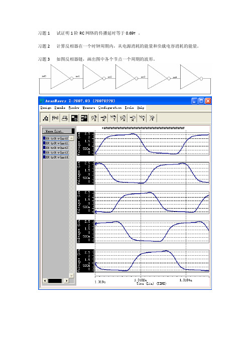
带入延迟公式可得,反相器链的延迟
t p N t p 0 (1
N
F
) 5 70 ps (1
5
2000 ) 1960 ps 2ns 1
c. 方法 a 的延迟时间
t p t p 0 (1
j 1
N
C g , j 1
C g , j
) t p 0 (1
解:VGS=VDS=2.5V,管子工作在饱和区。 栅沟电容 CGC=W*L*Cox=0.36um*0.24um*6fF/um2=0.52fF 栅与源漏区的交叠电容 Cov=CGSO=CGDO=W*Co=0.36um*0.31fF/um=0.11fF 栅电容 CG=CGC+2Cov=0.52 fF +2*0.11 fF=0.74fF 栅源电容 CGS=2CGC/3+Cov=2*0.52fF/3+0.11=0.46fF 栅漏电容 CGD=Cov=0.11fF 管子的源区和衬底都接地,所以源衬底扩散结处于零偏状态。有 Cs,bottom=W*LD*Cj0=0.36um*0.625um*2fF/um2=0.45fF Cs,sw=(W+2LD)*Cjsw0=(0.36um+2*0.625um)*0.28um/fF=0.45fF CSB= Cs,bottom + Cs,sw =0.45fF+0.45fF=0.9fF 管子的漏区接 2.5V,衬底接地,所以漏衬底扩散结处于反偏状态。有 CD,bottom=W*LD*Cj0/(1-VD/φ b)mj =0.36um*0.625um*2(fF/um2)/[1-(-2.5V)/0.9V]0.5 =0.23fF CD,sw=(W+2LD)*Cjsw0/(1-VD/φ bsw)mjsw =(0.36um+2*0.625um)*0.28(um/fF)/[1-(-2.5V)/0.9]0.44 =0.25fF CDB= CD,bottom + CD,sw =0.23fF+0.25fF=0.48fF
超大规模集成电路设计导论考试题及答案

1、MOS集成电路的加工包括哪些基本工艺?各有哪些方法和工序?答:(1)热氧化工艺:包括干氧化法和湿氧化法;(2)扩散工艺:包括扩散法和离子注入法;(3)淀积工艺:化学淀积方法:1 外延生长法;2 热CVD法;3 等离子CVD 法;物理淀积方法:1 溅射法;2 真空蒸发法(4)光刻工艺:工序包括:1 涂光刻胶;2 预烘干;3 掩膜对准;4 曝光;5 显影;6 后烘干;7 腐蚀;8 去胶。
2、简述光刻工艺过程及作用。
答:(1)涂光刻胶:为了增加光刻胶和硅片之间的粘附性,防止显影时光刻胶的脱落,以及防止湿法腐蚀产生侧向腐蚀;(2)预烘干:以便除去光刻胶中的溶剂;(3)掩膜对准:以保证掩模板上的图形与硅片上已加工的各层图形套准;(4)曝光:使光刻胶获得与掩模图形相同的感光图片;(5)显影:将曝光后的硅片浸泡在显影液中,使正光刻胶的曝光部分和负光刻胶的未曝光部分被溶解掉;(6)后烘干:使残留在光刻胶中的有机溶剂完全挥发掉,提高光刻胶和硅片的粘接性及光刻胶的耐腐蚀性;(7)腐蚀:以复制在光刻胶上图形作为掩膜,对下层材料进行腐蚀,将图形复制到下层材料中;(8)去胶:除去光刻胶。
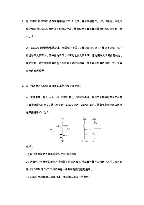
3、说明MOS晶体管的工作原理答:MOS晶体管有四种工作状态:(1)截止状态:即源漏之间不加电压时,沟道各电场强度相等,沟道厚度均匀,S、D之间没有电流I ds=0;(2)线性工作状态:漏源之间加电压Vds时,漏端接正,源端接负,沟道厚度不再均匀,在D端电位升为V d,栅漏极电位差为Vgs-Vtn,电场强度变弱,反型层变薄,并在沟道上产生由D到S的电场E ds,使得多数载流子由S端流向D端形成电流I ds,它与V ds变化呈线性关系:I ds=βn[(V gs-V tn)-V ds/2]V ds(3)饱和工作状态:Vs继续增大到V gs-V tn时,D端栅极与衬底不足以形成反型层,出现沟道夹断,电子运动到夹断点V gs-V ds=V tn时,便进入耗尽区,在漂移作用下,电子被漏极高电位吸引过去,便形成饱和电流,沟道夹断后,(V gs-V tn)不变,I ds 也不变,即MOS工作进入饱和状态,I ds=V gs-V tn/R c(4)击穿状态:当Vds增加到一定极限时,由于电压过高,晶体管D端得PN结发生雪崩击穿,电流急剧增加,晶体管不能正常工作。
习题数电参考答案(终)

习题数电参考答案(终)第⼀章数字逻辑概论1.1 数字电路与数制信号1.1.1 试以表1.1.1所列的数字集成电路的分类为依据,指出下列IC器件属于何种集成度器件:(1)微处理器;(2)计数器;(3)加法器;(4)逻辑门;(5)4兆位存储器。
解:依照表1.1.1所⽰的分类,所列的五种器件:(1)、(5)属于⼤规模;(2)、(3)属于中规模;(4)属于⼩规模。
1.1.2⼀数字信号波形如图题1.1.2所⽰,试问该波形所代表的⼆进制数是什么?解:图题1.1.2所⽰的数字信号波形的左边为最⾼位(MSB),右边为最低位(LSB),低电平表⽰0,⾼电平表⽰1。
该波形所代表的⼆进制数为010110100。
1.1.3 试绘出下列⼆进制数的数字波形,设逻辑1的电压为5V,逻辑0的电压为0V。
(1)001100110011(2)0111010 (3)1111011101解:⽤低电平表⽰0,⾼电平表⽰1,左边为最⾼位,右边为最低位,题中所给的3个⼆进制数字的波形分别如图题1.1.3(a)、(b)、(c)所⽰,其中低电平为0V,⾼电平为5V。
1.1.4⼀周期性数字波形如图1.1.4所⽰,试计算:(1)周期;(2)频率;(3)占空⽐。
解:因为图题1.1.4所⽰为周期性数字波,所以两个相邻的上升沿之间持续的时间为周期,T=10ms。
频率为周期的倒数,f=1/T=1/0.01s=100Hz。
占空⽐为⾼电平脉冲宽度与周期的百分⽐,q=1ms/10ms×100%=10%。
1.2 数制1.2.1 ⼀数字波形如图1.2.1所⽰,时钟频率为4kHz,试确定:(1)它所表⽰的⼆进制数;(2)串⾏⽅式传送8位数据所需要的时间;(3)以8位并⾏⽅式传送的数据时需要的时间。
解:该波形所代表的⼆进制数为00101100。
时钟周期T=1/f=1/4kHz=0.25ms。
串⾏⽅式传送数据时,每个时钟周期传送1位数据,因此,传送8位数据所需要的时间t=0.25ms×8=2ms。
数字集成电路设计与系统分析答案

懂得1、Please illustrate the meaning of its voltage transfer characteristic to a logic gate, and describe the static behaviors showed in the voltage transfer characteristic curves.The electrical function of a gate is best expressed by its voltage transfer characteristic (VTC),which plots the output voltage as a function of the input voltage Vout=f(Vin).The high and low nominal voltage Voh and Vol;The gate or switching threshold voltage Vm,that is define as Vm=f(Vm)(The gate threshold voltage presents the midpoint of the switching characteristics,which is obtained when the output of a gate is short circuited to the input);The high and low input voltage Vih and Vil are defined by the point where the gain (=dVout/dVin)of the VTC equals -12、Please draw the voltage transfer characteristic curve of the inverter and label the static operation points in the VTC.3、Please describe the definition of noise margin and its physical significance(物理意义), then draw the figure of definition of noise margins.The noise margins represent the levels of noise that can be sustained(所允许的) when gates are cascaded. A measure of the sensitivity of a gate to noise is given by the noise margins NML(noise margin low) and NMH(noise margin high), which quantize the size of the legal “0” and “1”, respectively, and set a fixed maximum threshold on the noise value4、Please describe the meaning of the regenerative property and the conditions of a gate with regenerative property.A gate with regenerative property ensures that a disturbed signal converges back to a nominal voltage level after passing through a number of logical stages. The VTC should have a transient region (or undefined region) with a gain greater than 1 in absolute value, bordered by the two legal zones, where the gain should be less than 1 in absolute value5、What are the definitions of the fan-out and fan-in properties?The number that can be driven is termed the fan-out of circuit, that denotes the number of load gates N that are connected to the output of the driving gate. The fan-in of a gate is defined as the number of independent input nodes to the gate.6、How to describe the performance of a digital IC? Please illustrate the parameters used to characterize the transient performance of a logic family, and draw the associated figure of the definition of these parP ropagation delay time and rise/fall time can be used to characterize the transient performance of a logic family .Propagation delay time of a gate expresses the delay experienced by a signal when passing through a gate,which represent how quickly the gate responds to the changes at its inputs.Rise/fall time express how fast a signal transits between the different levels. Propagation delay time is defined as the period between the 50%transition points of the input and output signals.Rise/fall time is defined as the period between the 10% and 90% points of the total voltage transition at the output waveforms.1、Illustrate the basic structure and simple operation principle of MOS transistor.Four terminals:source, drain, gate, body; Vertical Structure: gate electrode, insulator, semiconductor substrate; Horizontal Structure: source region, channel region, drain region2、Illustrate the basic function of each terminal of MOS device, and describe the general terminal connections of NMOS and PMOS transistor, respectively.The source and the drain are the electrodes conducting the current. The gate electrode is thecontrolling terminal. The function of the body is secondaryIn NMOS devices, the source is defined as the n+ region which has a lower potential(电势) than the other n+ region, the drain. The source is the terminal with the higher potential in PMOS devices, The body is generally connected to a DC supply that is identical for all devices of the same type (GND for NMOS, VDD for PMOS).3、What does the transition (or input) characteristic of MOS transistor mean? And what conclusions we can find from the characteristic curve?It describes the relationship between the gate-source voltage and the drain-source current with the certain drain-source voltage .When the gate-source voltage is less than the threshold voltage, the conducting current is zero, that is, the NMOS transistor is in cutoff operation. When is larger than, the NMOS transistor is on.4、What does the current-voltage (or output) characteristic of MOS transistor mean? And what conclusions we can find from the I-V characteristic curve?.It describes the relationship between the drain-source voltage and the drain-source current with a certain gate-source voltageVgs > Vt , 0<VDS <VGS -VT : Linear modeThe inversion layer forms a continuous current path between the source and the drain.A drain current proportional to Vds will flow from the drain to the source through the conducting channel. The channel region acts as a voltage-controlled linear resister.5、Describe the operation modes of NMOS and PMOS transistors respectively, and define the corresponding ideal current equations.1、Explain the channel-length modulation, sub-threshold conduction, short-channel effect and narrow-channel effect. And illustrate their corresponding chief impacts on the device.This simple current equation prescribes a linear drain-bias dependence for the current in MOS transistors, determined by the empirical model parameter λ, called the channel-length modulation coefficientOne typical condition, which is due to the two-dimensional nature of channel current flow, is the sub-threshold conduction in small-geometry MOS transistors.As a working definition, a MOS transistor is called a short-channel device if its channel length is on the same order of magnitude as the depletion region thicknesses of the source and drain junctions.The short-channel effects that arise in this case are attributed to two physical phenomena: the limitations imposed on electron drift characteristics in the channel; the modification of the threshold voltage due to the shortening channel lengthMOS transistor that have channel widths on the same order of magnitude as the maxium depletion region thickness are defined as narrow channel devices.For MOSFET with small channel widths,the actual threshold voltage increases as a result of this extra depletion charge of the fringe depletion region.This fact is called narrow channel effect.2、Describe the three main components of the load capacitanceCL, when a logic gate is driving other fan-out gates. And sketch the capacitance model of NMOS transistor.Gate capacitances (of other inputs connected to out)Diffusion(or junction) capacitances (of drain/source regions)Routing capacitances (output to other inputs)1,Describe the basic structure and operation of a static CMOS inverter. Then draw theassociated transistor schematicThis structure consists of an enhancement-type NMOS transistor and an enhancement-type PMOS transistor, operating in complementary mode. So this configuration is called Complementary MOS (CMOS). The gate terminals of the PMOS and NMOS transistors are connected to form the inverter input. The drain terminals of the PMOS and NMOS transistors are connected to form the inverter output. The source and the substrate of the NMOS transistor are connected to the ground, while the source and body of PMOS transistor are connected to VDD The circuit topology is complementary push-pull in the sense that: For high input the NMOS transistor drives (pulls down) the output node while the PMOS transistor acts as the load, and for low input the PMOS transistor drives (pulls up) the output node while the NMOS transistor acts as the load.When the input is at VDD: The NMOS is on (conducting) while the PMOS is off (cut-off). A direct path exists between Vout and the ground node, resulting in a steady-state value of 0V at the output. When the input is at ground:The NMOS is off while the PMOS is on. A direct path exists between VDD and Vout, yielding a high output voltage (equal to VDD).Static CMOS logic:structure:The static CMOS style is really an extension of the static CMOS inverter to multiple inputs. A logic function in static CMOS must be implemented in both NMOS and PMOS transistors. It is the combination of the pull-up network(PUN) and the pull-down network(PDN). Each input always connects to PUN and PDN simultaneously. The function of the PUN is to provide a connection between the output and VDD anytime the output of the logic gate is meant to be 1 (based on the inputs). The function of the PDN is to connect the output to VSS when the output of the logic gate is meant to be 0.Opreation: The pull-down net should be “on” when the pull-up net is “off” and vice versa. For any given input combination, the output is connected either to VDD or to ground via a low-resistance path. A DC current path between the VDD and ground is not established for any of the input combinations. With the complementary nature of NMOS and PMOS, the pull-up or the pull-down is “on” alternately to implement the logic operation.Discuss the main problems for high fan-in static CMOS gates and the associated techniques for fast complex gates.tpHL = 0.69 Reqn(C1+2C2+3C3+4CL); Propagation delay deteriorates(恶化) rapidly as a function of fan-in quadratically in the worst case, Gates with a fan-in greater than 4 become excessively slow and must be avoided.tPLH increases linearly due to the linearly increasing value of the diffusion capacitance;tPHL increase quadratically due to the simultaneous increase the resistance and internal capacitance in serial part.Transistor sizing: as long as fan-out capacitance dominatesProgressive transistor sizing: This approach reduces the dominant resistance, while keeping the increase in capacitance within boundsTransfer gate:Configuration:The source and drain nodes serve as inputs and outputs, while the gate node serves as the control input, the body node is connected to the power/ground Operation: For NMOS transfer gate,it turns on while the gate control terminal goes high, and the input signal will be delivered to the output node; it turns off while the gate control terminal goes low, and the output node will be impedance.CMOS transmission gate:Configuration: The CMOS transmission gate consists of one NMOS and one PMOS transistor, with the source and drain connected in parallel; The gate voltages appliedto these two transistors are also set to be complementary signals. The substrate terminal of the NMOS transistor is connected to ground and the substrate terminal of the PMOS transistor is connected to Vdd.Operation: If the control signal C is logic-high (equal to Vdd), then both transistors are turned on and provide a low-resistance current path between the input and output nodes. If the control signal C is logic-low, then both transistors will be off, and the path between the input and output nodes will be in the high-impedance state. The weakness of one device is overcome by the strength of the other device, whether the output is transmitting a high or low value. This is a clear advantage of the CMOS transfer gate over the single transistor counterpart.DCVLS:Operation: Assume now that, for a given set of inputs, PDN1 conducts while PDN2 does not, and that Out and out are initially high and low, respectively. Turning on PDN1: Causes Out to be pulled down (below VDD−|VTP |); Out is in a high impedance state, as M2 and PDN2 are both turned off. At the point M2 turns on and starts charging out非to VDD — eventually turning off M1; This in turn enables Out to discharge all the way to GND.XOR/XNOR: When the signals A and B have the same values, there is one conducting path either AB or A非B非; Then the output F is pulled down;At the same time, the other pull-down paths connected to the F非are both turned off. When F is pulled down below VDD−|VTP |, M2 t urns on and starts charging F非to VDD —eventually turning off M1 and pulling down F to Gnd. When the signals A and B have the different values, there is one conducting path either AB非or A非B; Then the output F非is pulled down; At the same time, the other pull-down paths connected to the F are both turned off. When F非is pulled down below VDD−|VTP |, M1 turns on and starts charging F to VDD —eventually turning off M2 and pulling down F非to Gnd.Precharge-Evaluate dynamic CMOS:Operation: Precharge (when the clock signal Φ= 0):The PMOS precharge transistor MP is conducting while the complementary NMOS transistor MN is off. The output load capacitance is precharged to VDD by MP, then VOH=VDD;The input voltages have no influence yet upon the output level since the complementary NMOS transistor MN is off. Evaluate (when the clock signal Φ=1):The precharge transistor MP turns off while the NMOS evaluate transistor MN turns on. The output node voltage may now remain at the logic-high level or drop to a logic low, depending on the input voltage levels: If the input signals create a conducting path between the output node and the ground, PDN is on, and the output capacitance will discharge toward VOL=0;Otherwise, when PDN is off, the output voltage remains at VOH= VDD.Domino dynamic CMOS logic:When Φ=0, during precharge: The output of the n-type dynamic gate is charged up to VDD, and the output of the inverter is set to 0. When Φ=1, during evaluation: The dynamic gate conditionally discharges, and there are two possibilities: The output node of the dynamic CMOS stage is either discharged to a low level through the NMOS circuitry (1 to 0 transition), or it remains high. Consequently, the inverter output voltage can also make at most one transition during the evaluation phase, from 0 to 1.TSPC dynamic CMOS logic:Configuration:If one constrains a NORA stage to have only n-precharge gates, and not static gates, then a p-channel transistor can be eliminated from the clocked latch; The dynamic circuit technique to be presented in that it uses only one-phase clock signal, so no clock skew problem exists. The NORA design style can be simplified so that a single clock is sufficient. For the doubled n-C2MOS latch, when φ= 1, the latch is in the transparent evaluate mode and corresponds to 2 cascaded inverters (non-inverting); For the doubled n-C2MOS latch, when φ= 0, both inverters are disabled (hold mode) -- only the pull-up network is still active.Pipelined NORA dynamic CMOS system:Configuration: Consists of an np-CMOS logic sequence and a clocked CMOS output buffer; A pipelined system can be constructed by simply cascading alternating φ-section and φ -section, meaning that evaluation occurs during active φ and φ respectively;Operation:φ=0, during hold mode :N block performs the precharge operation and pulls node Out1 up to VDD through the p-type device Mp1, while p block performs the discharge operation and pulls the node Out2 down to zero through the n-type device Mn2; The clocked CMOS latch will not be in operation and the previous output voltage will be stored on the output load capacitor CL. φ=1, during evaluate mode:All cascaded NMOS and PMOS blocks evaluate output levels one after the other, and then the signal Out2 will be inversed to the output node by the clocked CMOS latch in operation;Operation Mode: Evaluate―Hold: All logic stages perform the precharge-discharge operation when the clock is high, and all stages evaluate output levels when the clock is low. Therefore, wewill call this circuit a section, meaning that evaluation occurs during active .Clocked CMOS dynamic circuit:Basic Structure:A pair of PMOS and NMOS transistors controlled by the complementary clock signals are cascaded in the pullup and pulldown paths of the static CMOS gate, respectively, then a CMOS logic gate can be synchronized with a clock. Operation: φ=1, during evaluation mode:The transistors Mp1 and Mp2 are both turned on, then this gate can evaluate normally as a CMOS inverter to generate the logic output In非; φ=0 , during hold mode: Both transistors Mp1 and Mp2 are off, decoupling the output from the input. The CMOS circuit cannot conduct and evaluate, then the output Q retains its previous value stored on the output capacitor CL.Sequential logic:Virtually all useful systems require storage of state information, leading to another class of circuits called sequential logic circuits. In these circuits, the output not only depends upon the current values of the inputs, but also upon preceding output values. In other words, a sequential circuit remembers some of the past history of the system; A sequential circuit consists of a combinational circuit and a memory block in the feedback loop.Combination logic:In all logic circuits described so far, the output is directly related to the input. Typically, there are no feedback loops between the output and the input in these circuits (also classified as non-regenerative circuits), so the outputs are always a logical combination of the inputs. As a class, these circuits are known as combinational logic circuits. Combinational logic circuits, described earlier, have the property that the output of a logic block is only a function of the current input values, assuming that enough time has elapsed for the logic gates to settle. Static storage:preserve state as long as the power is on;are built using positive feedback or regeneration with an intentional connection between the output and the input;useful when updates are infrequent (clock gating)Dynamic storage:store state on parasitic capacitors;only hold state for short periods of time (milliseconds);require periodic refresh to annihilate charge leakage;usually simpler, so higher speed and lower power;useful in datapath circuits that require high performance levels and are periodically clockedLatch: level sensitive circuit that passes inputs to Q when the clock is high (or low);input sampledon the falling edge of the clock is held stable when clock is low (or high)Register or Flip-flops (edge-triggered): edge sensitive circuits that only sample the inputs on a clock transitionpositive edge-triggered: 0- 1negative edge-triggered: 1 -0built using latches (e.g., master-slave flip-flops)。
超大规模集成电路答案
⎞ ⎟⎠
(1
+
λnVM
)
= 115×10−6 × 2× 0.63× (1.05 − 0.4 − 0.63 / 2)(1+ 0.06×1.05)
= 52 ×10−6 A
g = − k Vn DSATn + k Vp DSATp
ID
(VM
)(λn
−
λ p
)
= − 1 2 ×115×10−6 × 0.63 + 3× 30×10−6 ×1
A:Al1 导线平面电容:(0.1×103μm2) ×30aF/μm2=3pF Al1 导线边缘电容:2×(0.1×106μm) ×40aF/μm=8pF Al1 导线总电容:CW=11pF Al1 导线电阻:RW=0.075Ω/□×(0.1×106μm)/ (1μm)=7.5kΩ Al1 导线的 r 和 c 值:c=110aF/μm;r=0.075Ω/μm
由VD2 > VDSATn ,确定 M2 发生速度饱和,因此
ID
=
kn
⎛ ⎜⎝ (VGS 2
− VT 2 )VDSAT
2
− VDSAT 2
⎞ ⎟⎠
,
VGS 2
= VT 2
+
⎛ ⎜ ⎝
ID kn
2
+ VDSAT 2
VDSAT
⎞ ⎟ ⎠
,
VGS 2
=
0.94
+
⎛ ⎜⎝
பைடு நூலகம்
0.2 ×10⁻³ 3× 8.9 ×10−5
( ) ID
=
kn 2
VGS 2 − VT 2
2 , VGS 2 = VT 2 +
2ID kn
大规模集成电路习题与答案
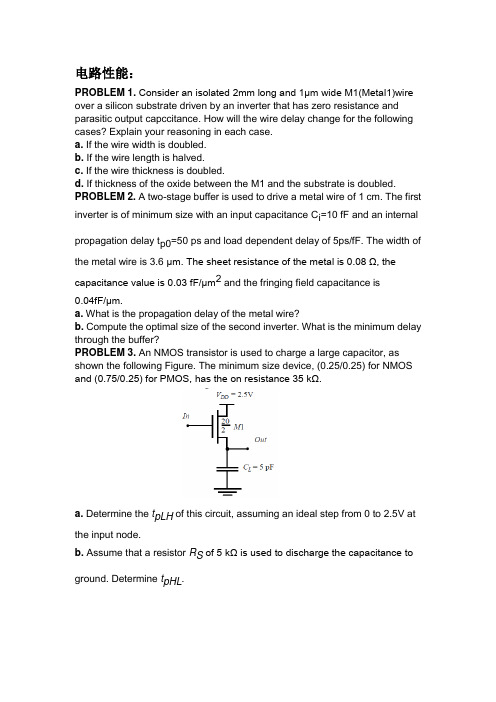
电路性能:PROBLEM 1. Consider an isolated 2mm long and 1μm wide M1(Metal1)wire over a silicon substrate driven by an inverter that has zero resistance and parasitic output capccitance. How will the wire delay change for the following cases? Explain your reasoning in each case.a. If the wire width is doubled.b. If the wire length is halved.c. If the wire thickness is doubled.d. If thickness of the oxide between the M1 and the substrate is doubled. PROBLEM 2. A two-stage buffer is used to drive a metal wire of 1 cm. The first inverter is of minimum size with an input capacitance C i=10 fF and an internalpropagation delay t p0=50 ps and load dependent delay of 5ps/fF. The width of the metal wire is 3.6 μm. The sheet resistance of the metal is 0.08 Ω, the capacitance value is 0.03 fF/μm2 and the fringing field capacitance is0.04fF/μm.a. What is the propagation delay of the metal wire?b. Compute the optimal size of the second inverter. What is the minimum delay through the buffer?PROBLEM 3. An NMOS transistor is used to charge a large capacitor, as shown the following Figure. The minimum size device, (0.25/0.25) for NMOS and (0.75/0.25) for PMOS, has the on resistance 35 kΩ.a. Determine the t pLH of this circuit, assuming an ideal step from 0 to 2.5V at the input node.b. Assume that a resistor R S of 5 kΩ is used to discharge the capacitance toground. Determine t pHL.c. The NMOS transistor is replaced by a PMOS device, sized so that k p is equal to the k n of the original NMOS. Will the resulting structure be faster? Explain why or why not.PROBLEM 4.The figure below assembles a RTL circuit where the active device is a NMOS transistor which has a resistive load. Assume the switch model behavior of the NMOS transistor. When V in <1.25V, the resistance of the transistor is infinite. When V in ≥1.25V, the transistor can be modeled as having a resistance of 150 ohms.A. Determine the values for V OH and V OL . Explain your answer.B. Calculate t pLH and t pHL to obtain the average propagation delay, t p .Solution:Vin 50fFPROBLEM 5. The next figure shows two implementations of MOS inverters. The first inverter uses only NMOS transistors.a. Calculate V OH, V OL, V th for each case.b. Find V IH, V IL, N ML and N MH for each inverter and comment on the results. How can you increase the noise margins and reduce the undefined region? 0.25um CMOS工艺(L=Lmin) MOS管参数Problem 6: We want to design a minimum sized CMOS inverter with 0.25um process( =0.12um). The minimum sized NMOS transistor ’s layers are listed and shown below in Figure below.A. Determine and list the following:a. Minimum Transistor Lengthb. Minimum Transistor Widthc. Minimum Source/Drain Aread. Minimum Source/Drain PerimeterPlease list the design rules you come across that lead to your results.B. We desire the minimum sized CMOS inverter with a symmetrical VTC (V Th =V DD /2) in the 0.25um technology. Calculate the following for the pull-up PMOS transistor in the design.a. Minimum Transistor Lengthb. Minimum Transistor Widthc. Minimum Source/Drain Aread. Minimum Source/Drain PerimeterAssume the following:V DD = 2.5V, and refer to the tables in the below.C. Using the same minimum size inverter from part B, determine the input capacitance (i.e. the load it presents when driven) and the total load capacitance that the inverter presents.D. Calculate t pLH and t pHL to obtain the average propagation delay, t p .Rules are:i) Poly minimum width = 0.24umii) Minimum active width = 0.36umiii) Minimum contact size = 0.24um*0.24umiv) Minimum spacing from contact to gate = 0.24umv) Active enclosure of contact = 0.12umAnswer:A:a. L = 0.24umb. W = 0.48umc. L drain = 0.24um+0.24um+0.12um = 0.6umA D =A S = 0.48 * 0.6um = 0.288 um 2d. P D =P S =0.6um*2+0.48um = 1.68umB:2n T0,Th Th p T0,DD p n R R R p T0,DD n T0,Th V V V V V k k 得出k k 11k 1)V (V V V ⎪⎪⎭⎫ ⎝⎛--+==+⋅++=查表得出一下参数:V T0p = -0.43V V T0n = 0.4V K n ’=115×10-6 A/V 2 K p ’=30×10-6A/V 2 另:L=0.24um, W n =0.48um带入上述公式计算得出:K R =0.965 W p =1.907umWe assume u n =2.5u p and can calculatea. Lp=0.24µmb. W p = 1.907 µmc. A D = 1.907µm *0.6µm =1.1442 µm 2d. P D = 2*0.6µm +1.2µm =3.107 µmC:NMOS:C gn = C ox L n W n = 0.6912 fFNMOS 管衬底接0V ,输出从1→0(V 1=-2.5V 变为V 2=-1.25V):()()()[]()()()[]0.615264fFC C C fF0.2869940.61281.68K C P C 0.44m 0.61V φV φm)(1V V φK fF 32832057022880K C A C 0.5m 0.57V φV φm)(1V V φK dbsw db dbn1eqsw j D dbsw m 11bsw m 12bsw 12m bsw eq eq j D db m 11b m 12b 12m b eq =+==⨯⨯====---⋅----==⨯⨯====---⋅----=----.0侧壁:...底部:输出从0→1(V 1=0V 变为V 2=-1.25V):()()()[]()()()[]fF0.836064C C C fF0.3810240.81281.68K C P C 0.44m 0.81V φV φm)(1V V φK fF 0.455040.7920.288K C A C 0.5m 0.79V φV φm)(1V V φK dbsw db dbn2eqsw j D dbsw m 11bsw m 12bsw 12m bsw eq eq j D db m 11b m 12b 12m b eq =+==⨯⨯====---⋅----==⨯⨯====---⋅----=----.0侧壁:底部:PMOS:C gp = C ox L p W p ) =2.74608 fFPMOS 管衬底接2.5V ,输出从1→0(V 1= 0V 变为V 2=-1.25V):()()()[]()()()[]fF2C C C fF0.58784440.8622K C P C 0.32m 0.86V φV φm)(1V V φK fF 10.7911K C A C 0.48m 0.79V φV φm)(1V V φK dbsw db dbp1eqsw j D dbsw m 11bsw m 12bsw 12m bsw eqsw eq j D db m 11b m 12b 12m b eq 3052886..0109.3侧壁:7174442.9.1442.=+==⨯⨯====---⋅----==⨯⨯====---⋅----=----底部:输出从0→1(V 1=-1.25V 变为V 2= -2.5V):()()()[]()()()[]fF1.7614342C C C fF0.4787860.70.223K C P C 0.32m 0.7V φV φm)(1V V φK fF 10.591.91K C A C 0.48m 0.59V φV φm)(1V V φK dbsw db dbp2eqsw j D dbsw m 11bsw m 12bsw 12m bsw eqsw eq j D db m 11b m 12b 12m b eq =+==⨯⨯====---⋅----==⨯⨯====---⋅----=----109.侧壁:2826482.1442.底部:如果m 以0.5计算:NMOS 管衬底接0V ,输出从1→0(V 1=-2.5V 变为V 2=-1.25V):()()()[]0.596448fFC C C fF0.268120.57281.68K C P C fF 32832057022880K C A C 0.57V φV φm)(1V V φK K dbsw db dbn1eqsw j D dbsw eq j D db m 11b m 12b 12m b eqsw eq =+==⨯⨯===⨯⨯===---⋅----==--.0...底部: 输出从0→1(V 1=0V 变为V 2=-1.25V):()()()[]fF0.826656C C C fF0.3716160.79281.68K C P C fF0.455040.7920.288K C A C 0.79V φV φm)(1V V φK K dbsw db dbn2eqsw j D dbsw eq j D db m 11b m 12b 12m b eqsw eq =+==⨯⨯===⨯⨯===---⋅----==--.0底部:PMOS 管衬底接2.5V ,输出从1→0(V 1= 0V 变为V 2=-1.25V):()()()[]fF 2C C C fF0.54034420.7922K C P C fF1.71744420.79911K C A C 0.79V φV φm)(1V V φK K dbsw db dbp1eqsw j D dbsw eq j D db m 11b m 12b 12m b eqsw eq 2577884..0109.3.1442.=+==⨯⨯===⨯⨯===---⋅----==--底部:输出从0→1(V 1=-1.25V 变为V 2= -2.5V):()()()[]fF 1.6290372C C C fF0.38986860.570.22K C P C fF10.571.91K C A C 0.57V φV φm)(1V V φK K dbsw db dbp2eqsw j D dbsw eq j D db m 11b m 12b 12m b eqsw eq =+==⨯⨯===⨯⨯===---⋅----==--109.32391686.1442.底部:D :C load 计算:C load =C wire +C g +C gd,n +C gd,p +C db,n +C db,p≈C g +C db,n +C db,pC g = C gn + C gp =0.6912+2.74608=3.43728 fF输出从1→0(V 1= 0V 变为V 2=-1.25V):C load≈C g +C db,n +C db,p =6.3578326 fF16.32ps1V )V 4(V ln V V 2V )V (V k C A/V 10230k L W k DD T0n DD T0n DD T0n T0n DD n load PHL 26'n nn n =⎥⎦⎤⎢⎣⎡⎪⎪⎭⎫ ⎝⎛--+--=⨯=⨯=-τ 输出从0→1(V 1=-1.25V 变为V 2= -2.5V):C load≈C g +C db,n +C db,p =6.0347782 fF15.33ps 1V )V 4(V ln V V V 2)V (V k C A/V 10238.375k L W k DD T0p DD T0pDD T0p T0pDD p load PLH 26'p p p p =⎥⎥⎦⎤⎪⎪⎭⎫ ⎝⎛--+⎢⎢⎣⎡--=⨯=⨯=-τ如果以m=0.5,则:输出从1→0(V 1= 0V 变为V 2=-1.25V):C load≈C g +C db,n +C db,p =6.2915162 fF16.147ps1V )V 4(V ln V V 2V )V (V k C DD T0n DD T0n DD T0n T0n DD n load PHL =⎥⎦⎤⎢⎣⎡⎪⎪⎭⎫ ⎝⎛--+--=τ 输出从0→1(V 1=-1.25V 变为V 2= -2.5V):C load≈C g +C db,n +C db,p =5.8929732 fFps 1V )V 4(V ln V V V 2)V (V k C DD T0p DD T0p DD T0p T0pDD p load PLH 97.14=⎥⎥⎦⎤⎪⎪⎭⎫ ⎝⎛--+⎢⎢⎣⎡--=τ PROBLEM 7.We want to design a minimum sized CMOS inverter with 0.25um process(λ=0.12um) and desire the inverter with a symmetrical VTC (V Th =V DD /2) . The minimum sized NMOS transistor’s layers are shown as problem 6. Assume the following:V DD = 2.5V, and refer to the tables in the below.A. Determine the input capacitance (i.e. the load it presents when driven) and the total load capacitance that the inverter presents.B. Calculate t pLH and t pHL to obtain the average propagation delay, t p .PROBLEM 8. Sizing a chain of inverters.a. In order to drive a large capacitance (CL = 20 pF) from a minimum size gate (with input capacitance Ci = 10fF), you decide to introduce a two-staged buffer as shown in the following figure. Assume that the propagation delay of a minimum size inverter is 70 ps. Also assumethat the input capacitance of a gate is proportional to its size. Determine the sizing of the two additional buffer stages that will minimize the propagation delay.b. If you could add any number of stages to achieve the minimum delay, how many stages would you insert?What is the propagation delay in this case?c. Describe the advantages and disadvantages of the methods shown in (a) and (b).PROBLEM 9. Consider a CMOS inverter with the following parameters:V T0,n=1.0V V T0,p=-1.2V μn C ox=45uA/V2μp C ox=25uA/V2 (W/L)n=10 (W/L)p=20The power supply voltage is 5V, and the output load capacitance is 1.5pF.a. Calculate the rise time and the fall time of the output signal using average current method.b. Determine the maximum frequency of a periodic square-wave input signal so that the output voltage can still exhibit a full logic swing from 0V to 5V in each cycle.c. Calculate the dynamic power dissipation at this frequency.d. Assume that the output load capacitance is mainly dominated by fixedfan-out component( which are independent of W n and W p). We want tore-design the inverter so that the propagation delay times are reduced by 25%. Determine the required channel dimensions of the nMOS and the pMOS transistors. How does this re-design influence the switching (inversion) threshold?PROBLEM 10. Consider the following low swing driver consisting of NMOS devi ces M1 and M2. Assume that the inputs IN and IN’ have a 0V to 2.5V swing and that V IN = 0V when V IN’ = 2.5V and vice-versa. Also assume thatthere is no skew between IN and IN’ (i.e., the inverter delay to derive IN from IN is zero).a. What voltage is the bulk terminal of M2 connected to?b. What is the voltage swing on the output node as the inputs swing from 0V to2.5V. Show the low value and the high value.c. Assume that the inputs IN and IN have zero rise and fall times. Assume a zero skew between IN and IN’. Determine the low to high propagation delay for charging the output node measured from the the 50% point of the input to the 50% point of the output. Assume that the total load capacitance is 1pF, including the transistor parasitics.MOS管参数参照题4。
- 1、下载文档前请自行甄别文档内容的完整性,平台不提供额外的编辑、内容补充、找答案等附加服务。
- 2、"仅部分预览"的文档,不可在线预览部分如存在完整性等问题,可反馈申请退款(可完整预览的文档不适用该条件!)。
- 3、如文档侵犯您的权益,请联系客服反馈,我们会尽快为您处理(人工客服工作时间:9:00-18:30)。
自我检测题
1.在存储器结构中,什么是“字”什么是“字长”,如何表示存储器的容量
解:采用同一个地址存放的一组二进制数,称为字。
字的位数称为字长。
习惯上用总的位数来表示存储器的容量,一个具有n字、每字m位的存储器,其容量一般可表示为n ×m位。
2.试述RAM和ROM的区别。
解:RAM称为随机存储器,在工作中既允许随时从指定单元内读出信息,也可以随时将信息写入指定单元,最大的优点是读写方便。
但是掉电后数据丢失。
ROM在正常工作状态下只能从中读取数据,不能快速、随时地修改或重新写入数据,内部信息通常在制造过程或使用前写入,
3.试述SRAM和DRAM的区别。
解:SRAM通常采用锁存器构成存储单元,利用锁存器的双稳态结构,数据一旦被写入就能够稳定地保持下去。
动态存储器则是以电容为存储单元,利用对电容器的充放电来存储信息,例如电容器含有电荷表示状态1,无电荷表示状态0。
根据DRAM的机理,电容内部的电荷需要维持在一定的水平才能保证内部信息的正确性。
因此,DRAM在使用时需要定时地进行信息刷新,不允许由于电容漏电导致数据信息逐渐减弱或消失。
4.与SRAM相比,闪烁存储器有何主要优点
解:容量大,掉电后数据不会丢失。
5.用ROM实现两个4位二进制数相乘,试问:该ROM需要有多少根地址线多少根数据线其存储容量为多少
解:8根地址线,8根数据线。
其容量为256×8。
6.简答以下问题:
(1)CPLD和FPGA有什么不同
FPGA可以达到比CPLD更高的集成度,同时也具有更复杂的布线结构和逻辑实现。
FPGA更适合于触发器丰富的结构,而CPLD更适合于触发器有限而积项丰富的结构。
在编程上FPGA比CPLD具有更大的灵活性;CPLD功耗要比FPGA大;且集成度越高越明显;CPLD比FPGA有较高的速度和较大的时间可预测性,产品可以给出引脚到引脚的最大延迟时间。
CPLD的编程工艺采用E2 CPLD的编程工艺,无需外部存储器芯片,使用简单,保密性好。
而基于SRAM编程的FPGA,其编程信息需存放在外部存储器上,需外部存储器芯片,且使用方法复杂,保密性差。
(2)写出三家CPLD/FPGA生产商名字。
Altera,lattice,xilinx,actel
7.真值表如表所示,如从存储器的角度去理解,AB应看为地址,F0F1F2F3应看为数据。
表
8.一个ROM 共有10根地址线,8根位线(数据输出线),则其存储容量为。
A.10×8 B.102×8 C.10×82D.210×8
9.为了构成4096×8的RAM,需要片1024×2的RAM。
A.8片B.16片C.2片D.4片
10.哪种器件中存储的信息在掉电以后即丢失
A.SRAM B.UVEPROM C.E2PROM D.PAL
11.关于半导体存储器的描述,下列哪种说法是错误的。
A.RAM读写方便,但一旦掉电,所存储的内容就会全部丢失
B.ROM掉电以后数据不会丢失
C.RAM可分为静态RAM和动态RAM
D.动态RAM不必定时刷新
12.有一存储系统,容量为256K×32。
设存储器的起始地址全为0,则最高地址的十六进制地址码为3FFFFH 。
13.PAL是一种的可编程逻辑器件。
A.与阵列可编程、或阵列固定的B.与阵列固定、或阵列可编程的
C.与、或阵列固定的D.与、或阵列都可编程的
习题
1.现有如图所示的4×4位RAM若干片,现要把它们扩展成8×8位RAM。
(1)试问需要几片4×4位RAM
(2)画出扩展后电路图(可用少量门电路)。
图
解:(1)用4×4位RAM扩展成8×8位RAM时,需进行字数和位数扩展,故需要4片4×4的RAM
(2)扩展后电路如图:
D D 6D D 4A 0A 1D D 2D D 0
A 2
2.在微机中,CPU 要对存储器进行读写操作,首先要由地址总线给出地址信息,然后发出相应读或写的控制信号,最后才能在数据总线上进行信息交流。
现有256×4位的RAM 二片,组成一个页面,现需4个页面的存储容量,画出用256×4位组成1K ×8位的RAM 框图,并指出各个页面的地址分配。
解:电路连接图如图所示。
从左到右四个页面的地址为: 000H~0FFH ,100H~1FFH ,200H~2FFH ,300H~3FFH 。
D 7D 6D 5D 4D 3D 2D 1
D 0
A 8A 9
A 0~A 3.试用4×2位容量的ROM 实现半加器的逻辑功能,并直接在图中画出用ROM 点阵图实现的半加法器电路。
A
B
S i C i
图
A
B
i S i
C
A
B
i S i
C
解:由于半加器的输出B A B A S i +=
AB C i = 所以ROM 点阵图如图所示。
4.用EPROM 实现二进制码与格雷码的相互转换电路,待转换的代码由I 3I 2I 1I 0输入,转换后的代码由O 3O 2O 1O 0输出。
X 为转换方向控制位,当X =0时,实现二进制码到格雷码的转换;当X =1时,实现格雷码到二进制码的转换。
试求:
(1)列出EPROM 的地址与内容对应关系真值表;
(2)确定输入变量和输出变量与ROM 地址线和数据线对应关系。
解:真值表为:
输入变量和输出变量与ROM 地址线和数据线对应关系如图所示:
32×4 RAM D 3D 2D 1D 0
A 0
A 1A 3A 2X A 4I 3I 2I 1I 0
O 3O 2O 1O 0
5.试分析如图所示PLA 构成电路。
写出F 1、F 2的逻辑表达式。
1
2
图
解:C
A
F+
+
C
=
AB
A
B
C
1
A
=
F+
BC
C
B
A
2
6.试分析如图所示电路。
(1)列出时序PLA的状态表和状态图
(2)简述该时序PLA的逻辑功能。
图
解:(1)根据电路图写出各触发器驱动方程 n n Q Q J 120+=,10=K
n Q J 01=,n n Q Q K 021+= n n Q Q J 012=,n Q K 12=
(2)写出各触发器状态方程
n n n n n n n Q Q Q Q Q K Q J Q 010200000+=+= n n n n n n n n Q Q Q Q Q Q K Q J Q 0120111111+=+=
n n n n n n n n Q Q Q Q Q Q K Q J Q 1201222222+=+=
(3)列出状态表
(4)状态转换图
(5)功能:同步七进制加法计数器。
7.试分析如图所示由PLA 实现的时序电路,列出状态转换表,简述该时序电路的逻辑功能。
Q 0
Q 1
Q 2
X
图
解 (1)根据电路图写出各触发器状态方程:
n n n n n Q Q X Q Q Q 020112+=+
n n n n n n Q Q Q Q Q Q 0120111+=+
n n n n Q X Q Q Q 00210+=+
(2)根据特性方程列出状态真值表,如表所示。
(3)状态转换图
由状态真值表可得电路在X = 0与X = 1时的状态转换图,如图所示。
12Q Q Q X =0
X =1
(4)逻辑功能
当X =0时,该时序电路为6进制加法计数器;当X =1时,该时序电路为5进制加法计数器。
8.观察如图的可编程I/O 模块,要求把此I/O 模块配置成输入管脚,请标出数据输入通道,给出具体的5个配置比特,并给出T 的值。
I/O 引脚
输出信号
输入信号
时钟
使能使能全局请零
时钟三态控制输出反相
三态反相
锁存输出弱上拉
转换
速率
图
解:要将I/O 引脚作为输入引脚,要将输出三态缓冲器输出置成高阻态,弱上拉禁止。
因此可将三态控制T 置1,三态反相置0,弱上拉置0,其余编程位无关。