PI_SC1271K rev B 060515_Off-Line CVCC Flyback Switcher IC with Integrated MOS
PICANOL-GTM故障代码
故障代码(织机的各种信息)总述许多有关织机所处状态的信息数据都由织机发布,在显示器左角每次出现的这些信息都具有一个识别编号。
若在织机发布信息期间而在此时键盘正在使用,则所显示的信息为左角的识别编号。
当按“RESET”(复位)键时,显示器上即显示该信息的整个内容,有关显示信息的详细内容可通过其识别编号进行查阅(见下述)第一节001——039:解说织机停机的原因或织机不起动的原因.001:FILLING DROPPED:LEFT GRIPPER(纬纱失落:左夹纱器)在断纬第一停机区,某特定点上纬纱检测器检测不到纬纱.001:纬纱失落,左夹纱器在断纬停机区, 某特定点上纬纱检测器检测不到纬纱.001:NO FILLING AFTER TRANSFER(转移后无纬纱传输)在第二停机区的起点位置上还未检测到纬纱.(没有转移,第二检测区开始得太快)001:FILLING NOT TAKEN(纬纱未夹住)在第一断纬停机区起始点还没有检测到纱(左夹纱器未把纱夹住,第一检测区开始太快)001:NORE THAN 1FILLING(纬纱多于1根)只有织机装有双纱检测头以防止双纱出现时才会显示本条信息.002:WARP STOP (断经停机)SELVEDGE STOP LEFT(织机自停左) SELVEDGESTOP HIDDLE(织机自停中)或者织机自停右(RIGHT)为调节经纱检测器或几个独立的织边经纱检测器的灵敏度,可在1~99的数值范围内进行调定,在断经自停情况下,该数值代表纬纱失落和电极之间的最小接触时间间隔.这种时间间隔最低值相对于10微秒,而最高值相应于12毫秒,所以当出现断经自停差错时,上述数值应予提高,而单个的12只织边经纱检测的灵敏度可以分别地输入调整,“WARP STOP DEIECTION ON/OFF”(断经自停检测开/关)注:只有当各种检测区都装有断经自停检测器时.“SELVEDGE STOP MIDDLE”(织边自停中间)才能检测到.003:HAND STOP(手动停机)由于按“STOP”键而致使织停机004:PRESECTION(预置长度)由于织机达到预定的长度而停机. 预定长度单位可为:米,码或者投纬数.在织物长度清零后,织机即可重新起动.005(310,309):POWER PROTECTION ERROR OR 24 VOLT OR 12 VOLT DOWN(电源保护故障或明或24V或12V无输入在电源印制板(PWR-PRINT)的电源控制部分检测到故障,该问题可以通过更换印制板来解决.检查相应保险丝.织机上的12V或者24V短路或是SMPS印制板损坏.006(311):POWER FAILEDI(电源故障)(断电)(电力失效)在织机运转过程中发生电源故障时,显示器上显示信息一般情况下,在更换刹车板后第一次开机时在显示屏上会出现该信息。
proteusisis7库元件中英对照表
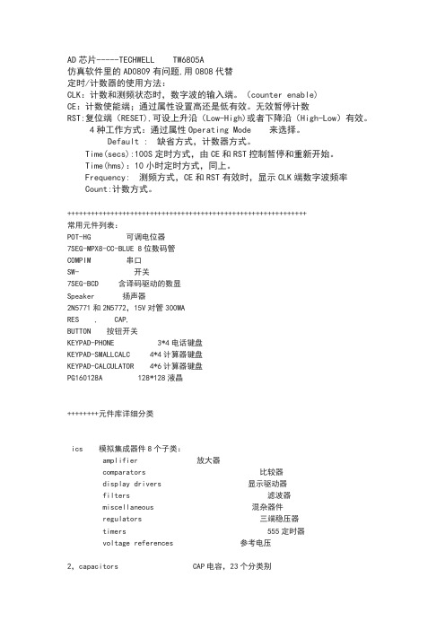
AD芯片-----TECHWELL TW6805A仿真软件里的AD0809有问题,用0808代替定时/计数器的使用方法:CLK:计数和测频状态时,数字波的输入端。
(counter enable)CE:计数使能端;通过属性设置高还是低有效。
无效暂停计数RST:复位端(RESET),可设上升沿(Low-High)或者下降沿(High-Low)有效。
4种工作方式:通过属性Operating Mode 来选择。
Default : 缺省方式,计数器方式。
Time(secs):100S定时方式,由CE和RST控制暂停和重新开始。
Time(hms):10小时定时方式,同上。
Frequency: 测频方式,CE和RST有效时,显示CLK端数字波频率Count:计数方式。
+++++++++++++++++++++++++++++++++++++++++++++++++++++++++++++常用元件列表:POT-HG 可调电位器7SEG-MPX8-CC-BLUE 8位数码管COMPIM 串口SW- 开关7SEG-BCD 含译码驱动的数显Speaker 扬声器2N5771和2N5772,15V对管300MARES , CAP,BUTTON 按钮开关KEYPAD-PHONE 3*4电话键盘KEYPAD-SMALLCALC 4*4计算器键盘KEYPAD-CALCULATOR 4*6计算器键盘PG160128A 128*128液晶++++++++元件库详细分类ics 模拟集成器件8个子类:amplifier 放大器comparators 比较器display drivers 显示驱动器filters 滤波器miscellaneous 混杂器件regulators 三端稳压器timers 555定时器voltage references 参考电压2,capacitors CAP电容,23个分类别animated 可显示充放电电荷电容audio grade axial 音响专用电容axial lead polypropene 径向轴引线聚丙烯电容axial lead polystyrene 径向轴引线聚苯乙烯电容ceramic disc 陶瓷圆片电容decoupling disc 解耦圆片电容high temp radial 高温径向电容high temp axial electrolytic高温径向电解电容metallised polyester film 金属聚酯膜电容metallised polypropene 金属聚丙烯电容metallised polypropene film 金属聚丙烯膜电容miniture electrolytic 微型电解电容multilayer metallised polyester film 多层金属聚酯膜电容mylar film 聚酯薄膜电容nickel barrier 镍栅电容non polarised 无极性电容polyester layer 聚酯层电容radial electrolytic 径向电解电容resin dipped 树脂蚀刻电容tantalum bead 钽珠电容variable 可变电容vx a xial electrolytic VX 轴电解电容3,CMOS 4000 series 4000系列数字电路adders 加法器buffers & drivers 缓冲和驱动器comparators 比较器counters 计数器decoders 译码器encoders 编码器flip-flops & latches 触发器和锁存器frequency dividers & tiner 分频和定时器gates & inverters 门电路和反相器memory 存储器混杂逻辑电路mutiplexers 数据选择器multivibrators 多谐振荡器phase-locked loops(PLL) 锁相环registers 寄存器signal switcher 信号开关4,connectors 接头;8个分类:audio 音频接头D-type D型接头DIL 双排插座header blocks 插头miscellaneous 各种接头PCB transfer PCB 传输接头SIL 单盘插座ribbon cable 蛇皮电缆terminal blocks 接线端子台5,data converters 数据转换器:4个分类:A/D converters 模数转换器D/A converters 数模转换器sample & hold 采样保持器temperature sensors 温度传感器6,debugging tools 调试工具数据:3个类别:breakpoint triggers 断点触发器logic probes 逻辑输出探针logic timuli 逻辑状态输入7,diodes 二极管;8个分类:bridge rectifiers 整流桥generic 普通二极管rectifiers 整流二极管schottky 肖特基二极管switching 开关二极管tunnel 隧道二极管varicap 稳压二极管8,inductors 电感:3个类别:generic 普通电感SMT inductors 表面安装技术电感transformers 变压器9,laplace primitives 拉普拉斯模型:7个类别:1st order 一阶模型2nd order 二阶模型controllers 控制器non-linear 非线性模型operators 算子poles/zeros 极点/零点symbols 符号10,memory ICs 存储器芯片:7个分类:dynamic RAM 动态数据存储器EEPROM 电可擦出程序存储器EPROM 可擦出程序存储器I2C memories I2C总线存储器memory cards 存储卡SPI Memories SPI总线存储器static RAM 静态数据存储器11,microprocessor ICs 微处理器:13个分类:12,modelling primitivvves 建模源:9个分类:13,operational amplifiers 运算放大器:7个分类:dual 双运放ideal 理想运放macromodel 大量使用的运放octal 8运放quad 4运放single 单运放triple 三运放14,optoelectronics 光电器件:11个分类:7-segment displays 7段显示alphanumeric LCDs 液晶数码显示bargraph displays 条形显示dot matrix displays 点阵显示graphical LCDs 液晶图形显示lamps 灯LCD controllers 液晶控制器LCD controllers 液晶面板显示LEDs 发光二极管optocouplers 光电耦合serial LCDs 串行液晶显示15,resistors 电阻:11个分类:metal film 金属膜电阻10 watt wirewound 10w绕线电阻2w metal film 2w 金属膜电阻3 watt wirewound 3w 绕线电阻7 watt wirewound 7w 绕线电阻generix 普通电阻high voltage 高压电阻NTC 负温度系数热敏电阻resistor packs 排阻variable 滑动变阻器varisitors可变电阻参考试验中采用的可变电阻是:POT-HG16,simulator primitives 仿真源:3个类别:flip-flops 触发器gates 门电路sources 电源17,switches and relays 开关和继电器:4个类别:key pads 键盘relays 普通继电器relays(specific) 专用继电器switches 开关18,switching devices 开关器件:4个分类:DIACs 两端交流开关generic 普通开关元件SCRs 可控硅TRIACs 三端双向可控硅19,真空管:20,传感器:2个分类:pressure 压力传感器temperature 温度传感器21,晶体管:8个分类:bipolar 双极型晶体管generic 普通晶体管(错误)IGBT 绝缘栅双极晶体管JFET 结型场效应管MOSFET 金属氧化物场效应管RF power LDMOS 射频功率LDMOS管RF power VDMOS 射频功率VDMOS管unijunction 单结晶体管Electromechanical 电机MOTOR AC 交流电机MOTOR SERVO 伺服电机双相步进电机motor-bistepper(Bipolar Stepper Motor),四相步进电机motor-stepper(unipolar stepper motor)驱动电路,用ULN2003可以,proteus中推荐的L298和L6201(电子元件-步进电机中有L298资料)+++++++++++++++++++++++++++++++++++++++++++++++++++++++++++++++++++++步进电机,可以用MTD2003,UN2916等专用芯片Proteus中图形液晶模块驱动芯片一览表LM3228 LM3229 LM3267 LM3283LM3287 LM4228 LM4265 LM4267LM4283 LM4287 PG12864F PG24064FPG128128A PG160128AAGM1232G EW12A03GLY HDM32GS12-B HDM32GS12Y-BHDG12864F-1 HDS12864F-3 HDG12864L-4 HDG12864L-6NOKIA7110 TG126410GFSB TG13650FEYAMPIRE128x64 LGM12641BS1RPROTEUS原理图元器件库详细说明单双向可控硅、包括电阻、电容、二极管、三极管和PCB的连接器符号、包括虚拟仪器和有源器件、拨动开关、键盘、可调电位器和开关、包括二极管和整流桥、稳压管、变容二极管、大功率二极管、高速二极管、可控硅、包括LCD、LED、LED阵列包括三极管包括场效应管包括模拟元器件AS 稳压二极管、全桥、74系列、及其他。
维希亚 Siliconix S12-1170-Rev. A 自动汽车N-通道 40V(D-S) 17

SQJ858AEP-T1-GE3SQJ858AEPVishay SiliconixAutomotive N-Channel 40 V (D-S) 175 °C MOSFETFEATURES•TrenchFET ® Power MOSFET •AEC-Q101 Qualified •100 % R g and UIS Tested•Material categorization:For definitions of compliance please see /doc?99912Notesa.Pulse test; pulse width ≤ 300 μs, duty cycle ≤ 2 %.b.When mounted on 1" square PCB (FR-4 material).c.Parametric verification ongoing.d.See solder profile (/doc?73257). The PowerPAK SO-8L is a leadless package. The end of the lead terminal is exposed copper (not plated) as a result of the singulation process in manufacturing. A solder fillet at the exposed copper tip cannot be guaranteed and is not required to ensure adequate bottom side solder interconnection.e.Rework conditions: manual soldering with a soldering iron is not recommended for leadless components.PRODUCT SUMMARYV DS (V)40R DS(on) (Ω) at V GS = 10 V 0.0063R DS(on) (Ω) at V GS = 4.5 V 0.0075I D (A)58ConfigurationSingleORDERING INFORMATIONPackagePowerPAK SO-8L Lead (Pb)-free and Halogen-freeSQJ858AEP-T1-GE3ABSOLUTE MAXIMUM RATINGS (T C = 25 °C, unless otherwise noted)PARAMETER S YMBOL LIMIT UNIT Drain-Source Voltage V DS40VGate-Source Voltage V GS ± 20Continuous Drain CurrentT C = 25 °C I D 58A T C = 125 °C33Continuous Source Current (Diode Conduction)I S 43Pulsed Drain Current aI DM 230Single Pulse Avalanche Current L = 0.1 mH I AS 35Single Pulse Avalanche Energy E AS 61mJ Maximum Power Dissipation aT C = 25 °C P D 48W T C = 125 °C 16Operating Junction and Storage Temperature Range T J , T stg- 55 to + 175°C Soldering Recommendations (Peak Temperature)d, e260THERMAL RESISTANCE RATINGSPARAMETER S YMBOL LIMIT UNIT Junction-to-Ambient PCB Mount bR thJA 85°C/WJunction-to-Case (Drain)R thJC3.1SQJ858AEPVishay SiliconixNotesa.Pulse test; pulse width ≤ 300 μs, duty cycle ≤ 2 %.b.Guaranteed by design, not subject to production testing.c.Independent of operating temperature.Stresses beyond those listed under “Absolute Maximum Ratings” may cause permanent damage to the device. These are stress ratings only, and functional operation of the device at these or any other conditions beyond those indicated in the operational sections of the specifications is not implied. Exposure to absolute maximum rating conditions for extended periods may affect device reliability.SPECIFICATIONS (T C = 25 °C, unless otherwise noted)PARAMETER S YMBOL TE S T CONDITION S MIN.TYP.MAX.UNITStaticDrain-Source Breakdown Voltage V DS V GS = 0, I D = 250 μA 40--V Gate-Source Threshold Voltage V GS(th)V DS = V GS , I D = 250 μA 1.5 2.0 2.5Gate-Source LeakageI GSS V DS = 0 V, V GS = ± 20 V--± 100nAZero Gate Voltage Drain Current I DSS V GS = 0 V V DS = 40 V --1μA V GS = 0 V V DS = 40 V, T J = 125 °C --50V GS = 0 V V DS = 40 V, T J = 175 °C--250On-State Drain Current aI D(on)V GS = 10 V V DS ≥ 5 V 30--A Drain-Source On-State Resistance aR DS(on)V GS = 10 VI D = 14 A -0.00500.0063ΩV GS = 4.5 V I D = 10 A -0.00600.0075V GS = 10 V I D = 14 A, T J = 125 °C --0.0120V GS = 10 VI D = 14 A, T J = 175 °C--0.0150Forward Transconductance b g fsV DS = 14 V, I D = 16 A-99-S Dynamic bInput Capacitance C issV GS = 0 V V DS = 20 V, f = 1 MHz -19512450pF Output CapacitanceC oss -295370Reverse Transfer Capacitance C rss -110140Total Gate Charge c Q gV GS = 10 V V DS = 20 V, I D = 20 A -3655nC Gate-Source Charge c Q gs -8-Gate-Drain Charge c Q gd -6-Gate Resistance R g f = 1 MHz1.52.97 4.5ΩTurn-On Delay Time c t d(on)V DD = 20 V, R L = 2 ΩI D ≅ 10 A, V GEN = 10 V, R g = 1 Ω-1015ns Rise Time ct r-914Turn-Off Delay Time c t d(off) -2640Fall Time c t f -812Source-Drain Diode Ratings and Characteristics bPulsed Current a I SM --230A Forward VoltageV SDI F = 15 A, V GS = 0-0.81.1VSQJ858AEP Vishay SiliconixTYPICAL CHARACTERISTICS (T A = 25 °C, unless otherwise noted)Output Characteristics TransconductanceCapacitanceTransfer CharacteristicsOn-Resistance vs. Drain CurrentGate ChargeSQJ858AEP Vishay SiliconixTYPICAL CHARACTERISTICS (T A = 25 °C, unless otherwise noted)Drain Source Breakdown vs. Junction TemperatureSQJ858AEP Vishay SiliconixTHERMAL RATINGS (T A = 25 °C, unless otherwise noted)Safe Operating AreaNormalized Thermal Transient Impedance, Junction-to-AmbientSQJ858AEP Vishay SiliconixTHERMAL RATINGS (T A = 25 °C, unless otherwise noted)Normalized Thermal Transient Impedance, Junction-to-CaseNote•The characteristics shown in the two graphs- Normalized Transient Thermal Impedance Junction-to-Ambient (25 °C)- Normalized Transient Thermal Impedance Junction-to-Case (25 °C)are given for general guidelines only to enable the user to get a “ball park” indication of part capabilities. The data are extracted from single pulse transient thermal impedance characteristics which are developed from empirical measurements. The latter is valid for the part mounted on printed circuit board - FR4, size 1" x 1" x 0.062", double sided with 2 oz. copper, 100 % on both sides. The part capabilities can widely vary depending on actual application parameters and operating conditions.Vishay Silicon ix main tain s worldwide man ufacturin g capability. Products may be man ufactured at on e of several qualified location s. Reliability data for Silicon Technology and Package Reliability represent a composite of all qualified locations. For related documents such as package/tape drawings, part marking, and reliability data, see /ppg?63470.Ordering Information Vishay SiliconixPowerPAK® SO-8LOrdering codes for the SQ rugged series power MOSFETs in the PowerPAK SO-8L package:DATASHEET PART NUMBER OLD ORDERING CODE a NEW ORDERING CODE SQJ200EP-SQJ200EP-T1_GE3SQJ202EP-SQJ202EP-T1_GE3SQJ401EP SQJ401EP-T1-GE3SQJ401EP-T1_GE3SQJ402EP SQJ402EP-T1-GE3SQJ402EP-T1_GE3SQJ403EEP SQJ403EEP-T1-GE3SQJ403EEP-T1_GE3SQJ403EP-SQJ403EP-T1_GE3SQJ410EP SQJ410EP-T1-GE3SQJ410EP-T1_GE3SQJ412EP SQJ412EP-T1-GE3SQJ412EP-T1_GE3SQJ422EP SQJ422EP-T1-GE3SQJ422EP-T1_GE3SQJ431EP SQJ431EP-T1-GE3SQJ431EP-T1_GE3SQJ443EP SQJ443EP-T1-GE3SQJ443EP-T1_GE3SQJ446EP-SQJ446EP-T1_GE3SQJ456EP SQJ456EP-T1-GE3SQJ456EP-T1_GE3SQJ459EP-SQJ459EP-T1_GE3SQJ460AEP-SQJ460AEP-T1_GE3SQJ461EP SQJ461EP-T1-GE3SQJ461EP-T1_GE3SQJ463EP SQJ463EP-T1-GE3SQJ463EP-T1_GE3SQJ465EP SQJ465EP-T1-GE3SQJ465EP-T1_GE3SQJ469EP SQJ469EP-T1-GE3SQJ469EP-T1_GE3SQJ486EP SQJ486EP-T1-GE3SQJ486EP-T1_GE3SQJ488EP SQJ488EP-T1-GE3SQJ488EP-T1_GE3SQJ500AEP SQJ500AEP-T1-GE3SQJ500AEP-T1_GE3SQJ840EP SQJ840EP-T1-GE3SQJ840EP-T1_GE3SQJ844AEP SQJ844AEP-T1-GE3SQJ844AEP-T1_GE3SQJ850EP SQJ850EP-T1-GE3SQJ850EP-T1_GE3SQJ858AEP SQJ858AEP-T1-GE3SQJ858AEP-T1_GE3SQJ886EP SQJ886EP-T1-GE3SQJ886EP-T1_GE3SQJ910AEP SQJ910AEP-T1-GE3SQJ910AEP-T1_GE3SQJ912AEP SQJ912AEP-T1-GE3SQJ912AEP-T1_GE3SQJ940EP SQJ940EP-T1-GE3SQJ940EP-T1_GE3SQJ942EP SQJ942EP-T1-GE3SQJ942EP-T1_GE3SQJ951EP SQJ951EP-T1-GE3SQJ951EP-T1_GE3SQJ952EP-SQJ952EP-T1_GE3SQJ956EP SQJ956EP-T1-GE3SQJ956EP-T1_GE3SQJ960EP SQJ960EP-T1-GE3SQJ960EP-T1_GE3SQJ963EP SQJ963EP-T1-GE3SQJ963EP-T1_GE3SQJ968EP SQJ968EP-T1-GE3SQJ968EP-T1_GE3SQJ980AEP SQJ980AEP-T1-GE3SQJ980AEP-T1_GE3SQJ992EP SQJ992EP-T1-GE3SQJ992EP-T1_GE3Notea.Old ordering code is obsolete and no longer valid for new ordersPackage Information Vishay SiliconixPowerPAK® SO-8L Case Outlinefor all PartsPackage InformationVishay SiliconixNote•Millimeters will goverLIMETERSINCHESMIN.NOM.MAX.MIN.NOM.MAX.A 1.00 1.07 1.140.0390.0420.045A10.00-0.1270.00-0.005b 0.330.410.480.0130.0160.019b10.440.510.580.0170.0200.023b2 4.804.905.000.1890.1930.197b30.0940.004b40.470.019c 0.200.250.300.0080.0100.012D 5.00 5.13 5.250.1970.2020.207D1 4.80 4.90 5.000.1890.1930.197D2 3.86 3.96 4.060.1520.1560.160D3 1.631.73 1.830.0640.0680.072e 1.27 BSC0.050 BSCE 6.05 6.15 6.250.2380.2420.246E1 4.27 4.37 4.470.1680.1720.176E2 2.75 2.85 2.950.1080.1120.116F --0.15--0.006L 0.620.720.820.0240.0280.032L10.921.07 1.220.0360.0420.048K 0.510.020W 0.230.009W10.410.016W2 2.820.111W3 2.960.117q0°-10°0°-10°ECN: C15-1203-Rev. A, 07-Sep-15DWG: 6044PAD PatternVishay SiliconixRevision: 07-Feb-121Document Number: 63818THIS DOCUMENT IS SUBJECT TO CHANGE WITHOUT NOTICE. THE PRODUCTS DESCRIBED HEREIN AND THIS DOCUMENTARE SUBJECT TO SPECIFIC DISCLAIMERS, SET FORTH AT /doc?91000RECOMMENDED MINIMUM PAD FOR PowerPAK ® SO-8L SINGLELegal Disclaimer Notice VishayDisclaimerALL PRODU CT, PRODU CT SPECIFICATIONS AND DATA ARE SU BJECT TO CHANGE WITHOU T NOTICE TO IMPROVE RELIABILITY, FUNCTION OR DESIGN OR OTHERWISE.Vishay Intertechnology, Inc., its affiliates, agents, and employees, and all persons acting on its or their behalf (collectively,“Vishay”), disclaim any and all liability for any errors, inaccuracies or incompleteness contained in any datasheet or in any other disclosure relating to any product.Vishay makes no warranty, representation or guarantee regarding the suitability of the products for any particular purpose or the continuing production of any product. To the maximum extent permitted by applicable law, Vishay disclaims (i) any and all liability arising out of the application or use of any product, (ii) any and all liability, including without limitation special, consequential or incidental damages, and (iii) any and all implied warranties, including warranties of fitness for particular purpose, non-infringement and merchantability.Statements regarding the suitability of products for certain types of applications are based on Vishay’s knowledge of typical requirements that are often placed on Vishay products in generic applications. Such statements are not binding statements about the suitability of products for a particular application. It is the customer’s responsibility to validate that a particular product with the properties described in the product specification is suitable for use in a particular application. Parameters provided in datasheets and/or specifications may vary in different applications and performance may vary over time. All operating parameters, including typical parameters, must be validated for each customer application by the customer’s technical experts. Product specifications do not expand or otherwise modify Vishay’s terms and conditions of purchase, including but not limited to the warranty expressed therein.Except as expressly indicated in writing, Vishay products are not designed for use in medical, life-saving, or life-sustaining applications or for any other application in which the failure of the Vishay product could result in personal injury or death. Customers using or selling Vishay products not expressly indicated for use in such applications do so at their own risk. Please contact authorized Vishay personnel to obtain written terms and conditions regarding products designed for such applications. No license, express or implied, by estoppel or otherwise, to any intellectual property rights is granted by this document or by any conduct of Vishay. Product names and markings noted herein may be trademarks of their respective owners.Material Category PolicyVishay Intertechnology, Inc. hereby certifies that all its products that are identified as RoHS-Compliant fulfill the definitions and restrictions defined under Directive 2011/65/EU of The European Parliament and of the Council of June 8, 2011 on the restriction of the use of certain hazardous substances in electrical and electronic equipment (EEE) - recast, unless otherwise specified as non-compliant.Please note that some Vishay documentation may still make reference to RoHS Directive 2002/95/EC. We confirm that all the products identified as being compliant to Directive 2002/95/EC conform to Directive 2011/65/EU.Vishay Intertechnology, Inc. hereby certifies that all its products that are identified as Halogen-Free follow Halogen-Free requirements as per JEDEC JS709A standards. Please note that some Vishay documentation may still make reference to the IEC 61249-2-21 definition. We confirm that all the products identified as being compliant to IEC 61249-2-21 conform to JEDEC JS709A standards.Revision: 02-Oct-121Document Number: 91000SQJ858AEP-T1-GE3。
乐信烤箱 Rational SCC_WE Modul

自动排水须满足下面 4 个条件:
1. 水箱累计工作时间必须大于 60 分钟.*
且
2. 水箱内的蒸汽热电偶的温度必须低于 65℃ (149华氏度)
29 31 32 33 34 35 36 37 38 39
40 41 42 43 44 45 46 47 48 49 50 51 52 54 55 56 57 60 64
66 67 68 70 71 72
V01e en, SCC_WE
基本原理 SCC_WE
排气管 单向阀
S2 水位电极
蒸汽水箱热电偶 B5 F3 干烧保护器
- 12 -
Survey Pictogram
进入技术服务菜单 日期和时间 开始时间 时间格式 24h 时间格式 am / pm 温度单位 ℃ - °F ½ 功率 设置铃声音调 演示模式 (显示为红色时) 显示屏亮度 分层的顺序 分层的数量 出厂设置 – 英语, ℃, 24 小时 等等 温差控制
确认 使用说明手册 安全提醒 CleanJet +Care 清洗保养控制
只要动过燃气部件,像: 燃气阀, 燃气鼓风机和 / 或 改变燃气类型 都必须用废气分析仪做全套的废气分析,CO 和 CO2 数值必须在合理范围 ! 该项工作必须由经过专业培训的技师完成! 每次都要检查燃气是否有泄漏!
请注意 任何有关 Rational 产品的技术资料不得转交给第三方
目录
初步介绍
基本原理 SCC_WE
自动排水结束后,蒸汽水箱的累计工作时间就会清零. SC- 自动排水不能取代水箱除垢 和 / 或 安装软水机
Mini-Circuits PWR-8P-RC 50

PWR-8P-RC50Ω -60 dBm to +20 dBm, 10 to 8000 MHzCASE STYLE: JL2441The Big Deal• Peak & average power of CW & pulse waveforms with pulse profiling• Measures power levels down to -60 dBm • Sample rate 500,000 samples per sec.• USB and Ethernet controlSm art Po wer SensorUSB / Ethernet Peak & AverageTrademarks: Windows is a registered trademark of Microsoft Corporation in the United States and other countries. Linux is a registered trademark of Linus Tor -valds. Mac is a registered trademark of Apple Corporation. Pentium is a registered trademark of Intel Corporation. Neither Mini-Circuits nor the Mini-Circuits PWR-series power sensors are affiliated with or endorsed by the owners of the above referenced trademarksMini-Circuits and the Mini-Circuits logo are registered trademarks of Scientific Components Corporation.Software PackageProduct OverviewMini-Circuits’ PWR-8P-RC is a compact sensor-head that turns any PC into a high performance power meter for peak and average measurements of CW and pulse modulated signals. The sensor has an 80 dB input dynamic range and wide bandwidth, allowing measurement of RF powers down to -60 dBm over 10 to 8000 MHz.The USB HID interface is “plug & play” compatible, meaning no driver installation is required, while the additional Ethernet interface allows remote power measurements over a network. Full software support is provided,including our user-friendly GUI application for Windows and a full API with programming instructions for Windows and Linux environments (both 32-bit and 64-bit systems). Download from /softwaredownload/pm.htmlTypical Applications• Pulse profiling & statistical signal analysis• Radar characterization (VHF / UHF / L / S / C bands)• Particle accelerator experimentation• Signal level calibration in production test systems• Power monitoring in remote installations / base-stationsModel No.DescriptionPWR-8P-RCUSB smart Power SensorIncluded Accessories PWR-SEN-8P-RC Power Sensor Head USB-CBL-AB-7+ 6.8 ft USB cableCBL-5FT-BMSMB+BNC(M) to SMB(F) Trigger cableRev. C M177005Generic photo used for illustration purposes onlyElectrical Specifications, -60 dBm to +20 dBm, 10 to 8000 MHz1 Maximum continuous safe operational power limit: +23 dBm.2Tested with CW signal3 Power uncertainty is specified for default semple period of 10ms.4 As sample period increases above 2.5 ms, resolution will decrease. If measuring a signal with duty cycle below 0.1% or over 99.9%, use the ‘Zoom on Pulse’ function in Pulse Profiling to get accurate peak and average measurements.5 Max sample rate is measured in thousands of samples per second (ksps). With sample periods greater than 2.5 msec the sample rate will be reduced to allow covering the full sample period.6 sensor’s internal rise time of 2.5 µs contributes an error to the measured rise time up to Mmax = √(R2 + 6.25) where R is the real rise time of the signal and M is the measured rise time indicatedby the sensor, so for example a signal with a 6µs rise may produce a measured rise time of up to √(signal rise time^2+sensor rise time^2)=√(6^2+2.5^2) =6.5µs (8.3% measurement error in rise time)7 When Ethernet control is enabled, it is recommended to use an external power supply (USB-AC/DC-5+ or equiv), a powered hub, or USB 3.0 port, as USB 2.0 ports are specified to suply 500mA load and thus may not be able to supply the required current.8 Internal trigger functions may not correctly identify a pulse lower than -48 dBm. If a trigger is needed for such signals it is recomended to use external trigger.Absolute Maximum RatingsOutline Drawing (JL2441)inch9 Maximum torque 8 in-lb (90 N-cm).RF Input (N Type-Male)Trigger In (SMB-Male)Trigger Out (SMB-Male)USB Port(USB type B female)Network (Ethernet/LAN)(RJ45 socket)Connections-8%-5%-2%1%4%7%10002000300040005000600070008000L i n e a r i t y (%)Frequency (MHz)LINEARITY @ 25O C1.001.061.121.181.241.3010002000300040005000600070008000V S W R (:1)FREQUENCY (MHz)VSWR-0.3-0.2-0.10.00.10.20.3010002000300040005000600070008000U N C E R T A I N T Y (d B )FREQUENCY (MHz)UNCERTAINTY OF POWER MEASUREMENTTypical Performance Curves-0.3-0.2-0.10.00.10.20.3010002000300040005000600070008000U N C E R T A I N T Y (d B )FREQUENCY (MHz)UNCERTAINTY OF POWER MEASUREMENTSoftware & Documentation Download:• Mini-Circuits’ full software and support package including user guide, Windows GUI, DLL files, programming manual and examples can be downloaded free of charge from/softwaredownload/pm.html .• Please contact ****************************** for supportGraphical User Interface (GUI) for Windows Key Features:• Set compensation frequency and monitor power measurement• Configure measurement (offsets, relative power readings, averaging, etc.)• Peak and average power measurement• Pulse profiling (see user guide and page 6 for details)• Internal and external trigger, Trigger and Video outputs• Graphical pulse display with ‘zoom on pulse’ feature (see user guide and page 6 for details)• Control multiple power sensors at once • Schedule data recordingApplication Programming Interface (API)Windows Support:• API DLL files exposing the full power sensor functionality • ActiveX COM DLL file for creation of 32-bit programs • .Net library DLL file for creation of 32 / 64-bit programs• HTTP Get/Post and Telnet protocols use SCPI commands to provide full control.• Supported by most common programming environments (refer to application note AN-49-001 for summary of tested environments)Linux Support:page 6 for detailsNote: Main screen powermeasurement will be accurate only for duty cycle 99.9% to 0.1%, for duty cycles outside this range need to use the ‘Zoom on Pulse’ function inPulse Profiling.Full pulse parameters are calculated and displayed in tabular form, including peak / average power, pulse width / period, duty cycle, rise / fall time, crest factor and overshoot.Note: If ‘zoom on pulse’ window is not showing the pulse signal calculated parameter may not be correctThe main pulse profile display shows the full sample period of the sensor in the time domain.Up to four markers can be set as required to measure power levels and calculate time / power deltas• Set the sample period between 10µs and 1s to capture the pulse profile•Select from 4 trigger options:1. Free – No trigger / free running measurements2. Internal – Detect and stabilise the measurements on the rising edge of the RF signal (not recomended for signals with pulse power below -48 dBm).3. Externala. Rising edge – Measurements are triggered on the rising edge of an external trigger signalb. Falling edge – Measurements are triggered on the falling edge of an external trigger signal•Enable external trigger / video output if required:a. External trigger provides a TTL output on the rising edge of a pulse for synchronization with external measurement equipmentb. Video output allows wider bandwidth pulses to be recorded by external measurement equipment Graphical User Interface - Pulse Profiling FeaturesFig 1: Main screen in Pulse Profiling configuration mode Fig 2: Graphical Pulse Profile - Full sample period“Zoom on pulse” feature will automatically zoom on the first identified pulse and allows any portion of the pulse profile to be focused on /expanded in a second graphical display, simply by ‘right clicking’ and dragging the mouse cursor over relevant section of the profile.Fig 3: Graphical Pulse Profile - “Zoom on Pulse”Fig 4: Calculated Pulse parametersFor signals with duty cycle greater than 99.9% or under 0.1% the automatic ‘zoom on pulse’ may not not work - in such cases you can adjust the zoom window by clicking on the arrow icons to increment/decrement the trigger delay and span, or the magnifying glass to type in precise values10µs - 1secConnection diagramsConnection diagram for USB controlConnection diagram for Ethernet control, using power adapterConnection diagram for Ethernet control, using PoE systemNote: Commercially available PoEsplitter not supplied by Mini-CircuitsUSB T ype A plug -power adaptorUSB-AC/DC-5Connect USB-AC/DC-5to mains powerUSB Type A plug -Included Accessories Part No.DescriptionPWR-SEN-8P-RCPower Sensor HeadUSB-CBL-AB-7+6.8 ft (2.1 m) USB Cable: USB type A(Male) to USB type B(Male)CBL-5FT-BMSMB+ 5 ft (1.5 m) Trigger cable: BNC(male) to SMB(Female)ModelDescriptionPWR-8P-RCUSB/Ethernet Smart Peak & Average Power SensorOrdering Information 10 Power plugs for other countries are also available, if you need a power plug for a country not listed in the table please contact testsolutions@ for support.11 Power adaptor, powered hub or USB 3.0 port may be used to provide power when in Ethernet control, not needed in USB control.Additional NotesA. Performance and quality attributes and conditions not expressly stated in this specification document are intended to be excluded and do not form a part of this specification document.B. Electrical specifications and performance data contained in this specification document are based on Mini-Circuit’s applicable established test performance criteria and measurement instructions.C. The parts covered by this specification document are subject to Mini-Circuits standard limited warranty and terms and conditions (collectively, “Standard Terms”); Purchasers of this part are entitled to the rights and benefits contained therein. For a full statement of the Standard Terms and the exclusive rights and remedies CalibrationDescriptionCALSEN-8P-RC Calibration ServiceClick HereOptional AccessoriesDescriptionUSB-AC/DC-5AC/DC 5V DC Power Adapter with US, EU, IL, UK, AUS, and China power plugs 10,11USB-CBL-AB-3+ 2.7 ft (0.8 m) USB Cable: USB type A(Male) to USB type B(Male)USB-CBL-AB-7+ (spare) 6.8 ft (2.1 m) USB Cable: USB type A(Male) to USB type B(Male)CBL-RJ45-MM-5+5 ft (1.5 m) Ethernet cable: RJ45(Male) to RJ45(Male) Cat 5E cable CBL-5FT-BMSMB+(spare) 5 ft (1.5 m) Trigger cable: BNC(male) to SMB(Female) NF-SM50+N-Type Female to SMA Male Adapter.NF-SF50+N-Type Female to SMA Female Adapter NF-BM50+N-Type Female to BNC Male Adapter.10 Power Sensor to be used with the supplied control cable only.。
SMC Wiring Assembly Socket 型号 WIREFOX-D 11, WIREFO

8 mm Electric
suitable ferrules to the end of each wire.
Shield ∗1
wire
Pin terminal ferrule (recommended)
∗1: CC-Link, DeviceNet ®
Gasket
12 mm
29 mm
URL https://
Body
Make sure the connector has no loosing.
Note
Please do not use it for purposes other than the original purpose. This connector may only be operated when under no load. Working with wet hands causes electric shock. Please never perform a repair. When pulling the lock lever, it may get damaged when tools such as a flat blade screwdriver are used due to the application of excessive force.
Product Construction
Please check contents.
∗: The photograph shows socket type.
Cap
Gasket Shield foil Body
Body
Assembly
First slide the Cap, Gasket and Body over the cable.
1271A
3
CS
Current Sense
4
Gnd
IC Ground
5
Drv
Driver Output
6
VCC
Supply Voltage
8
HV
High Voltage
Description
A resistor to ground provides the adjustable standby skip level. Additionally, if this pin is pulled higher than 8.0 V (typical), the controller latches off the drive.
NCP1271
Skip/ latch 1
I skip
Rskip
10V
4.8 V
8V
+
13 us filter
latch-off, reset
S
when Vcc < 4V
RQ
Vskip = Rskip * Iskip or Vskip = 1.2 V when pin 1 is opened
V skip skip
Rramp
+
43ĂmVńms 8.1ĂmAńms
+
5.3ĂkW
(eq. 4)
It is recommended that the value of Rramp be limited to less then 10 kW. Values larger than this will begin to limit the effective duty cycle of the controller and may result in
柯蒂斯电控资料
科蒂斯CURTIS系列电动汽车电机控制系统系列产品技术资料由于是进口产品!中文资料较少!这是我花费了不少时间搜集整理出来的!型号:1204/1205:串励电机速度控制器类型:电压:24-48V;电流:175-400A适用范围:科蒂斯1204/1205/1209型串励电机速度控制器是多种工业电动车辆的理想选择。
广泛应用于电动搬运车、电动装载车、物料搬运车、高尔夫球车以及其他小型串励机设备应用场合。
型号:1207A:串励电机速度控制器(CURTIS/PMC1270A)类型:额定电流:250A/300A;额定电压:24V。
可编程适用范围:可编程科蒂斯1207A型串励电机速度控制器是小型电动车辆的理想选择。
广泛应用于电动托盘车、堆垛车、电动搬运车、清扫车以及其他小型串励和复励电机设备应用场合。
型号:科蒂斯1209B:串励电机速度控制器类型:电压:36-48V/48-72V电流:400-450A适用范围:是多种工业电动车辆的理想选择。
广泛应用于电动搬运车、电动装载车、物料搬运车、高尔夫球车以及其他小型串励电机设备应用场合。
类型:科蒂斯1210:永磁电机速度控制器:类型:符合欧洲及美国标准,可编程。
电压:24V;电流:45A/70A适用范围:科蒂斯1210型永磁电机速度控制器适用于3-4轮的电动休闲车及代步车及清扫车等小型工业车辆。
型号:科蒂斯1214/1215/1219类型:可编程额定电压:48V额定电流:250A/300A/400A/500A/600A;适用范围:是电动车辆的理想选择。
广泛应用于电动托盘车、堆垛车、电动搬运车、清扫车以及其他小型串励和复励电机设备应用场合。
串励电机速度控制器。
型号:科蒂斯1221B串励电机速度控制器类型:24-36 V, 600 A;36-48 V, 550 A;48-72 V, 500 A适用范围:是多种工业电动车辆的理想选择。
广泛应用于电动搬运车、电动装载车、物料搬运车、高尔夫球车以及其他小型串励电机设备应用场合。
NCP1271D65R2G 笔记本适配器AC-DC电源管理芯片
NCP1271
Soft-Skipt Mode Standby PWM Controller with Adjustable Skip Level and External Latch
The NCP1271 represents a new, pin to pin compatible, generation of the successful 7−pin current mode NCP12XX product series. The controller allows for excellent stand by power consumption by use of its adjustable Soft−Skip mode and integrated high voltage startup FET. This proprietary Soft−Skip also dramatically reduces the risk of acoustic noise. This allows the use of inexpensive transformers and capacitors in the clamping network. Internal frequency jittering, ramp compensation, timer−based fault detection and a latch input make this controller an excellent candidate for converters where ruggedness and component cost are the key constraints.
Vishay Semiconductors VOM1271 光电 MosFET 驱动器说明书
Photovoltaic MOSFET Driver with Integrated Fast Turn-Off,Solid-State RelayDESCRIPTIONThe VOM1271 is a stand-alone optically isolated MOSFET driver. Unlike conventional MOSFET drivers, which require an external power supply to provide V CC and or V DD rails to the driver itself, the VOM1271 obtains all the required current to drive its internal circuitry from the LED current on the low voltage primary side of the isolation barrier. This saves the designer the space and cost associated with providing one or more external power supplies. The VOM1271 also integrates a turn-off circuit internal to the component itself, thus doing away with the need for additional components in order to increase the overall switching speed by decreasing the turn-off time. These features, combined with a small SOP4 package, provide designers with a small footprint, highly integrated isolated gate driver solution for a large variety of MOSFET drive applications.FEATURES•Open circuit voltage at I F = 10 mA, 8.4 V typical•Short circuit current at I F = 10 mA, 15 μA typical •Isolation test voltage 4500 V RMS •Logic compatible input •High reliability•Integrated rapid turn-off circuitry•Material categorization:For definitions of compliance please see /doc?99912APPLICATIONS•High-side driver •Solid-state relays •Floating power supply •Power control •Data acquisition •ATE•Isolated solenoid drivers •Isolated high current relay drivers •Isolated high voltage relay driversAGENCY APPROVALSThe safety application model number covering all products in this datasheet is VOM1271. This model number should be used when consulting safety agency documents.•UL1577•cUL, equivalent to CSA bulletin 5A •FIMKO EN 60950-1SAFETY AGENCY COMPLIANCEPlease see document: /doc?83743Note•For additional information on the available options refer to option information. The product is available only on tape and reel.i179066_6Notes•Stresses in excess of the absolute maximum ratings can cause permanent damage to the device. Functional operation of the device is not implied at these or any other conditions in excess of those given in the operational sections of this document. Exposure to absolute maximum ratings for extended periods of the time can adversely affect reliability.(1)Refer to reflow profile for soldering conditions for surface mounted devices (SOP).Note•Minimum and maximum values are testing requirements. Typical values are characteristics of the device and are the result of engineering evaluations. Typical values are for information only and are not part of the testing requirements.Fig. 1 - t on , t off Test Circuit and WaveformsABSOLUTE MAXIMUM RATINGS (T amb = 25 °C, unless otherwise specified)PARAMETER TEST CONDITIONSYMBOLVALUE UNIT SSRLED input ratings continous forward current I F50mA LED input ratings reverse voltage I R ≤ 10 μAV R 5V Ambient operating temperature range T amb - 40 to + 100°C Storage temperature range T stg- 40 to + 125°C Pin soldering temperature (1)t ≤ 10 s max.T sld 260°C Isolation test voltagebetween emitter and detectort = 1 sV ISO4500V RMSELECTRICAL CHARACTERISTICS (T amb = 25 °C, unless otherwise specified)PARAMETER TEST CONDITIONSYMBOLMIN.TYP.MAX.UNIT LED forward voltageI F = 10 mA V F 1.21.4 1.6V Open circuit voltageI F = 5 mAV OC 8.1V I F = 10 mA V OC 7.88.4V I F = 20 mA V OC 8.7V I F = 30 mA V OC 8.9V Short circuit currentI F = 5 mAI SC 7.0μA I F = 10 mA ISC 6.015.0μA I F = 20 mA I SC 30.0μA I F = 30 mAI SC47.0μASWITCHING CHARACTERISTICS (T amb = 25 °C, unless otherwise specified)PARAMETER TEST CONDITION SYMBOLMIN.TYP.MAX.UNIT Turn-on time C L = 200 pF, I F = 20 mA,P W = 2 ms, duty cycle = 50 %t on 53μs Turn-off timet off24μsTYPICAL CHARACTERISTICS (T amb = 25 °C, unless otherwise specified)Fig. 2 - Output Open Circuit Voltage vs. LED CurrentFig. 3 - Output Short-Circuit Current vs. Ambient TemperatureFig. 4 - Output Open Circuit Voltage vs. Ambient TemperatureFig. 5 - t on , t off vs. LED CurrentSAFETY AND INSULATION RATINGSPARAMETERTEST CONDITION SYMBOLMIN.TYP.MAX.UNITClimatic classification (according to IEC 68 part 1)IEC 68 part 140/100/21Comparative tracking index Insulation group IIIaCTI 175399Transient overvoltage V IOTM 6000V Recurring peak voltage V IORM 630V Package safety power P SO 350mW Package safety current I SI 150mA Package safety temperature T SI175°C Creepage distance 5mm Clearance distance5mmFig. 6 - LED Reverse Current vs. Reverse VoltageFig. 7 - LED Forward Voltage vs. LED Forward CurrentFig. 8 - Short Circuit Output Current vs.Open Circuit Output VoltageAPPLICATION DESCRIPTIONFigure 8 illustrates a standard isolated MOSFET driver such as Vishay’s VO1263. Though these parts are generally capable of supplying higher output current, they lack integrated fast turn-off circuitry. Thus, if high turn-off speed is required. external circuitry needs to be provided, as illustrated in figure one.Figure 9 illustrates the ability to do away with external turn-off circuitry with the VOM1271, by taking advantage of the VOM1271’s integrated turn-off circuitry.Fig. 9 - Typical MOSFET Driver Application without Integrated Fast Turn-OffFig. 10 - Typical MOSFET Driver Applications with Integrated Fast Turn-OffPACKAGE DIMENSIONS in millimetersPACKAGE MARKING (example)TAPE AND REEL PACKAGING Dimensions in millimetersFig. 11 - Tape and Reel Shipping Medium (EIA-481, revision A, and IEC 60286), 2000 units per reel Fig. 12 - Tape DimensionsLegal Disclaimer Notice VishayDisclaimerALL PRODUCT, PRODUCT SPECIFICAT IONS AND DAT A ARE SUBJECT T O CHANGE WIT HOUT NOT ICE T O IMPROVE RELIABILITY, FUNCTION OR DESIGN OR OTHERWISE.Vishay Intertechnology, Inc., its affiliates, agents, and employees, and all persons acting on its or their behalf (collectively, “Vishay”), disclaim any and all liability for any errors, inaccuracies or incompleteness contained in any datasheet or in any other disclosure relating to any product.Vishay makes no warranty, representation or guarantee regarding the suitability of the products for any particular purpose or the continuing production of any product. To the maximum extent permitted by applicable law, Vishay disclaims (i) any and all liability arising out of the application or use of any product, (ii) any and all liability, including without limitation special, consequential or incidental damages, and (iii) any and all implied warranties, including warranties of fitness for particular purpose, non-infringement and merchantability.Statements regarding the suitability of products for certain types of applications are based on Vishay’s knowledge of typical requirements that are often placed on Vishay products in generic applications. Such statements are not binding statements about the suitability of products for a particular application. It is the customer’s responsibility to validate that a particular product with the properties described in the product specification is suitable for use in a particular application. Parameters provided in datasheets and / or specifications may vary in different applications and performance may vary over time. All operating parameters, including typical parameters, must be validated for each customer application by the customer’s technical experts. Product specifications do not expand or otherwise modify Vishay’s terms and conditions of purchase, including but not limited to the warranty expressed therein.Except as expressly indicated in writing, Vishay products are not designed for use in medical, life-saving, or life-sustaining applications or for any other application in which the failure of the Vishay product could result in personal injury or death. Customers using or selling Vishay products not expressly indicated for use in such applications do so at their own risk. Please contact authorized Vishay personnel to obtain written terms and conditions regarding products designed for such applications.No license, express or implied, by estoppel or otherwise, to any intellectual property rights is granted by this document or by any conduct of Vishay. Product names and markings noted herein may be trademarks of their respective owners.© 2017 VISHAY INTERTECHNOLOGY, INC. ALL RIGHTS RESERVEDMouser ElectronicsAuthorized DistributorClick to View Pricing, Inventory, Delivery & Lifecycle Information:V ishay:VOM1271T。
- 1、下载文档前请自行甄别文档内容的完整性,平台不提供额外的编辑、内容补充、找答案等附加服务。
- 2、"仅部分预览"的文档,不可在线预览部分如存在完整性等问题,可反馈申请退款(可完整预览的文档不适用该条件!)。
- 3、如文档侵犯您的权益,请联系客服反馈,我们会尽快为您处理(人工客服工作时间:9:00-18:30)。
SC1271KInnoSwitch FamilyJune 2015Off-Line CV/CC Flyback Switcher IC with Integrated MOSFET, Synchronous Rectification and FeedbackThis Product is Covered by Patents and/or Pending Patent Applications.Product HighlightsHighly Integrated, Compact Footprint• Incorporates flyback controller, 725 V MOSFET, secondary-sidesensing and synchronous rectification driver• Integrated FluxLink ™, HIPOT-isolated, feedback link • E xceptional CV/CC accuracy, independent of transformer design or external components • I nstantaneous transient response ±5% CV with 0%-100%-0% load stepEcoSmart ™– Energy Efficient• <10 mW no-load at 230 VAC when supplied by transformer biaswinding • E asily meets all global energy efficiency regulations • L ow heat dissipationAdvanced Protection / Safety Features• Primary sensed output OVP •S econdary sensed output overshoot clamp •S econdary sensed output OCP to zero output voltage •H ysteretic thermal shutdown Full Safety and Regulatory Compliance• 100% production HIPOT compliance testing at 6 kV DC/1 sec • Reinforced insulation• Isolation voltage >3,500 VAC•U L1577 and TUV (EN60950) safety approved •EN61000-4-8 (100 A/m) and EN61000-4-9 (1000 A/m) compliantGreen Package• H alogen free and RoHS compliantApplications• C hargers and adapters for smart mobile devices • H igh efficiency, low voltage, high current power suppliesDescriptionThe InnoSwitch ™ family of ICs dramatically simplifies the development and manufacturing of low-voltage, high current power supplies,particularly those in compact enclosures or with high efficiency require-ments. The InnoSwitch architecture is revolutionary in that the devices incorporate both primary and secondary controllers, with sense elements and a safety-rated feedback mechanism into a single IC.Close component proximity and innovative use of the integrated communication link permit accurate control of a secondary-side synchronous rectification MOSFET and optimization of primary-side switching to maintain high efficiency across the entire load range. Additionally, the minimal DC bias requirements of the link enables the system to achieve less than 10 mW no-load in challenging applications such as smart-mobile device chargers.Output Power TableProduct 385-265 VACAdapter 1Peak or Open Frame 2SC1271K20 W25 WTable 1. Output Power Table.Notes:1. Minimum continuous power in a typical non-ventilated enclosed typical size adapter measured at 40 °C ambient. Max output power is dependent on the design. With condition that package temperature must be < = 125 °C.2. Minimum peak power capability.3. Package: eSOP-R16B.Figure 2. High Creepage, Safety-Compliant eSOP Package.PI-7519-020615OV O 1295C o n s t a n t V o l t a g e (C V )Constant Current (CC)PI-7146-121213(a) Typical Application Schematic(b) Output CharacteristicFigure 1. Typical Application/Performance.Figure 3. Primary-Side Controller Block Diagram.Figure 4. Secondary-Side Controller Block Diagram. Figure 5. Pin Configuration.Pin Functional DescriptionDRAIN (D) Pin (Pin 1)This pin is the power MOSFET drain connection.SOURCE (S) Pin (Pin 3-6)This pin is the power MOSFET source connection. It is also theground reference for the BYPASS and FEEDBACK pins.PRIMARY BYPASS (BPP) Pin (Pin 7)It is the connection point for an external bypass capacitor for the primary IC supply.FORWARD (FWD) Pin (Pin 10)The connection point to the switching node of the transformer output winding for sensing and other functions.OUTPUT VOLTAGE (VOUT) Pin (Pin 11)This pin is connected directly to the output voltage of the power supply to provide bias to the secondary IC.SYNCHRONOUS RECTIFIER DRIVE (SR) Pin (Pin 12) Connection to external SR FET gate terminal.SECONDARY BYPASS (BPS) Pin (Pin 13)It is the connection point for an external bypass capacitor for the secondary IC supply.FEEDBACK (FB) Pin (Pin 14)This pin connects to an external resistor divider to set the power supply CV voltage regulation threshold.SECONDARY GROUND (GND) (Pin 15)Ground connection for the secondary IC.ISENSE (IS) Pin (Pin 16)Connection to the power supply output terminals. Internal current sense is connected between this pin and the SECONDARY GROUND pin.Absolute Maximum Ratings 1,2DRAIN Pin Voltage ....................................................-0.3 V to 725 V DRAIN Pin Peak Current 3 .........................................1680 (3150) mA PRIMARY BYPASS/SECONDARY BYPASS Pin Voltage ........-0.3 V to 9 V PRIMARY BYPASS/SECONDARY BYPASS Pin Current ...............100 mA FORWARD Pin Voltage ..............................................-1.5 V to 150 V FEEDBACK Pin Voltage ....................................................-0.3 to 9 V 6SR/P Pin Voltage ..............................................................-0.3 to 9 V OUTPUT VOLTAGE Pin Voltage ........................................-0.3 to 15 V Storage Temperature ...................................................-65 to 125 °C Operating Junction Temperature 4,6 ...............................-40 to 125 °C Ambient Temperature ...................................................-40 to 85 °C Lead Temperature 5 ................................................................260 °CNotes:1. All voltages referenced to Source and Secondary Ground, T A = 25 °C.2. Maximum ratings specified may be applied one at a time without causing permanent damage to the product. Exposure to Absolute Maximum Ratings conditions for extended periods of time may affect product reliability.3. Higher peak Drain current is allowed while the Drain voltage is simultaneously less than 400 V.4. Normally limited by internal circuitry.5. 1/16” from case for 5 seconds.6. -1.8 V for a duration of ≤500 nsec.7. Maximum silicon operating junction temperature is 150 °C, however safety agency maximum operating junction is 125 °C.8. The maximum current out of the FORWARD pin when the FORWARD pin is below Ground is -40 mA.9. Maximum current into VOUT pin at 15 V should not exceed 10 mA.Thermal ResistanceThermal Resistance: eSOP-R16B Package: (q JA ).......................... ................65 °C/W 2, 69 °C/W 1(q JC ) .......................................................12 °C/W 3Notes:1. Solder to 0.36 sq. in (232 mm 2), 2 oz. (610 g/m 2) copper clad.2. Solder to 1 sq. in (645 mm 2), 2 oz. (610 g/m 2) copper clad.3. The case temperature is measured at the plastic surface at the top of the package.NOTES:A. This parameter is derived from characterization.B. I S1 is an estimate of device current consumption at no-load, since the operating frequency is so low under these conditions. Total deviceconsumption at no-load is sum of I S1 and I DSS2 (this does not include secondary losses)C. Since the output MOSFET is switching, it is difficult to isolate the switching current from the supply current at the Drain. An alternative is to measure the PRIMARY BYPASS pin current at 6.2 V.D. The PRIMARY BYPASS pin is not intended for sourcing supply current to external circuitry.E. To ensure correct current limit it is recommended that nominal 0.1 m F/1 m F/10 m F capacitors are used. In addition, the BPP capacitor valuetolerance should be equal or better than indicated below across the ambient temperature range of the target application. The minimum and maximum capacitor values are guaranteed by characterization.F. This parameter is derived from the change in current limit measured at 1X and 4X of the di/dt shown in the I LIMIT specification.G. Auto-restart on-time has same temperature characteristics as the oscillator (inversely proportional to frequency).H. I DSS1 is the worst-case OFF-state leakage specification at 80% of BV DSS and the maximum operating junction temperature. I DSS2 is a typicalspecification under worst-case application conditions (rectified 230 VAC) for no-load consumption calculations.I. Breakdown voltage may be checked against minimum BV DSS specification by ramping Drain voltage up to but not exceeding minimum BV DSS .J. For reference only. This is the total range of current limit threshold which corrects for variations in the current sense bond wire. Both of which are trimmed to set the normalized output constant current.K. Measured at the VOUT pin of the device. At the end of the cable under-load, the apparent auto-restart threshold will be lower.Nominal PRIMARY BYPASS Pin Capacitor Value Tolerance Relative to Nominal Capacitor Value Minimum Maximum0.1 m F -60%+100%1 m F -50%+100%10 m F -50%N/APart Ordering TableProduct Cable CompensationSC1271K6%For the latest updates, visit our website: Power Integrations reserves the right to make changes to its products at any time to improve reliability or manufacturability. Power Integrations does not assume any liability arising from the use of any device or circuit described herein. POWER INTEGRATIONS MAKES NO WARRANTYHEREIN AND SPECIFICALLY DISCLAIMS ALL WARRANTIES INCLUDING, WITHOUT LIMITATION, THE IMPLIED WARRANTIES OF MERCHANTABILITY, FITNESS FOR A PARTICULAR PURPOSE, AND NON-INFRINGEMENT OF THIRD PARTY RIGHTS.Patent InformationThe products and applications illustrated herein (including transformer construction and circuits external to the products) may be covered by one or more U.S. and foreign patents, or potentially by pending U.S. and foreign patent applications assigned to Power Integrations. A complete list of Power Integrations patents may be found at . Power Integrations grants its customers a license under certain patent rights as set forth at /ip.htm.Life Support PolicyPOWER INTEGRATIONS PRODUCTS ARE NOT AUTHORIZED FOR USE AS CRITICAL COMPONENTS IN LIFE SUPPORT DEVICES OR SYSTEMS WITHOUT THE EXPRESS WRITTEN APPROVAL OF THE PRESIDENT OF POWER INTEGRATIONS. As used herein:1. A Life support device or system is one which, (i) is intended for surgical implant into the body, or (ii) supports or sustains life, and (iii) whosefailure to perform, when properly used in accordance with instructions for use, can be reasonably expected to result in significant injury or death to the user.2. A critical component is any component of a life support device or system whose failure to perform can be reasonably expected to cause thefailure of the life support device or system, or to affect its safety or effectiveness.The PI logo, TOPSwitch, TinySwitch, LinkSwitch, LYTSwitch, InnoSwitch, DPA-Switch, PeakSwitch, CAPZero, SENZero, LinkZero, HiperPFS, HiperTFS, HiperLCS, Qspeed, EcoSmart, Clampless, E-Shield, Filterfuse, FluxLink, StakFET, PI Expert and PI FACTS are trademarks of Power Integrations, Inc. Other trademarks are property of their respective companies. ©2015, Power Integrations, Inc.World Headquarters 5245 Hellyer AvenueSan Jose, CA 95138, USA.Main: +1-408-414-9200Customer Service:Phone: +1-408-414-9665Fax: +1-408-414-9765e-mail: usasales@ China (Shanghai)Rm 2410, Charity Plaza, No. 88North Caoxi RoadShanghai, PRC 200030Phone: +86-21-6354-6323Fax: +86-21-6354-6325e-mail: chinasales@China (Shenzhen)17/F, Hivac Building, No. 2, Keji Nan 8th Road, Nanshan District, Shenzhen, China, 518057Phone: +86-755-8672-8689Fax: +86-755-8672-8690e-mail: chinasales@GermanyLindwurmstrasse 11480337 Munich GermanyPhone: +49-895-527-39110Fax: +49-895-527-39200e-mail: eurosales@ India#1, 14th Main Road VasanthanagarBangalore-560052 India Phone: +91-80-4113-8020Fax: +91-80-4113-8023e-mail: indiasales@ItalyVia Milanese 20, 3rd. Fl.20099 Sesto San Giovanni (MI) Italy Phone: +39-024-550-8701Fax: +39-028-928-6009e-mail: eurosales@ JapanKosei Dai-3 Bldg.2-12-11, Shin-Yokohama, Kohoku-kuYokohama-shi Kanagwan 222-0033 JapanPhone: +81-45-471-1021Fax: +81-45-471-3717e-mail: japansales@Korea RM 602, 6FL Korea City Air Terminal B/D, 159-6Samsung-Dong, Kangnam-Gu,Seoul, 135-728, Korea Phone: +82-2-2016-6610Fax: +82-2-2016-6630e-mail: koreasales@ Singapore51 Newton Road#19-01/05 Goldhill Plaza Singapore, 308900Phone: +65-6358-2160Fax: +65-6358-2015e-mail: singaporesales@Taiwan5F, No. 318, Nei Hu Rd., Sec. 1Nei Hu Dist.Taipei 11493, Taiwan R.O.C.Phone: +886-2-2659-4570Fax: +886-2-2659-4550e-mail: taiwansales@UKFirst Floor, Unit 15, Meadway Court,Rutherford Close, Stevenage, Herts. SG1 2EF United Kingdom Phone: +44 (0) 1252-730-141Fax: +44 (0) 1252-727-689e-mail: eurosales@ Power Integrations Worldwide Sales Support LocationsRevisionNotes Date A Initial Release.04/15BChanged Bypass Capacitor selection and limit on non-critical parameters.06/15。