全差分_伪差分_单端输入ADC理解
ADC的多种输入类型介绍
ADC的多种输入类型介绍ADC(Analog-to-Digital Converter)是模拟信号转换为数字信号的设备或电路。
它是现代电子系统中不可或缺的组成部分,用于将来自各种传感器、电源、音频设备等的模拟信号转化为数字信号,以便于数字处理、存储和传输。
根据不同的应用需求,ADC可以接受多种输入类型。
以下是几种常见的ADC输入类型及其特点。
1. 单端输入(Single-Ended Input):单端输入是最常见的ADC输入类型,它接受来自一个信号源的单个信号输入。
例如,一个温度传感器可以通过单端输入将模拟温度信号转化为数字形式。
单端输入的优势是简单易用,但由于信号只有一种极性,有时可能会受到噪声的影响。
2. 差分输入(Differential Input):差分输入允许两个信号源之间的差异信号被转换为数字信号。
差分输入可以提供更好的抗干扰能力和动态范围。
它可以使用两个相位相反但幅度相等的信号来消除共模噪声,提高信号的准确性和可靠性。
差分输入常用于音频设备和精密测量仪器等需要高质量信号转换的应用。
3. 伪差分输入(Pseudo-Differential Input):伪差分输入是一种介于单端输入和差分输入之间的输入方式。
它接受单个信号源的信号输入,但采用了与差分输入相似的电路拓扑结构,以提供一些差分输入的特性。
伪差分输入可以减少来自共模噪声的影响,并在成本和复杂度方面相对较低,因此在一些需要一定抗干扰性能的应用中得到应用。
4. 压缩输入(Ratiometric Input):压缩输入是一种将传感器输出信号与电源电压进行比较的输入方式。
这种输入方式主要用于传感器输出的电压与电源电压有关联的情况,比如热敏电阻器(thermistor)或光敏二极管(photodiode)。
在这种情况下,ADC会测量传感器输出相对于电源电压的比例,从而消除电源电压的波动对转换结果的影响。
5. 高电压输入(High Voltage Input):高电压输入是指ADC可以接受高于其供电电压的信号输入。
ADC的多种输入类型介绍
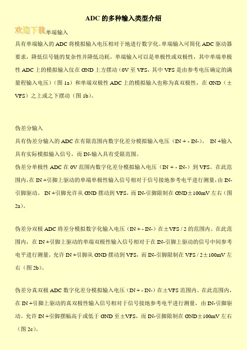
ADC的多种输入类型介绍单端输入具有单端输入的ADC将模拟输入电压相对于地进行数字化。
单端输入可简化ADC驱动器要求,降低信号链的复杂性并降低功耗。
单端输入可以是单极性或双极性,其中单端单极性ADC上的模拟输入仅在GND上方摆动(0V至VFS,其中VFS是由参考电压确定的满量程输入电压)(图1a)和单端双极性ADC上的模拟输入也称为真双极性,在GND(±VFS)之上或之下摆动(图1b)。
伪差分输入具有伪差分输入的ADC在有限范围内数字化差分模拟输入电压(IN + - IN-)。
IN +输入具有实际模拟输入信号,而IN-输入具有受限范围。
伪差分单极性ADC在0V范围内数字化差分模拟输入电压(IN + - IN-)到VFS。
在此范围内,在IN +引脚上驱动的单端单极性输入信号相对于信号接地参考电平进行测量,由IN-引脚驱动。
IN +引脚允许从GND摆动到VFS,而IN-引脚限制在GND±100mV左右(图2a)。
伪差分双极ADC将差分模拟数字化输入电压(IN + - IN-)在±VFS / 2的范围内。
在此范围内,在IN +引脚上驱动的单端双极性输入信号相对于在IN-引脚上驱动的信号中间参考电平进行测量。
允许IN +引脚从GND摆动到VFS,而IN-引脚限制在VFS / 2±100mV左右(图2b)。
伪差分真双极ADC数字化差分模拟输入电压(IN + - IN-)在±VFS范围内。
在此范围内,在IN +引脚上驱动的真双极性输入信号相对于信号接地参考电平进行测量,由IN-引脚驱动。
允许IN +引脚摆幅高于或低于GND至±VFS,而IN-引脚限制在GND±100mV左右(图2c)。
AN1108-了解单端、伪差分和全差分ADC

了解单端、伪差分和全差分ADC当今许多仪器仪表和过程控制应用程序使用模数转换器(ADC)转换传感器的模拟输出,以进行处理和/或存储。
对于电压输入 ADC,存在三种不同的输入结构类型:单端、伪差分和全差分。
本教程解释了输入类型之间的差异、优势和权衡。
今天的许多电子仪器依靠微控制器或数字信号处理器(DSP来处理真实世界的模拟信号。
传感器将温度或压力等自然参数转换为电压或电流。
模数转换器(ADC或A/D转换器)将信号转换成数字形式。
对于电压输入 ADC,存在三种不同的输入结构类型:单端、伪差分和全差分。
最简单的解决方案是选择与传感器输出相匹配的ADC输入结构。
然而,每种结构都有需要考虑的权衡。
此外,如果在传感器和 ADC之间使用信号调节电路,则该电路会影响 ADC输入结构的选择。
有些ADC是可配置的,允许在单端或伪差分输入结构(MAX186、MAX147)之间进行选择,而其他ADC则允许在单端或全差分(MAX1298、MAX1286)之间进行选择。
全差分输入为了最大限度地抑制噪声,使用全差分输入。
图1显示了一个全差分 ADC T/H输入结构的示例。
在充电模式下 Csample+对[AIN+ Vdd/2]充电,Csample-对[AIN- Vdd/2]充电。
当T/H 切换到保持模式时,Csample( +)和Csample(-)串联在一起,这样提供给ADC的电压样本是AIN( +)和AIN(-)的差值。
差分结构和 T/H中可接受的输入带宽是良好的动态共模抑制的关键因素。
Figure 1. Fully-differential T/H stage差分输入的噪声可能会超过允许的输入范围。
为获得最佳性能,请减小输入信号范围,以确保不会超出 ADC输入范围。
差分信号的另一个主要优点是增加了动态范围。
随着电源电压降到 3.3V或更低,设计工程师正在寻找实现更大输入动态范围的方法。
理论上,对于单端和全差分输入,给定相同的电压范围,全差分输入将具有两倍的动态范围(图2)。
伪差分sar adc结构
伪差分sar adc结构伪差分SAR ADC(Successive Approximation RegisterAnalog-to-Digital Converter)结构是一种常见的模数转换器结构,它结合了伪差分和逐次逼近寄存器两种技术。
这种结构在许多应用中被广泛采用,因为它具有较高的精度和较低的功耗。
以下是对伪差分SAR ADC结构的多角度全面的回答:1. 结构原理:伪差分SAR ADC结构由伪差分输入、逐次逼近寄存器(SAR)、比较器、数字逻辑和DAC组成。
输入信号首先经过伪差分输入,然后被送入逐次逼近寄存器。
逐次逼近寄存器通过逐步逼近的方式来确定输入信号的数字表示。
比较器用于比较DAC输出和输入信号,数字逻辑用于控制逼近过程。
2. 工作原理:当输入信号进入ADC时,伪差分结构将其转换为差分信号。
逐次逼近寄存器根据差分信号逐步逼近DAC输出,比较器将DAC输出与输入信号进行比较,数字逻辑根据比较结果控制逼近过程。
逼近过程完成后,逼近寄存器中的数字值即为输入信号的数字表示。
3. 优点:伪差分SAR ADC结构具有较高的抗干扰能力,能够抑制共模噪声,提高了抗干扰能力。
此外,由于采用了逐次逼近的方式,可以实现较高的精度,适用于对精度要求较高的应用场合。
此外,由于采用了伪差分输入,可以减小输入信号的共模噪声对转换精度的影响。
4. 应用领域:伪差分SAR ADC结构广泛应用于需要高精度和低功耗的领域,比如通信、医疗、工业控制等。
在这些领域,对信号精度和功耗有较高要求,伪差分SAR ADC结构能够很好地满足这些要求。
总的来说,伪差分SAR ADC结构是一种在很多应用中被广泛采用的模数转换器结构,它通过结合伪差分和逐次逼近寄存器两种技术,实现了较高的精度和较低的功耗,适用于许多对信号精度和功耗有较高要求的应用领域。
全差分sar adc工作原理
全差分sar adc工作原理全差分SAR ADC是一种常见的模数转换器,它在许多应用中被广泛使用。
本文将介绍全差分SAR ADC的工作原理及其应用。
全差分SAR ADC是一种基于逐次逼近法的模数转换器。
它采用了差分输入和输出结构,具有较高的抗干扰能力和较好的线性性能。
在全差分SAR ADC中,输入信号首先经过一个差分放大器,将其转换为差分信号。
差分信号随后进入一个采样保持电路,将其保持在一个固定的电平上。
接下来,差分信号被逐次逼近法进行逐位比较,从而得到模拟输入信号的数字表示。
全差分SAR ADC的核心是逐次逼近法。
逐次逼近法是一种将模拟信号逐位转换为数字信号的方法。
在每一次逼近过程中,ADC会将一个参考电压与输入信号进行比较,以确定输入信号的最高位是0还是1。
然后,ADC会根据比较结果调整参考电压的大小,进而逼近输入信号的下一位。
这个过程将一直进行下去,直到得到输入信号的完整数字表示。
全差分SAR ADC的工作原理可以通过以下步骤来描述:1. 采样保持:输入信号首先被采样保持电路采样并保持在一个固定的电平上。
采样保持电路的作用是将输入信号在逼近过程中保持不变,以确保逼近过程的准确性。
2. 逐次逼近:在每一次逼近过程中,ADC会将一个参考电压与输入信号进行比较。
比较结果将决定输入信号的最高位是0还是1。
根据比较结果,ADC会调整参考电压的大小,以逼近输入信号的下一位。
3. 数字输出:逐次逼近过程将一直进行下去,直到得到输入信号的完整数字表示。
最终的数字输出将作为ADC的输出结果。
全差分SAR ADC具有许多优点。
首先,它采用了差分输入和输出结构,具有较高的抗干扰能力和较好的线性性能。
其次,逐次逼近法具有较高的转换精度和较低的功耗。
此外,全差分SAR ADC还具有较小的面积和较低的成本,适用于集成电路的制造。
全差分SAR ADC在许多应用中得到了广泛的应用。
例如,在通信系统中,全差分SAR ADC可以用于将模拟信号转换为数字信号,以进行数据的传输和处理。
adc差分输入电压范围
ADC差分输入电压范围1. 什么是ADC?ADC(Analog-to-Digital Converter)是模拟信号转换为数字信号的设备或模块。
在电子系统中,常常需要将模拟信号转换为数字信号进行处理和分析。
ADC的输入通常是连续变化的模拟信号,输出则是离散的数字信号。
2. ADC的工作原理ADC的工作原理可以简单概括为以下几个步骤:•采样(Sampling):将连续变化的模拟信号在一定时间间隔内进行采样,得到一系列离散的采样点。
•量化(Quantization):将采样点按照一定精度进行量化,即将每个采样点映射到一个特定的数字值。
•编码(Encoding):将量化后的数字值转换为二进制形式。
•输出(Output):输出二进制形式的数字信号,供后续处理和分析使用。
3. 差分输入与单端输入在ADC中,输入可以分为差分输入和单端输入两种方式。
差分输入指同时对两个相对参考点(通常为地线GND)之间的电压进行测量。
而单端输入则只对一个参考点与待测电压之间的电压进行测量。
差分输入的主要优点是: - 抗干扰能力更强:由于差分输入同时对两个电压进行测量,可以抵消共模噪声(即两个输入之间的干扰信号)。
- 动态范围更大:差分输入可以测量更大范围的电压信号,适用于高精度和高速应用。
4. ADC差分输入电压范围ADC差分输入电压范围指在差分输入模式下,ADC可以正常工作并保持准确性的输入电压范围。
一般来说,ADC的差分输入电压范围由两个关键参数决定:•参考电压(Reference Voltage):ADC会将参考电压与待测电压进行比较,以确定数字输出值。
参考电压通常由外部提供,并决定了ADC能够测量的最大和最小电压范围。
•增益(Gain):ADC通常具有可调节的增益设置,用于放大或缩小输入信号。
增益设置会影响ADC能够测量的有效电压范围。
一般情况下,ADC的差分输入电压范围可以通过以下公式计算:Vrange = (Vref+ - Vref-) * Gain其中,Vrange表示差分输入电压范围,Vref+和Vref-分别表示参考电压的正负端口,Gain表示增益设置。
理解单端伪差分和全差分ADC输入[1]
![理解单端伪差分和全差分ADC输入[1]](https://img.taocdn.com/s3/m/274e0dd5195f312b3169a553.png)
A/D and D/A CONVERSION/SAMPLING CIRCUITS Application Note 1108: Jun 14, 2002 Understanding Single-Ended, Pseudo-Differential and Fully-Differential ADCInputsMany of today's instrumentation and process control applications convert the analog output of a sensor for processing and/or storage using an analog-to-digital converter (ADC). For voltage input ADCs, three different input structure types exist: Single-Ended, Pseudo-Differential and Fully-Differential. This tutorial explains the differences, advantages and tradeoffs between the input types.Many of today's electronic instruments rely on microcontrollers or digital signal processors (DSPs) to process real world, analog signals. Sensors convert a natural parameter, such as temperature or pressure, into a voltage or current. Analog-to-digital converters (ADCs, or A/D converters) convert the signal into digital form.For voltage input ADCs, three different input structure types exist: Single-Ended, Pseudo-Differential and Fully-Differential.The simplest solution is to select an ADC input structure that matches the sensor output. However, there are trade-offs with each structure that should be considered. In addition, if signal-conditioning circuitry is used between the sensor and the ADC, this circuitry can affect the ADC input structure choice. Some ADCs are configurable, allowing selection between single-ended or pseudo-differential input structures (MAX186, MAX147) while others allow a choice between single-ended or fully-differential (MAX1298, MAX1286).Fully-Differential InputsFor maximum noise rejection, use fully-differential inputs. Figure 1 shows an example of afully-differential ADC T/H input structure. During track mode, Csample(+) charges to [AIN(+) Ð V DD/2] and Csample(-) charges to [AIN(-) Ð V DD/2]. When the T/H switches to hold mode, Csample(+) and Csample(-) connect together in series, such that the voltage sample presented to the ADC is the difference of AIN(+) and AIN(-). The differential architecture in conjunction with acceptable input bandwidth in the T/H are key ingredients for good dynamic common-mode rejection.Figure 1. Fully-differential T/H stageIn noisy environments, it is possible that coupled-noise could cause the differential inputs to exceed the ADC's allowable input voltage range. For best performance, reduce the input signal range to ensure that the ADC input range is not exceeded.Another key advantage of differential signals is the increased dynamic range. With power supplies dropping to 3.3V and lower, design engineers are looking for ways to achieve greater input dynamic range. In theory, given the same voltage range for single-ended and fully-differential inputs, the fully-differential inputs will have double the dynamic range (Figure 2). This is because the two differential inputs can be 180° out of phase, as shown in Figure 3.Figure 2. Single-ended vs. fully-differentialFigure 3. AIN(+) and AIN(-) 180° out of phaseAnother way to think about this is in relation to signal-to-noise ratio (SNR). The SNR is defined in terms of the ADC's full-scale input level and the minimum detectable signal:The minimum detectable signal is typically limited by the noise floor. Since fully-differential inputs have 2 times the full-scale input voltage level and have superior DC and AC common-mode rejection (which manifest themselves as noise), SNR increases.Floating Differential InputsIdeally, common-mode voltages beyond GND and V DD can exist in a differential system, provided that the differential voltage does not exceed the ADC input range. In practice, this is achievable only if the sensor and the ADC are isolated. In Figure 4's example, the voltages at AIN(+) and AIN(-) fall within the input range specified by the ADC, but a large common-mode voltage on the sensor output voltage forces the ADC inputs to exceed the maximum input voltage specification.Figure 4. High common-mode voltageFigure 5 shows the same system, but using a separate power supply with galvanically isolated grounds. R Bias biases the inputs to V REF/2 to minimize drift due to leakage currents. As long as isolation between the grounds exists, the ADC only sees the differential voltage betweenAIN(+) and AIN(-), thus the transducer (or ADC) is referred to as "floating". (Note: To ensure galvanic isolation, all leakage paths between the transducer ground and system ground must be considered. A battery-powered system inherently provides isolation, provided its chassis is isolated from its internal ADC system ground).Figure 5. High common-mode voltage with a separate system power supplyPseudo-Differential InputsPseudo-differential inputs are similar to fully-differential inputs in that they separate signal ground from the ADC ground, allowing DC common-mode voltages to be canceled (unlike single-ended inputs). However, unlike fully-differential inputs, they have little effect on dynamic common-mode noise.In Figure 6, sampling only occurs on the input AIN(+) signal. The signal common, AIN(-), is not sampled. During the 'TRACK' mode, the sampling capacitor charges through the series resistor R ON. During the 'HOLD' mode, the sampling capacitor connects to AIN(-) and an inverted input signal is presented to the ADC for conversion. Because sampling only occurs on the AIN(+) input, AIN(-) must remain within ±0.1LSB during the conversion for optimal performance.Figure 6. Pseudo-differential T/H stageAn alternate method of implementing pseudo-differential inputs samples AIN(+) and AIN(-) sequentially, and the difference of the two voltages is provided as the conversion result.For dynamic signals, the phase of AIN(+) and AIN(-) will not match during sampling resulting in distortion. Select an ADC with fully-differential inputs for dynamic time-varying signals.A typical application for pseudo-differential inputs is measuring sensors that are biased to an arbitrary DC level. Some parts, like the MAX146, have a COM pin that allows single-ended inputs referenced to the common-mode voltage, making it pseudo-differential. All input channels are referenced to the COM voltage.Figure 7 shows a thermistor connected in a Wheatstone-bridge application. In this example, AIN(+) and AIN(-) are both non-zero. The output code of the ADC will be a function of the differential voltage, AIN(+) - AIN(-). The pseudo-differential inputs cancel out the DC common-mode voltage. To ensure AIN(-) is stable to within ±0.1LSB, bypass AIN(-) to analog ground with a 0.1µF capacitor.Figure 7. Wheatstone bridge applicationSingle-Ended InputsSingle-ended inputs are generally sufficient for most applications. In single-ended applications, all signals are referenced to a common ground at the ADC. Each channel uses a single input pin. The analog ground pin is shared between all inputs for multi-channel systems. DC offset and/or noise in the signal path will decrease the dynamic range of the input signal. Single-ended inputs are ideal if the signal source and ADC are close to each other (i.e., on the same board so that signal traces can be kept as short as possible). Single-ended inputs are more susceptible to coupled-noise and DC offsets. However, signal conditioning circuitry can reduce these effects.Figure 8 shows a simplified example of a track-and-hold (T/H) input of a single-ended ADC. The sampling capacitor is switched to the input pin through a series resistance during the'TRACK' mode. The switch opens when the T/H enters 'HOLD' mode (during the actual conversion process) and the ADC converts the voltage across the sampling capacitor into a digital code.Figure 8. Single-ended T/H stageCommon-Mode Voltage and Common-Mode Rejection RatiosCommon-mode voltage refers to a common voltage (i.e., with the same magnitude and phase that appears on both differential inputs (Figure 9)). Common-mode rejection ratio (CMRR) is often specified for fully-differential inputs and describes the ADCs ability to reject a common-mode (typically DC) voltage. A DC common-mode voltage appearing across an ADC input has the same effect as a DC input offset. Normally, the sensor signal and ground wire are in close proximity physically and will couple in common-mode noise. The largest source of common-mode noise is often 50/60Hz noise from power lines. Power supply ripple, EMF, RF or high-frequency switching noise can also be sources of common-mode noise.Figure 9. Common-mode voltageCommon-mode rejection ratio (CMRR) is generally defined as the ratio between the differential voltage gain versus the common-mode voltage gain:Where:A DIFF = differential voltage gainA CM = common-mode voltage gainFor ADCs, the differential voltage gain (A DIFF) is defined as Output_Code/Differential_Voltage and the common-mode voltage gain is defined as Output_Code/ Common_Mode_Voltage. For fully-differential inputs, output code change will be small with respect to the common-mode voltage; therefore the CMRR will be large and is often expressed on a logarithmic scale.It is important to note that CMRR is a dependant on frequency-dependent parameter. As the frequency of the common-mode voltage increases, the phase matching between AIN(+) and AIN(-) for optimal common-mode rejection becomes more difficult to sustain. As a result, common-mode rejection is less effective at high frequencies.SummaryInterfacing a sensor to an ADC requires matching the sensor/signal conditioning output with the ADC input. Voltage output sensors provide either a single-ended or differential output. For single-end signals, all the inputs are referenced to system ground. Differential signals provide a positive and a negative signal with the positive output (AIN+) referenced to the negative output (AIN-).Three common ADC input structures accommodate single-ended or differential output sensors: single-ended, pseudo-differential or fully-differential. The simplest method is to use a single-ended ADC when measuring single-ended signals. If a differential ADC is used to measure single-ended signals, simply connect the ADC AIN(-) pin to analog ground. This allows both single-ended and differential signals to be measured using a multi-channel differential input ADC.Differential inputs can offer a performance improvement over single-ended inputs by measuring the difference in voltage between the positive and negative terminals of the sensor. This provides common-mode rejection. Choose pseudo-differential ADCs for DC common-mode voltage rejection. For sensors requiring excitation, using pseudo-differential ADCs can zero out the bias voltages and allow the sensor ground to be different then the analog ground. Pseudo-differential inputs do not provide AC common-mode rejection. For dynamic common-mode rejection, choose fully-differential ADCs. Fully-differential inputs offer the best performance by rejecting DC and dynamic common-mode voltages. The final choice of which input structure to use will depend on the sensor, the signal conditioning circuitry, the application and the accuracy requirement.MORE INFORMATIONMAX1286: QuickView -- Full (PDF) Data Sheet (256k) -- Free SampleMAX1298: QuickView -- Full (PDF) Data Sheet (272k) -- Free SampleMAX146: QuickView -- Full (PDF) Data Sheet (664k) -- Free SampleMAX147: QuickView -- Full (PDF) Data Sheet (664k) -- Free SampleMAX186: QuickView -- Full (PDF) Data Sheet (256k) -- Free Sample。
AN1108-了解单端、伪差分和全差分ADC

了解单端、伪差分和全差分ADC当今许多仪器仪表和过程控制应用程序使用模数转换器(ADC)转换传感器的模拟输出,以进行处理和/或存储。
对于电压输入ADC,存在三种不同的输入结构类型:单端、伪差分和全差分。
本教程解释了输入类型之间的差异、优势和权衡。
今天的许多电子仪器依靠微控制器或数字信号处理器(DSP)来处理真实世界的模拟信号。
传感器将温度或压力等自然参数转换为电压或电流。
模数转换器(ADC或A/D转换器)将信号转换成数字形式。
对于电压输入ADC,存在三种不同的输入结构类型:单端、伪差分和全差分。
最简单的解决方案是选择与传感器输出相匹配的ADC输入结构。
然而,每种结构都有需要考虑的权衡。
此外,如果在传感器和ADC之间使用信号调节电路,则该电路会影响ADC 输入结构的选择。
有些ADC是可配置的,允许在单端或伪差分输入结构(MAX186、MAX147)之间进行选择,而其他ADC则允许在单端或全差分(MAX1298、MAX1286)之间进行选择。
全差分输入为了最大限度地抑制噪声,使用全差分输入。
图1显示了一个全差分ADC T/H输入结构的示例。
在充电模式下Csample+对[AIN+ Vdd/2]充电,Csample-对[AIN-Vdd/2]充电。
当T/H 切换到保持模式时,Csample(+)和Csample(-)串联在一起,这样提供给ADC的电压样本是AIN(+)和AIN(-)的差值。
差分结构和T/H中可接受的输入带宽是良好的动态共模抑制的关键因素。
差分输入的噪声可能会超过允许的输入范围。
为获得最佳性能,请减小输入信号范围,以确保不会超出ADC输入范围。
差分信号的另一个主要优点是增加了动态范围。
随着电源电压降到3.3V或更低,设计工程师正在寻找实现更大输入动态范围的方法。
理论上,对于单端和全差分输入,给定相同的电压范围,全差分输入将具有两倍的动态范围(图2)。
这是因为两个差分输入可以180°异相,如图3所示。
- 1、下载文档前请自行甄别文档内容的完整性,平台不提供额外的编辑、内容补充、找答案等附加服务。
- 2、"仅部分预览"的文档,不可在线预览部分如存在完整性等问题,可反馈申请退款(可完整预览的文档不适用该条件!)。
- 3、如文档侵犯您的权益,请联系客服反馈,我们会尽快为您处理(人工客服工作时间:9:00-18:30)。
伪差分:
伪差分信号连接方式减小了噪声,并允许在仪器放大器的共模电压范围内与浮动信号连接.在伪差分模式下,信号与输入的正端连接,信号的参考地与输入的负端连接。
伪差分输入减小了信号源与设备的参考地电位(地环流)不同所造成的影响,这提高了测量的精度。
伪差分输入与差分输入在减小地环流和噪声方面是非常相似的,不同的方面在于,差分输入模式下,负端输入是随时间变化的,而在伪差分模式下,负端输入一定仅仅是一个参考。
描述伪差分的另外一种方式就是,输入仅仅在打破地的环流这个意义上是差分的,而参考信号(负端输入)不是作为传递信号的,而仅仅是为信号(正端输入)提供一个直流参考点。
全差分与单端输入:
在单端方式工作时;ADC转换的是单输入引脚对地的电压值;在增益为1时,测量的值就是输入的电压值;范围是0V到VREF;当增益增加时,输入的范围要相应的减小;
在差分方式工作时;ADC转换的是AIN+与AIN-两个引脚的差值;在增益为1时,测量的值等于(AIN+)-(AIN-),范围是-VREF到+VREF;当增益增加时,输入的范围要相应的减小。
注意:在差分方式时所提的负压是指AIN-引脚的电压大于AIN+引脚的电压,实际输入到两个引脚的电压对地都必需是正的;例如:如果AIN+引脚输入的电压为0V,AIN-引脚的输入电压为1/2VREF时,差分的输入电压为(0V-1/2VREF) = -1/2VREF。
ADI公司目前针对10KHz左右采样速率的24位ADC推荐AD719X系列的产品。
AD779X属于老产品,老产品噪声较大。
对于单端输入,能测量双极性信号的ADC,内部原理为基准源分压方式,对于TI的MSP430F1161,基准源可提供正负方式。
对于ADuC845的AD输入配置,可以配置为4个全差分输入,或者8个伪差分输入,对于伪差分输入,AINCOM端为参考端。
GAIN越大,ADC的有效分辨率越小,采样速率越高,有效分辨率也越小。
上图参数可得出,全差分的每个输入端口电压不能低于0V,也不能高于规定的电压值。
ADI 的工程师说对于单端输入的单电源供电的AD转换器,能采集双极性信号的是,ADC内部原理是通过分压方式,可以参考MAX197的数据手册。
对于某些AD转换器,对于具有全差分,伪差分或者两者都有的AD转换器比如ADuC845,AD7190,ADS1278,他们的模拟输入通道单端绝对电压都只能忍受0V到AVCC的电压范围,不能为负电压,所以双极性信号输入的话,要进行变换成0V以上的差分信号才能输入,若差分信号都是单端信号就好办,比如正好可以测量SCA103T的输出。
对于某些AD转换器,模拟电源可以单电源也可以双电源供电的芯片,比如AD7710,若他的反相电源AVSS = 0V,则它的模拟通道输入的绝对电压跟单电
源供电的AD转换器一样,若AVSS为一负电压,则它的模拟通道输入的绝对电压可以低于0V。
可以参考文档ADI_FAQ_ADC。
对于单核的ADC,要想实现同步采样,必须要有采样保持器方可实现。