赛灵思官网资源导读
ug362(Virtex-6 FPGA Clocking Resources User Guide)

User Guide
UG362 (v2.0) July 11, 2011
Xilinx is disclosing this user guide, manual, release note, and/or specification (the "Documentation") to you solely for use in the development of designs to operate with Xilinx hardware devices. You may not reproduce, distribute, republish, download, display, post, or transmit the Documentation in any form or by any means including, but not limited to, electronic, mechanical, photocopying, recording, or otherwise, without the prior written consent of Xilinx. Xilinx expressly disclaims any liability arising out of your use of the Documentation. Xilinx reserves the right, at its sole discretion, to change the Documentation without notice at any time. Xilinx assumes no obligation to correct any errors contained in the Documentation, or to advise you of any corrections or updates. Xilinx expressly disclaims any liability in connection with technical support or assistance that may be provided to you in connection with the Information. THE DOCUMENTATION IS DISCLOSED TO YOU “AS-IS” WITH NO WARRANTY OF ANY KIND. XILINX MAKES NO OTHER WARRANTIES, WHETHER EXPRESS, IMPLIED, OR STATUTORY, REGARDING THE DOCUMENTATION, INCLUDING ANY WARRANTIES OF MERCHANTABILITY, FITNESS FOR A PARTICULAR PURPOSE, OR NONINFRINGEMENT OF THIRD-PARTY RIGHTS. IN NO EVENT WILL XILINX BE LIABLE FOR ANY CONSEQUENTIAL, INDIRECT, EXEMPLARY, SPECIAL, OR INCIDENTAL DAMAGES, INCLUDING ANY LOSS OF DATA OR LOST PROFITS, ARISING FROM YOUR USE OF THE DOCUMENTATION. © 2009–2011 Xilinx, Inc. XILINX, the Xilinx logo, Virtex, Spartan, ISE, and other designated brands included herein are trademarks of Xilinx in the United States and other countries. All other trademarks are the property of their respective owners.
赛灵思spartan-6官方培训资料

Calibration Logic
Figure 1: MCB Block Diagram
xapp496_01_040510
© Copyright 2010 Xilinx, Inc. XILINX, the Xilinx logo, Virtex, Spartan, ISE, and other designated brands included herein are trademarks of Xilinx in the United States and other countries. All other trademarks are the property of their respective owners.
Some systems require memory interface configurations that cannot be supported by a single MCB. This application note explains how to take the RTL code produced by the MIG tool for two (or more) separate MCB single-component interfaces, and merge them together to create an effective wider interface for greater memory density and bandwidth.
The MCB supports memory densities up to 4 Gb and data rates up to 800 Mb/s (DDR2, DDR3 SDRAM), providing up to 12.8 Gb/s of peak bandwidth when interfacing to the widest supported 16-bit single-component memory device. This provides more than enough memory density and bandwidth for the majority of Spartan-6 FPGA applications.
赛灵思DCM概述和应用技巧

赛灵思DCM概述和应用技巧DCM:即Digital Clock Manager 数字时钟管理,关于DCM的作用:顾名思义DCM的作用就是管理,掌控时钟的专用模块。
能完成分频,倍频,去skew,相移等功能。
关于DCM的结构&组成:DCM由四个独立的功能单元组成:1、Delay-Locked Loop(DLL) ;2、Digital Frequency Synthesizer (DFS);3、Phase Shift(PS) ;4、Status Logic(SL);关于外部反馈&内部反馈的作用以及区别:用反馈的目的类似于锁相环的原理,就是为了保证通过DCM调整后的时钟相位与输入对齐(即消除由于DCM时钟调整过程中的偏斜(Skew))。
内部反馈是为了保证内部时钟与输入芯片的IO PAD上的时钟相位对齐,外部反馈是为了保证输出到外部的时钟(比如给SRAM)的相位与输入芯片的IO PAD上的时钟相位对齐。
(内部反馈是不用自己连接的)FPGA内部的IBUFG和BUFG会给输入时钟带来延时,经过DCM后可以利用clk0输出(由于反馈的作用),这时输出相位与IPAD上的输入相位可以保持一致,相当于零延时BUF,在高速设计中很有用的。
内部时钟就是FPGA内部用的,外部则是根据设计需求需要同时送到外部的时钟。
反馈的两者实现方式:一是CLK0反馈(即CLKIN的同频做为反馈信号),另一个是CLK2X 反馈(即CLKIN的2倍频做为反馈信号)。
另外如果仅仅使用CLKFX&CLKFX180,可以不使用反馈。
详见图2和3:关于DCM中DLL的工作模式问题:DCM中的DLL有两种工作模式: 高频&低频模式.低频模式24MHz~180MHz,高频模式48MHz~360MHz(不同的器件可能不同).在高频模式的时候,倍频使出管脚clk2X&clk2x180禁用,四相移位寄存器的输出CLK90&CLK270也被禁用,如果分频因子不是个整数,则输出时钟的占空比不是50%。
Xilinx学习资料
第0篇Xilinx FPGA开发环境的配置一、配置Modelsim ISE的Xilinx的仿真库1、编译仿真库:A、先将Modelsim安装目录C=Modeltech_6.2b下面的modelsim.ini改成存档格式(取消只读模式);B、在DOS环境中,进入Xilinx的根目录,然后依次进入bin,nt目录;C、运行compxlib -s mti_se -f all -l all -oC:Modeltech_6.2bxilinx_libs。
注意:需要根据你安装的modelsim目录更改C:Modeltech_6.2b 然后就Ok了,就可以的ISE中启动Modelsim进行所有的仿真了。
2、如何在Xilinx ISE中使用Modelsim ISE,Synplify进行综合和仿真:A、打开Xilinx ISE,新建一个Project;①、在菜单File中选择“New Project”,弹出如下的对话框:②、输入Project名称,并选择好Project保存的路径,然后下一步:字串3按照上边的参数进行设置(针对于Spatan 3E的开发板),然后单击下一步,进入到后面的界面:③、单击“New Source”按钮,并按照下面的设置来操作:④、参照下面的参数,进行设置,然后一直选择默认选项,一直到完成。
最后生成的项目界面如下图所示:B、输入代码,然后用Synplify综合:①、参考代码:entity Count iSPort(CLK :in STD_LOGIC;RESET :in STD_LOGIC;LOAD :in STD_LOGIC;DATA IN:in STD_LOGIC_VECTOR(3 downto 0);字串9Qout :out STD_LOGIC_VECTOR(3 downto 0));end Count;architecture Behavioral of Count issignal tmpCount:STD_LOGIC_VECTOR(3 downto 0);beginprocess(CLK,RESET,LOAD)beginif RESET='1' thentmpCount<="0000";elseif LOAD='1' thentmpCount<=DATA_IN;elsif CLK'event and CLK='1' thentmpCount<=tmpCount+1;end if;end if;end process; 字串6Qout<=tmpCount:end Behavioral;②、双击Processes窗口里面的“Synthesize-Synplify”进行综合③、在“Transcript”窗口中的可以看到综合的信息。
赛灵思Versal ACAP产品说明书

白皮书:Versal ACAPWP505 (v1.0) 2018 年 10 月 2日Versal:首款自适应计算加速平台 (ACAP)正式推出 Versal ACAP ,一个完全支持软件编程的异构计算平台,将标量引擎、自适应引擎和智能引擎相结合,实现显著的性能提升,其速度超过当前最高速的 FPGA 20 倍、比当今最快的 CPU 实现快 100 倍,该平台面向数据中心、有线网络、5G 无线和汽车驾驶辅助应用。
© Copyright 2018 年赛灵思公司版权所有。
Xilinx 、赛灵思标识、Artix 、ISE 、Kintex 、Spartan 、Virtex 、Vivado 、Zynq 及本文提到的其它指定品牌均为赛灵思在美国及其它国家的商标。
“PCI ”、“PCIe ”和“PCI Express ”均为 PCI-SIG 拥有的商标,且经授权使用。
AMBA 、AMBA Designer 、ARM 、ARM1176JZ-S 、CoreSight 、Cortex 、PrimeCell 均属于 ARM 在欧盟和其他国家和地区的注册商标。
所有其它商标均是其各自所有者的财产。
摘要近来涌现的技术挑战迫使业界跳出传统的通用 (one-size-fits-all) 型 CPU 标量处理解决方案,进而探索新的发展方向。
大型的矢量处理 (DSP-GPU) 技术能够解决一些问题,但由于其灵活性欠佳及低效率存储器带宽的使用,导致再次陷入了传统的扩展挑战。
传统 FPGA 解决方案提供可编程存储器层级,但传统的硬件开发流程一直是阻碍数据中心市场等应用领域广泛、大规模采用FPGA 的障碍。
该解决方案将所有这三大要素与一个新的工具流相结合,通过单个自适应计算加速平台 (ACAP),提供了从框架到 C 到 RTL 级编码的各种不同抽象。
赛灵思 Versal ™ ACAP 作为一大新器件门类,支持用户利用三大可编程要素定制自己的特定领域专用架构 (DSA)。
ds191-XC7Z030-XC7Z045-data-sheet

I/O input voltage (when VCCO = 3.3V) for VREF and differential I/O standards except TMDS_33(6)
Min
Max
Units
–0.5 –0.5 –0.5 –0.5 –0.5 –0.5 –0.40 –0.55
1.1
V
PS primary logic supply PS auxiliary supply voltage PS PLL supply PS DDR I/O supply PS MIO I/O supply PS input reference voltage PS MIO I/O input voltage PS DDR I/O input voltage
XADC
–
12
mA
VCCADC VREFP Temperature
XADC supply relative to GNDADC XADC reference input relative to GNDADC
–0.5
2.0
V
–0.5
2.0
V
TSTG TSOL Tj
Storage temperature (ambient) Maximum soldering temperature for Pb/Sn component bodies (7) Maximum soldering temperature for Pb-free component bodies (7) Maximum junction temperature(7)
Programmable Logic (PL)
VCCINT VCCAUX VCCBRAM
赛灵思内存使用说明

第三行开始就是数据了,每个数据用逗号","隔开,可以不分行,建议分行写,便于统计个数。
最后一个数据后用分号";"结束。
数据的个数必须和你定义的数据深度相同,否则会出错。
写好这个文件后,保存。
然后在点击LOAD FILE……,选择这个文件,点打开。
如果没有错误,可以点击旁边的show coefficients查看数据。如果数据很多(>512),建议不要使用此功能,可能会因数据太大而无法响应。
再NEXT:
这里可以选择是CLK上升沿读数据还是下降沿读。
继续NEXT:
这里比较关键,要导入ROM的值。
在LOAD INIT FILE项上打勾,点击LOAD FILE……出现下图,要你选择一个文件。
这个文件就是你要放在ROM中的数据,文件的后缀名是.COE。你可以自己建一个空的文本文件,然后把后缀名该为.COE即可。
接下来就可以综合了。
本文仅供参考学习,不得用于商业用途。
赛灵思内存使用说明
FPGA内部有BLOCK RAM和分布式RAM,这些资源都可以作为ROM(ROM只是有初始值的RAM,而且该初始值不能改变)。有些低端的FPGA可能没有BLOCK RAM。本文主要介绍ROM的使用方法,RAM的使用方法类同。
打开XILINX的ISE,NEW SOURCE中选择IP,写好NAME,点击下一步。
现在,可以点击GENERATE,产生代码了。
产生的代码中有个.MIF文件,就是ROM的数据的二进制文件。
其中的.V文件或.VHD就是生成的可综合的代码。
如上图的ROM_COS.XCO,选择它,双击VIEW HDL FUNCTIONAL MODEL
就可查看Verilog代码。
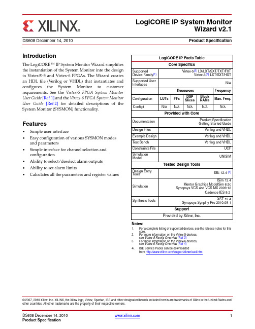
赛灵思(Xilinx)Virtex-5和Virtex-6 FPGA系统监控器向导(LogiCORE
© 2007, 2010 Xilinx, Inc. XILINX, the Xilinx logo, Virtex, Spartan, ISE and other designated brands included herein are trademarks of Xilinx in the United States and other countries. All other trademarks are the property of their respective owners.IntroductionThe LogiCORE™ IP System Monitor Wizard simplifies the instantiation of the System Monitor into the design in Virtex®-5 and Virtex-6 FPGAs. The Wizard creates an HDL file (Verilog or VHDL) that instantiates and configures the System Monitor to customer requirements. See the Virtex-5 FPGA System Monitor User Guide [Ref 1] and the Virtex-6 FPGA System Monitor User Gu ide [Ref 2] for detailed descriptions of the System Monitor (SYSMON) functionality.Features•Simple user interface•Easy configuration of various SYSMON modes and parameters•Simple interface for channel selection and configuration•Ability to select/deselect alarm outputs •Ability to set alarm limits•Calculates all the parameters and register valuesLogiCORE IP System MonitorWizard v2.1DS608 December 14, 2010Product SpecificationLogiCORE IP Facts TableCore SpecificsSupportedDevice Family (1)Virtex-5(2) LX/LXT/SXT/TXT/FXTVirtex-6(3) LXT/SXT/HXTSupported User InterfacesN/AResourcesFrequency Configuration LUTs FFs DSP Slices Block RAMs Max. Freq.Config1N/AN/AN/AN/AN/AProvided with CoreDocumentation Product Specification Getting Started GuideDesign Files Verilog and VHDL Example Design Verilog and VHDL Test Bench Verilog and VHDLConstraints File UCF Simulation ModelUNISIMTested Design ToolsDesign Entry ToolsISE 12.4 (4)SimulationISim 12.4Mentor Graphics ModelSim 6.5c Synopsys VCS and VCS MX 2009.12Cadence IES 9.2Synthesis T oolsXST 12.4Synopsys Synplify Pro 2010.09-1SupportProvided by Xilinx, Inc.Notes:1.For a complete listing of supported devices, see the release notes for this core.2.For more information on the Virtex-5 devices, see Virtex-5 Family Overview [Ref 3]3.For more information on the Virtex-6 devices, see Virtex-6 Family Overview [Ref 4]4.ISE Service Packs can be downloadedfrom /support/download.htmLogiCORE IP System Monitor Wizard v2.1Functional DescriptionThe System Monitor Wizard is an interactive graphical user interface (GUI) that instantiates a SYSMONbased design on specific needs. Using the wizard, users can explicitly configure the SYSMON tooperate in the desired mode. The GUI allows the user to select the channels, enable alarms, and set thealarm limits.SYSMON Functional FeaturesMajor functional SYSMON features can be used to determine an appropriate mode of operation. Thesefeatures include:•Analog to digital conversion•FPGA temperature and voltage monitoring•Generate alarms based on user set parametersI/O SignalsTable1 describes the input and output ports provided from the System Monitor Wizard. Availability ofports is controlled by user-selected parameters. For example, when Dynamic Reconfiguration isselected, these ports are exposed to the user. Any port that is not exposed is appropriately tied off orconnected to a signal labeled unused in the delivered source code.Table 1:System Monitor I/O SignalsPort Direction DescriptionDI_IN[15:0]Input Input data bus for the dynamic reconfiguration port (DRP).DO_OUT[15:0]Output Output data bus for the dynamic reconfiguration port.DADDR_IN[6:0]Input Address bus for the dynamic reconfiguration port.DEN_IN Input Enable signal for the dynamic reconfiguration port.DWE_IN Input Write enable for the dynamic reconfiguration port.DCLK_IN Input Clock input for the dynamic reconfiguration port.DRDY_OUT Output Data ready signal for the dynamic reconfiguration port.RESET_IN Input Reset signal for the System Monitor control logic and max / min registers.CONVST_IN Input Convert start input. This input is used to control the sampling instant on the ADC input and is only used in Event Mode Timing (see Event-Driven Sampling in the Virtex-5 and Virtex-6 FPGA System Monitor user guides, [Ref1] and [Ref2]).CONVSTCLK_IN Input Convert start input. This input is connected to a global clock input on the interconnect. Like CONVST, this input is used to control the sampling instant on the ADC inputs and is only used in Event Mode Timing.VP_IN VN_IN InputOne dedicated analog-input pair. The System Monitor has onepair of dedicated analog-input pins that provide a differentialanalog input.LogiCORE IP System Monitor Wizard v2.1VAUXP15[15:0]VAUXN15[15:0]Inputs16 auxiliary analog-input pairs. In addition to the dedicated differential analog-input, the System Monitor uses 16 differential digital-input pairs as low-bandwidth differential analog inputs. These inputs are configured as analog during FPGA configuration.USER_TEMP_ALARM_OUT Output System Monitor temperature-sensor alarm output.VCCINT_ALARM_OUT Output System Monitor V CCINT -sensor alarm output.VCCAUX_ALARM_OUT Output System Monitor V CCAUX -sensor alarm output.OT_OUTOutput Over-T emperature alarm output.CHANNEL_OUT[4:0]OutputsChannel selection outputs. The ADC input MUX channel selection for the current ADC conversion is placed on these outputs at the end of an ADC conversion.EOC_OUT OutputEnd of Conversion signal. This signal transitions to an active-High at the end of an ADC conversion when the measurement result is written to the status registers. For detailed information, see the System Monitor Timing section in the Virtex-5 and Virtex-6 FPGA System Monitor user guides ([Ref 1] and [Ref 2].)EOS_OUT OutputEnd of Sequence. This signal transitions to an active-High when the measurement data from the last channel in the Channel Sequencer is written to the status registers. For detailed information, see the System Monitor Timing section in the Virtex-5 and Virtex-6 FPGA System Monitor user guides ([Ref 1] and [Ref 2]).BUSY_OUT Output ADC busy signal. This signal transitions High during an ADC conversion. This signal transitions High for an extended period during calibration.JTAGLOCKED_OUT Output Used to indicated that DRP port has been locked by the JTAG interface.JTAGMODIFIED_OUT Output Used to indicate that a JTAG write to the DRP has occurred.JTAGBUSY_OUTOutputUsed to indicate that a JTAG DRP transaction is in progress.Table 1:System Monitor I/O Signals (Cont’d)PortDirection DescriptionLogiCORE IP System Monitor Wizard v2.1User AttributesThe System Monitor functionality is configured through the control registers (See the Register File Interface sections in the Virtex-5 and Virtex-6 FPGA System Monitor user guides: [Ref 1] and [Ref 2]).Table 2 lists the attributes associated with these control registers. These control registers can be initialized when the SYSMON primitive is instantiated in the HDL using the attributes listed in Table 2.The control registers can also be initialized through the DRP at run time. The System Monitor Wizard simplifies the initialization of these control registers in the HDL instantiation. The Wizard will generate the correct bit patterns based on user functionality selected through the Wizard GUI.SupportXilinx provides technical support for this LogiCORE product when used as described in the product documentation. Xilinx cannot guarantee timing, functionality, or support of product if implemented in devices that are not defined in the documentation, if customized beyond that allowed in the product documentation, or if changes are made to any section of the design labeled DO NOT MODIFY .Ordering InformationThe System Monitor™ Wizard LogiCORE IP core is provided free of charge under the terms of the Xilinx End User License Agreement . The core can be generated by the Xilinx ISE CORE Generator software, which is a standard component of the Xilinx ISE Design Suite. This version of the core can be generated using the ISE CORE Generator system v12.4. For more information, please visit the Architecture Wizards web page .Table 2:System Monitor AttributesAttribute Name Control Reg Address DescriptionINIT_40Configuration register 040h System Monitor configuration registers. For detailed information, see the Virtex-5 and Virtex-6 FPGA System Monitor user guides ([Ref 1] and [Ref 2])INIT_41Configuration register 141h INIT_42Configuration register 242hINIT_48 to INIT_4FSequence registers48h to 4Fh Sequence registers used to program the Channel Sequencer function in the System Monitor. Fordetailed information, see the Virtex-5 and Virtex-6FPGA System Monitor user guides ([Ref 1] and [Ref 2]).INIT_50 to INIT_57Alarm Limits registers50h to 57hAlarm threshold registers for the System Monitor alarm function. For detailed information, see theVirtex-5 and Virtex-6 FPGA System Monitor user guides ([Ref 1] and [Ref 2]).SIM_MON ITOR_FILE Simulation Analog Entry File -This is the text file that contains the analog input stimulus. This is used for simulation.SIM_DEVICEDevice family-This is used to identify the device family. This is used for simulation.LogiCORE IP System Monitor Wizard v2.1Information about additional Xilinx LogiCORE modules is available at the Xilinx IP Center . For pricing and availability of other Xilinx LogiCORE modules and software, please contact your local Xilinx sales representative .References1.UG192, Virtex-5 FPGA System Monitor User Guide2.UG370, Virtex-6 FPGA System Monitor User Guide3.DS100, Virtex-5 Family Overview4.DS150, Virtex-6 Family Overview5.UG741, System Monitor Wizard Getting Started GuideRevision HistoryThe following table shows the revision history for this document:Notice of DisclaimerXilinx is providing this product documentation, hereinafter “Information,” to you “AS IS” with no warranty of any kind, express or implied. Xilinx makes no representation that the Information, or any particular implementation thereof, is free from any claims of infringement. You are responsible for obtaining any rights you may require for any implementation based on the Information. All specifications are subject to change without notice. XILINX EXPRESSLY DISCLAIMS ANY WARRANTY WHATSOEVER WITH RESPECT TO THE ADEQUACY OF THE INFORMATION OR ANY IMPLEMENTATION BASED THEREON, INCLUDING BUT NOT LIMITED TO ANY WARRANTIES OR REPRESENTATIONS THAT THIS IMPLEMENTATION IS FREE FROM CLAIMS OF INFRINGEMENT AND ANY IMPLIED WARRANTIES OF MERCHANTABILITY OR FITNESS FOR A PARTICULAR PURPOSE. Except as stated herein, none of the Information may be copied, reproduced,distributed, republished, downloaded, displayed, posted, or transmitted in any form or by any means including,but not limited to, electronic, mechanical, photocopying, recording, or otherwise, without the prior written consent of Xilinx.Date Version Description of Revisions02/15/071.0Initial Xilinx release.04/19/10 2.0LogiCORE IP System Monitor Wizard v2.0 release. Updated tools and version numbers. Expanded supported Virtex-5 devices. Added support for Virtex-5 TXT and FXT sub-families. Added Virtex-6 FPGA support. Added Functional Description , SYSMON Functional Features , I/O Signals , Support , Ordering Information , and References .12/14/10 2.1Updates to the Wizard and tools versions.。
- 1、下载文档前请自行甄别文档内容的完整性,平台不提供额外的编辑、内容补充、找答案等附加服务。
- 2、"仅部分预览"的文档,不可在线预览部分如存在完整性等问题,可反馈申请退款(可完整预览的文档不适用该条件!)。
- 3、如文档侵犯您的权益,请联系客服反馈,我们会尽快为您处理(人工客服工作时间:9:00-18:30)。
赛灵思官网资源导读俗话说“授之鱼不如授之以渔”,看到这边有人要资料有人送资料的,其实论坛不更应该是一个交流的空间么?那就让找资料更有效率一点,让大家花更多时间来交流吧。
言归正传,写这篇文章主要想介绍Xilinx各种资料的找法、分类方法和什么问题该看哪些资料。
限于经验,难免有错漏,希望大家指出错误并继续补充。
一、软件Xilinx的软件主要是ISE, EDK, ChipScope Pro, System Generator, PlanAhead, ModelSim,如果要算上AccelDSP也凑合,不过相信国内没多少人用。
ISE是主要的逻辑设计软件,其他软件的具体实现功能都依附于ISE。
ISE有Foundation版和WebPack版。
WebPack版免费,Foundation版收费。
两者的区别是支持的器件不同。
功能是相同的。
WebPack版支持的功能可以看/blog/link2url.php?link=http%3A%2F%%2Fise%2Fpro ducts%2Fwebpack_config.htm。
Foundation的话当然全支持拉,要看的话在这里/blog/link2url.php?link=http%3A%2F%%2Fise%2Flogi c_design_prod%2Ffoundation.htm。
说这些的目的就是,如果你的器件WebPack支持,就直接到网上下载WebPack吧,没有版权之类的后顾之忧;如果不行,Verycd上找些东西还是挺方便的。
ModelSim MX有免费的starter version,可以和ISE WebPack一起下载,安装以后在开始里面点licens_e request就可以申请starter的使用权了。
另外,可以VHDL和Verilog各申请一个,那么就可以仿真两种语言了,不过不支持mix language。
/blog/link2url.php?link=http%3A%2F%%2Fise%2Fverifica tion%2Fmxe_details.html不过那一页说的ModelSim XE的use case不准的,XE,PE,SE的差别还是仔细看这里吧。
/blog/link2url.php?link=http%3A%2F%%2Fxlnx%2Fxil_an s_display.jsp%3FgetPagePath%3D24506ChipScope是片内的逻辑分析仪,可以让用户方便地抓取片内信号进行debug。
ChipScope有60天的评估版。
/blog/link2url.php?link=http%3A%2F%%2FchipscopePlanAhead(稍微介绍下子,没有接触过的朋友可能不知道这是什么)PlanAhead是ISE7以后推出的软件,它的主要功能是对一个综合后的NGC/EDIF网表进行布局布线的规划。
听上去功能有点像FloorPlanner,但是功能却强大得多。
罗列一下我喜欢它的地方:1、因为使用了GateVision的EDIF显示引擎,使综合网表显示非常漂亮。
2、ExplorerAhead可以控制具体使用哪些MAP/PAR的参数,比使用Xplorer更方便,提高Timing 结果很有效率,还支持多CPU。
3、Show Hierarchy可以看出每个层次的连接以及每个层次占地大小的比例。
4、画Pblock,规划布局布线。
这个就有点像FloorPlanner,但是可以显示每个画出的Pblock包括多少资源,并可以仅对某个Pblock布局布线,布局后还能整体移动整个Pblock。
5、自带的Tutorial很周到,容易上手。
以上是我用过的功能,还没用过的功能是:1、PinAhead自动检查DRC和WASSO,自动放Pin。
2、用PlanAhead做Partial Reconfiguration,流程比以前方便很多很多。
PlanAhead有30天的免费评估版。
曾经可以30天试用期过后再申请一次评估版,但现在随着PlanAhead的日渐成熟和广受好评,再次试用的功能已经取消了。
/blog/link2url.php?link=http%3A%2F%%2Fplanahead以上这些工具是通常做一些HDL代码开发/实现是所需要使用到的工具,除了这些,Xilinx还提供有EDK和System Generator这些已经将部分功能模块化,让用户方便得点几下鼠标就可以建立起一个基本系统,并在此基础上再次开发的工具。
EDK - Embedded Development Kit,顾名思义就是用来做嵌入式系统的。
它提供对PowerPC硬核和MicroBlaze软核的支持,免费提供一些常用的硬件IP Core,比如各种Memory Controller、各种外设如IIC, SPI, GPIO,并集成了GNU工具链,使之成为软硬件设计一体化的设计工具。
设计出的嵌入式系统集标准性与灵活性于一身,可以支持Linux等操作系统,也可让用户自己设计用户IP用作模块接口或硬件加速。
/blog/link2url.php?link=http%3A%2F%%2FedkSystem Generator借助Matlab Simulink的框架使DSP算法用图形化的数据流来说明,在Sysgen 的帮助下DSP算法可以轻易在FPGA上实现。
特别是它的Hardware Co-simulation功能大大降低了Debug的难度。
/blog/link2url.php?link=http%3A%2F%%2Fsysgen二、软件更新/blog/link2url.php?link=http%3A%2F%%2Fdownload是Xilinx的Download Center,ISE的Service Pack, IP Update在那里都有下。
现在Download Center 里的Service Pack和IP Update等软件更新不用注册帐号就可以下载了。
关于更新,多说两句。
不管正在使用ISE的哪个版本,出了新的Service Pack就及时下载更新一下,这样会省去你很多可能会有的麻烦。
一般Service Pack 1在公开发布的主要版本的3天后就会发布,而后的每个Service Pack都相隔一个月左右。
ISE Service Pack是指ISE除了CoreGen和IP Core以外的所有更新;IP Update当然就指CoreGen 和IP Core的更新了。
IP Update打上了以后,用ModelSim XE的要下载XE的更新的库,用SE或者PE的要用compxlib 重新编译一下库。
有一个东西可能不是很多人用,就是Download Center里的CAE Vendor Library。
里面是给第三方软件使用的库,比如Cadence/Synopsys的综合工具、形式验证工具等。
Download Center中一般只显示每个版本的最新的Service Pack,比如ISE 9.1只能找到Service Pack 3,而找不到SP2,那是因为SP3已经包含了所有SP2的更新。
但是如果有特定需要,也可以在以下这些Answer Record中找到特定版本的Service Pack:AR #10959 - ISE Install - Where can I find and download old service packs for ISE?AR #31741 - ISE Install - Where can I find and download old ip updates for ISE?AR #25399 - EDK Install - Where can I find and download old service packs for EDK?三、软件教程作为入门教程来说,Xilinx放在Demosondemond网站上的那些视频教程可以说是最好的了。
链接就在Xilinx主页左下角的位置。
/blog/link2url.php?link=http%3A%2F%%2Fcli ents%2Fxilinx%2F001%2Fpage%2Findex.asp视频教程内容有关于最新的硬件的,也有各种软件的,基本算挺齐全的。
有多好,自己看就知道了:)最近要查看demosondemand网站的录像需要注册了,dod的注册很严格,注册需要公司邮件地址或者学校带edu的邮件地址。
视频资料还有一类,就是放在TechOnline上的WebCast。
涉及面不止软件,也还有很多硬件的资料。
alex_yyp总结得很好,我抄一下嘿嘿:/blog/link2url.php?link=http%3A%2F%%2Felec tronics_directory%2Fwebinar%2F896WebCast都是可以与演讲者实时互动的(虽然大多是美国的,时区跟我们有差异,但是中国的WebCast也还是有的),最新的WebCast信息可以订阅TechOnline,或者在的网站右上角察看。
接下来应该看的是Tutorial。
/blog/link2url.php?link=http%3A%2F%%2Fsupport%2Fte chsup%2Ftutorials%2F主要是ISE, EDK, PlanAhead的,还有Timing Constraint的。
时序约束的那篇文档算是讲得比较全的,还有可以深入阅读的一篇文档就是wp237,关于offset约束的。
ISE做了Tutorial基本操作应该没问题了。
ChipScope比较简单看了Demosondemond的视频教程应该就会了。
还不清楚的话看看安装目录里的UG029。
PlanAhead虽然比ChipScope复杂,但是视频教程还是很不错的,再加上Tutorial,应该也够了。
更进阶了解ISE,需要阅读ISE的Manual。
打开Manual可以从开始菜单中ISE->Documentation->Software Manuals;也可以在ISE安装目录下的doc目录查找。
列出几个重要的Manual:XST User Guide (xst.pdf):关于XST的开关选项等Development System Reference Guide (dev.pdf) :除了XST外的实现工具比如map, par, trce等的实用指南Constraint Guide (cgd.pdf) :约束的指南。
包括时序约束/非时序约束;UCF约束/XCF约束。
Synthesis and Simulation Guide (sim.pdf):其实主要是说明仿真的具体内容。