
xilinx的Chipscope的使用方法
Chipscope的使用方法首先插入chipscope核,在以下路径打开:
然后加载工程的NGC文件:
加载完之后,选择NEXT。
继续next。
这里要选择Trigger的宽度,最大是256,我们一般选择256,以后用多少再返回来修改。
剩下的2项的选择,如下:
然后选择modify connections,
首先选择工程的主时钟,
在选择想要抓取的信号,
选择完后,如果所用的CH少于256,则需要返回之前的地方修改一下,
当所有的信号添加完成后,我们选择insert,加入chipscope核到工程中。
此时,ISE会重新跑一遍synthesize(综合),当执行完后,会产生下面蓝色的信息。
此时,在ISE中执行implement,点击run。
然后,记得保存chipscope,
会保存为.CDC文件,我这里命名保存的是test.cdc。
然后生成bit文件。
这样chipscope核就添加好了。
然后打开ISE中的analyze design using chipscope。
或者这样打开也行,如图:
然后选择连接V6平台,
然后配置V6平台,
选择bit和cdc文件,
这样点击OK,ISE会重新下载一遍工程,然后点击T!,就可以看到需要的信号数据了。
点击这个地方你可以看到想看到的选项,
BUS Plot选项是可以看到数据的波形的,waveform可以看到数据。
Trigger setup是设置触发条件和执行触发的,listing暂时不知道干嘛用的。
ISE10.1使用教程简介
ISE 10.1Steps1 new project (1)2 new source (3)3 run behavior simulation (5)4 ChipScope (7)5 Constraints (12)6 synthesize your design (13)7 implement your design (13)8 Generate Programming File (13)9Analyze Design Using Chipscope (13)1 new project1. 双击桌面Xilinx ISE10.1 快捷方式打开ISE 工程管理器(Project Navigator)。
2. 打开 Project Navigator 后,选择File → New Project ,弹出新建工程对话框,填写工程名字,工程存放发热位置。
注意,不要填写含有中文的名字,以免发生错误。
3.点击 Next 按钮,弹出器件特性对话框。
Device Family选择“Virtex2P”,Device选“XC2VP30 ,Package选择ff896,Speed选 -7”,其他选择如下图所示。
其中这些选择由按FPGA开发板的型号来决定的。
然后点击NEXT,继续单击Next 按钮,然后单击Finish按钮完成对工程的建立和基本设置。
2 new source1在工程的Source for下在的空白处单击右键选择New Source菜单2然后在弹出的对话框中选择Verilog Module,并且在右边的File name中输入你的模块名称,然后单击Next按钮。
2.这是一个设置输入输出端口的对话框,可以设置,也可以不设置。
一般选择不设置,直接点击NEXT,最后单击Finish按钮完成成对Verilog Module模块资源的添加。
3.双击Source for下面的.v文件(本实验双击counter.v)进入源代码编辑框中,并在里面编写Verilog源程序,然后点击保存按钮。
ChipScope Pro详细教程(Xilinx在线逻辑分析仪)
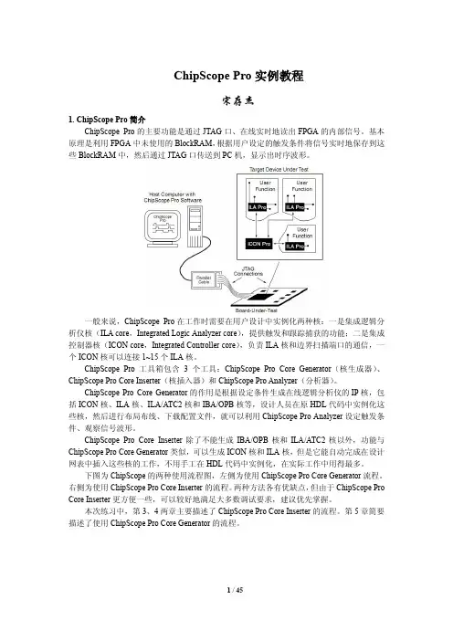
ChipScope Pro实例教程宋存杰1. ChipScope Pro简介ChipScope Pro的主要功能是通过JTAG口、在线实时地读出FPGA的内部信号。
基本原理是利用FPGA中未使用的BlockRAM,根据用户设定的触发条件将信号实时地保存到这些BlockRAM中,然后通过JTAG口传送到PC机,显示出时序波形。
一般来说,ChipScope Pro在工作时需要在用户设计中实例化两种核:一是集成逻辑分析仪核(ILA core,Integrated Logic Analyzer core),提供触发和跟踪捕获的功能;二是集成控制器核(ICON core,Integrated Controller core),负责ILA核和边界扫描端口的通信,一个ICON核可以连接1~15个ILA核。
ChipScope Pro工具箱包含3个工具:ChipScope Pro Core Generator(核生成器)、ChipScope Pro Core Inserter(核插入器)和ChipScope Pro Analyzer(分析器)。
ChipScope Pro Core Generator的作用是根据设定条件生成在线逻辑分析仪的IP核,包括ICON核、ILA核、ILA/ATC2核和IBA/OPB核等,设计人员在原HDL代码中实例化这些核,然后进行布局布线、下载配置文件,就可以利用ChipScope Pro Analyzer设定触发条件、观察信号波形。
ChipScope Pro Core Inserter除了不能生成IBA/OPB核和ILA/ATC2核以外,功能与ChipScope Pro Core Generator类似,可以生成ICON核和ILA核,但是它能自动完成在设计网表中插入这些核的工作,不用手工在HDL代码中实例化,在实际工作中用得最多。
下图为ChipScope的两种使用流程图,左侧为使用ChipScope Pro Core Generator流程。
片内逻辑分析仪工具——ChipScopePro

第11章片内逻辑分析仪工具——ChipScope Pro11.1 ChipScope Pro工具介绍在FPGA调试阶段,传统的信号分析手段要求在设计时保留一定数量的FPGA管脚作为测试管脚,这种方法灵活性差,对PCB布线也有一定的影响。
当今先进的FPGA器件所具有的规模、速度和板级要求使得利用传统逻辑分析方法来调试采用FPGA器件进行的设计几乎是不可能的。
Xilinx公司推出的片内逻辑分析仪ChipScope Pro能够通过JTAG口,实时地读出FPGA的所有内部信号,而只需要片内的少量BlockRAM和逻辑资源,使得逻辑分析灵活方便。
ChipScope Pro是与ISE配套使用的,其版本经过了ChipScope 4.1i,ChipScope 4.2i,ChipScope Pro 5.1i,ChipScope Pro 5.2i和ChipScope Pro 6.1i的升级过程,ChipScope Pro 6.1i是与ISE 6.1配套使用的最新版本。
ChipScope Pro软件由3个工具组成:(1) ChipScope Pro内核生成器:为综合控制器(ICON)内核、CoreConnect™ OPB的总线分析内核(IBA/OPB)、逻辑分析(ILA)内核及安捷伦跟踪内核(ILA/ATC)提供网表和实例化的模板;(2) ChipScope Pro内核插入器:自动地为用户已经综合完的设计中插入ICON、ILA和ILA/ATC的内核;(3) ChipScope Pro分析仪:提供器件的配置、触发的设定和ILA、IBA/OPB及ILA/ATC核的踪迹显示功能。
各种内核实现了信号的触发和捕获,而ICON内核专门用于与边界扫描(Boundary Scan)管脚的通信。
使用ChipScope Pro工具的设计可以容易地同任何标准的FPGA设计流程结合起来,其中要用到标准的HDL综合工具和Xilinx ISE的实现工具,设计流程如图11.1所示。
MB使用心得
今天在网上的高人(青芷蓝烟)指点,用chipscope调试MB,不过到目前(2006-3-27 17:17pm)还没有搞出来。
青芷蓝烟(30840814) 16:47:50我的意思是,EDK中不要那个chipscope的核和mdm 而是将它的project option 设为submode 将它Export to ProjNav青芷蓝烟(30840814) 16:48:19在那里新建一个cdc 文件,调用chipscope海洋深处~(4704295) 16:55:53export to Projnav 是什么啊,弄到ISE里面?青芷蓝烟(30840814) 16:49:01就是完全和在ISE中使用chipscope 一样青芷蓝烟(30840814) 16:49:17你看你的option 选项海洋深处~(4704295) 16:56:35哦青芷蓝烟(30840814) 16:49:37里面有project options青芷蓝烟(30840814) 16:50:04打开就可以看到可以设置你的project是top mode haishi sub mode海洋深处~(4704295) 16:57:44哦,这里有选项青芷蓝烟(30840814) 16:50:56你把它设为submode青芷蓝烟(30840814) 16:51:07然后生成网表海洋深处~(4704295) 16:58:11嗯,设了海洋深处~(4704295) 16:58:14哦青芷蓝烟(30840814) 16:51:37再在Tools->Export to ProjNav海洋深处~(4704295) 16:59:00哦海洋深处~(4704295) 16:59:19这些是哪里看到的哦,自己领悟的?青芷蓝烟(30840814) 16:53:19这个是某个指南上有的应该就在EDK->doc 里青芷蓝烟(30840814) 16:53:43也许是system tools 指南,也许是XPS 指南,忘了:)海洋深处~(4704295) 17:00:56哦海洋深处~(4704295) 17:01:07我太着急了,没有看海洋深处~(4704295) 17:01:10来不及看海洋深处~(4704295) 17:01:12唉。
ChipScope使用方法说明

ChipScope使用方法说明拟制李雷鸣日期2005-6-41 ChipScope简介ChipScope的主要功能是能通过JTAG口,在线、实时地读出FPGA内部逻辑的任何信号。
其基本原理是利用FPGA中未使用的Block Ram,将想要观察的信号(寄存器,网线)实时地存到这些BlockRam中,然后根据用户设定的触发条件生成特定的地址译码选择数据读出,送到JTAG口,然后在计算机中根据这些数据动态地画出时序波形来。
使用ChipScope分析FPGA内部信号的优点如下:1. 成本低廉,只要有这套软件加上一根JTAG电缆就可完成信号的分析。
2. 灵活性大,可观测信号的数量和存储深度仅由器件剩余的Block Ram数量决定。
剩余Block Ram越多,可分析的信号的数量和存储深度就越大。
3. 使用方便,该软件可以自动读取原设计生成的网表(*.ngc,*.edf,*.edn)区分时钟信号和普通信号,待观测信号的设定也十分方便,存储深度可变。
可以设计多种触发条件的组合。
然后软件自动将其IP核的网表插入到原设计的网表中。
其IP核只使用少量的查找表资源和寄存器资源,对原设计的影响很小。
4. 使FPGA不再是“黑箱”。
Chip Scope 可以十分方便的观测FPGA内部的所有信号,包括寄存器,网线型,甚至可以观测综合器产生的重命名的连接信号,使FPGA不再是“黑箱”,对FPGA内部逻辑调试非常方便。
2 ChipScope组成ChipScope工具箱包含三个工具:ChipScope Core Generator, ChipScope Core Inserter,和ChipScope Analyzer。
ChipScope Core Generator的作用是根据设定条件生成在线逻辑分析仪的IP核。
使用方法和Xilinx的Core Generator相似。
ChipScope Core Inserter完成读取并分析原设计的网表,设置待分析信号,设定触发条件,和自动生成的该在线逻辑分析仪lP核的网表,并将网表插入到原设计的网表中去。
ISE中chipscope的使用

ChipScope Debug LabIntroductionThis lab guides you through the process of inserting ChipScope-Pro cores into your design and performing on-chip verification.ObjectivesAfter completing this lab, you will be able to:• Create a new ChipScope-Pro source in ISE• Create ILA and ICON cores using ChipScope-Pro and insert it into a PicoBlaze design • Specify trigger options in ChipScope Analyzer• Download the bitstream and run the design in hardware• Perform an on-chip verification and view the wave forms in ChipScope AnalyzerDesign DescriptionYou will extend the lab 5 design by adding a ChipScope ILA core to the PicoBlaze output bus. Next, you will setup the trigger to capture data when text is entered via Hyper Terminal. You should see the resulting text displayed in ChipScope when the buffer is full.ProcedureThis lab is separated into steps that consist of general overview statements that provide information on the detailed instructions that follow. Follow these detailed instructions to progress through the lab. This lab comprises 4 primary steps: You will create a new ChipScope source, configure and connect an ILA core, configure ChipScope Analyzer trigger options and, finally, perform an on-chip verification. Note: If you are unable to complete the lab at this time, you can download the lab files for this module from the Xilinx University Program site at /universityGeneral Flow for this LabStep 1:Creating a New ChipScope SourceStep 2: Configure and Connect an ILA Core Step 3:Configure ChipScope Analyzer Trigger OptionsStep 4: Perform an On-chip VerificationCreate a New ChipScope Source Step 1 1-1. Open a ChipScope-Pro project from lab6 folder (under vhdl or verilog).1-1-1. Open the Xilinx ISE software by selecting Start All Programs Xilinx ISE Design Suite13.2 ISE Design Tools Project Navigator.1-1-2. Open the project by selecting File Open Project.○Verilog users: Browse to c:\xup\fpgaflow\labs\verilog\lab6\chipccope○VHDL users: Browse to c:\xup\fpgaflow\labs\vhdl\lab6\chipscope1-1-3. Select chipscope.xise and click Open.1-1-4. Create a new ChipScope Definition and Connection File source by selecting Project New Source and entering the name loopback_cs. Click Next to continue.Figure 1. New Source Dialog Box1-1-5. Click Finish. A ChipScope-Pro source will be added to the Sources in Project window.Genesys 6-2 /universityFigure 2. ChipScope Definition and Connection (.cdc) added to VHDL ProjectConfigure and Connect an ILA Core Step 2 2-1. Connect the ILA core to the PicoBlaze output.2-1-1. Double-click the loopback_cs.cdc file in the sources in project window to open the core inserter project.Figure 3. ChipScope-Pro Core InserterNote: Projects saved in the Core Inserter hold all relevant information about source files, destination files, core parameters and core settings.2-1-2. Click Next and then click New ILA Unit. Notice in the left hand window how an instance of the ILA core, U0:ILA, is added to the system.Genesys 6-4 /universityFigure 4. Insert a new integrated logic analyzer (ILA) Unit2-1-3. Click Next to setup the trigger parameters.Each ILA or ILA/ATC core can have up to 16 separate trigger ports that can be setup independently. The individual trigger ports are buses that are made up of individual signals or bits that can range from 1 to 256 bits. Each trigger port can be connected to 1 to 16 match units. A match unit is a comparator that is connected to a trigger port and is used to detect events on that trigger port. The results of one or more match units are combined together to form the overall trigger condition event that is used to control the capturing of data. The different comparisons or match functions that can be performed by the trigger port match units depend on the type of match unit. The ILA and ILA/ITC cores support six types of match units. In this lab, you will setup the ILA core to trigger via some UART control signals.2-1-4. Set the following ILA trigger parameters as follows and then click Next.Trigger Input and Match Unit Settings.• Number of input trigger ports: 3Trigger Port Trigger Width # Match Units Counter WidthMatch Type TRIG0 1 1 Disabled Basic TRIG1 1 1 Disabled Basic TRIG211DisabledBasicTrigger Condition Settings• Enable Trigger Sequencer: Checked (This allows you to specify a sequence of events to enable triggering)•Max Number of Sequencer Levels: 2Storage Qualification Condition Settings• Enable Storage Qualification: Checked (This allows you to specify which data will be stored in the internal buffer)Figure 5. Specify the Trigger ParametersThe maximum number of data sample words that the ILA core can store in the sample buffer is called the data depth. The data depth determines the number of data width bits contributed by each block RAM unit used by the ILA unit. The maximum number of data sample words that can be captured depends on the number and size of block RAM, which varies according to device family and density.2-1-5. Set the following capture parameters and click Next.• Data Depth: 1024• Sample On: Rising clock edge• Data Same as Trigger Port: unchecked• Data Width: 8Figure 6. Specify Trigger ParametersThe net connections tab allows you to choose the signals to connect to the ILA core. If trigger is separate from data, then clock, trigger, and data must be specified. Connections that have not been made will appear in red.Figure 7. Unconnected Net Connections2-1-6. Click the Modify Connections tab.Figure 8. Net ConnectionsThe Select Net dialog provides an easy interface to choose nets to connect to the ILA, ILA/ATC or ATC2 cores. The hierarchical structure of the design can be traversed using the Structure/Nets pane. All the design’s nets of the selected structure hierarchy appear in the table at the lower left pane. The Clock Signals and Trigger/Data Signals tabs illustrate the net connections between the design and the ILA core.2-1-7. With the Clock Signals tab under Net Selections selected, highlight the entry for clk55MHz in the listing of nets and click the Make Connections button to connect the clock signal in the design to the clock port of the ILA core.Figure 9. Connect the clockGenesys 6-6 /university2-1-8. Click the Trigger Signals tab, and connect the three trigger ports as follows:• TP0: data_present (this signal indicates that data is present in the uart_rx module• TP1: read_from_uart (input to uart_rx that indicates that a read operation will occur)• TP2: write_to_uart (input to uart_tx that indicates that a write operation will occur)2-1-9. Click the Data Signals tab and connect the output port of the PicoBlaze controller to the data port of the ILA core (see Figure 10), and click OK.Figure 10. Connect the PicoBlaze output port2-1-10. You will notice that the Clock, Trigger, and Data ports under Net Connections are highlighted in black, indicating valid connections. Click Return to Project Navigator and save the file.Figure 11. Connection between Design and ILA core EstablishedConfigure ChipScope Analyzer Trigger Options Step 3 3-1. You will download the bitstream using ChipScope and configure the ILA core to trigger when the UART reads text from Hyper Terminal.3-1-1. With the top-level file (loopback.v/vhd) selected, double-click on Analyze Design Using ChipScope in the Processes window.3-1-2. Connect up the download cable and power up the Genesys board.3-1-3. Click the Open Cable/Search JTAG Chain button.Figure 12. Establish JTAG Connection3-1-4. Chipscope Pro Analyzer will automatically detect the devices on the Genesys board and then click OK.Figure 13. Impact Detects Devices in JTAG Chain3-1-5. Right Click on the xc5vlx50t device and select configure.3-1-6. Click Select New File and select the loopback.bit bitstream file from the project directory. Note that the import cdc file field shows the cdc file located in the project directory. Also note that the tool will create a bus (out_port) automatically. Click OK.Double-click on Trigger Setup and Waveform entries in Project Tree to open the respective windows.The ChipScope Pro Analyzer interface consists of four parts:Genesys 6-8 /universityFigure 14. ChipScope Analyzer WindowEach ChipScope Pro ILA, ILA/ATC, and IBA core has its own Trigger setup window, which provides a graphical interface for the user to setup triggers. The trigger mechanism inside each ChipScope Pro core can be modified at run-time without having to recompile the design. There are three components to the trigger mechanism:• Match Functions: Defines the match or comparison value of each match unit• Trigger Conditions: Defines the overall trigger condition based on a binary equation or sequence of one or more match functions• Capture Settings: Defines how many samples to capture, how many capture windows, and the position of the trigger in those windowsIn this design, you will setup the triggers to capture text at the PicoBlaze output port, after being entered via Hyper Terminal.3-1-7. Specify the Match Units as follows:• M0:TriggerPort0 (data_present): Value 1• M1:TriggerPort1(read_from_uart): Value 1• M2:TriggerPort1(write_to_uart): Value 1Figure 15. Setup the Match Units3-1-8. Click the field under Trigger Condition Equation, set the equation M0 M1 in the Sequencertab, and then click OK.Genesys 6-10 /universityFigure 16. Trigger Condition Equation3-1-9. Check the field next to Storage Qualification , select the AND Equation , and check M2. ClickOK . This will enable the ILA core to capture data in the buffer only when data is present, and not on every single clock edge.Figure 17. Storage Qualification EquationPerform an On-Chip VerificationStep 44-1.Start Hyper-Terminal program. Set baud rate to 9600. Arm the trigger and view the waveforms of the captured data.4-1-1.Start the Hyper-Terminal program. Make sure that the baud rate is set to 9600.Lab WorkbookChipScope Debug Lab/university Genesys 6-11xup@4-1-2. Set the buffer depth to 16.Figure 18. Select Buffer Depth4-1-3. Cick the Apply Settings and Arm Trigger button.Figure 19. Apply Settings and Arm Trigger4-1-4. Type “Xilinx #1 FPGA!” in Hyper Terminal and view the message in ChipScope Analyzer.Figure 20. Output in Waveform Window4-1-5. Close all applications without saving ChipScope project.ConclusionYou inserted the ILA and ICON cores into the PicoBlaze design, set up trigger conditions in ChipScope Analyzer, performed an on-chip verification, and analyzed the waveforms in ChipScope-Pro Analyzer.。
Xilinx手册
Xilinx® Virtex™-5 FXT Evaluation KitUser GuideTable of Contents1.0Introduction (4)1.1Description (4)1.2Board Features (4)1.3Test Files (4)1.4Reference Designs (5)1.5Ordering Information (5)2.0Functional Description (6)2.1Xilinx Virtex-5 FX30T FPGA (6)2.2Memory (6)2.2.1DDR2 SDRAM Interface (7)2.2.2Flash Memory (10)2.3Clock Sources (10)2.4Communication (12)2.4.1.110/100/1000 Ethernet PHY (12)2.4.1.2Universal Serial Bus (USB) to UART Bridge Transceiver (14)2.4.1.3RS232 (14)2.5User Switches (15)2.6User LEDs (16)2.7Configuration and Debug Ports (16)2.7.1Configuration Modes (16)2.7.2System ACE™ Module Connector (17)2.7.3JTAG Port (PC4) (18)2.7.4CPU Debug Port (19)2.7.5CPU Trace Port (19)2.8Power (20)2.8.1FPGA I/O Voltage (Vcco) (20)2.8.2FPGA Reference Voltage (Vref) (21)2.9Expansion Connectors (21)2.9.1EXP Interface (21)3.0Test Designs (24)3.1Factory Test (24)3.2Ethernet Test (24)3.3USB UART Test (24)4.0Revisions (25)Appendix A (26)FiguresFigure 1 - Virtex-5 FXT Evaluation Board Picture (5)Figure 2 - Virtex-5 FXT Evaluation Board Block Diagram (6)Figure 3 - Virtex-5 FXT Evaluation Board Memory Interfaces (7)Figure 4 - DDR2 SDRAM Interface (7)Figure 5 - Clock Nets Connected to Global Clock Inputs (11)Figure 6 - 10/100/1000 Mb/s Ethernet Interface (12)Figure 7 - USB to UART Transceiver Interface (14)Figure 8 - RS232 Interface (15)Figure 9 - SAM Interface (50-pin header) (17)Figure 10 - PC4 JTAG Port Connector (18)Figure 11 - CPU Debug Connector (19)Figure 12 - CPU Trace Connector (19)Figure 13 – Virtex-5 FXT Evaluation Board Power (20)Figure 14 - EXP I/O Voltage Jumpers (21)Figure 15 - Virtex-5 FXT Evaluation Board Placement (26)TablesTable 1 - Ordering Information (5)Table 2 - XC5FX30T Features (6)Table 3 - DDR2 SDRAM Timing Parameters (8)Table 4 - Virtex-5 FXT DDR2 FPGA Pinouts (9)Table 5 - Virtex-5 Flash Memory Pinout (10)Table 6 - On-Board Clock Sources (11)Table 7 - Clock Socket "U12" Pin-out (11)Table 8 - User Clock Input (12)Table 9 - Ethernet PHY Hardware Strapping Options (13)Table 10 - Ethernet PHY Pin Assignments (14)Table 11 - USB to UART Interface FPGA Pin-out (14)Table 12 - RS232 Signals (15)Table 13 - Push-Button Pin Assignments (15)Table 14 - DIP Switch Pin Assignments (16)Table 15 - LED Pin Assignments (16)Table 16 - FPGA Configuration Modes (16)Table 17 - SAM Interface Signals (18)Table 18 - V5FX30T I/O Bank Voltages (20)Table 19 - EXP Connector Signals (22)Table 20 - EXP Connector "JX1" Pin-out (23)1.0 IntroductionThe purpose of this manual is to describe the functionality and contents of the Virtex-5 FXT Evaluation Kit from Avnet Electronics Marketing. This document includes instructions for operating the board, descriptions of the hardware features and explanations of the test code programmed in the on-board flash.1.1 DescriptionThe Virtex-5 FXT Evaluation Kit provides a complete hardware environment for designers to accelerate their time to market.The kit delivers a stable platform to develop and test designs targeted to the advanced Xilinx FPGA family. The installed Virtex-5 FX30T device offers a prototyping environment to effectively demonstrate the enhanced benefits of leading edge Xilinx FPGA solutions. Reference designs are included with the kit to exercise standard peripherals on the development board for a quick start to device familiarization.Features1.2 BoardFPGA— Xilinx Virtex-5 XC5VFX30T-FF665 FPGAI/O Connectors— One EXP general-purpose I/O expansion connectors— One 50-pin 0.1” Header supports Avnet System ACE Module (SAM)— 16-pin 0.1” CPU debug header— Mictor CPU Trace Port— User Clock Inputs via Differential SMA ConnectorsMemory— 64 MB DDR2 SDRAM— 16 MB FLASHCommunication— RS-232 serial port— USB-RS232 Port— 10/100/1000 Ethernet PHYPower— Regulated 3.3V, 2.5V, and 1.0V supply voltages derived from an external 5V supply— DDR2 termination (0.9V) and supply/reference voltage (1.8V) regulator.Configuration— Xilinx Parallel Cable IV or Platform USB Cable support for JTAG Programming/Configuration— 16MB Intel BPI FlashFiles1.3 TestThe flash memory on the Virtex-5 FX30T Evaluation Board comes programmed with a factory test design that can be used as base tests for some of the peripherals on the board. The test designs listed below are discussed in Section 3.0. The factory test will test the following interfaces/peripherals:— DDR2 memory— Flash memory— User LEDs— User push-buttonsOther factory test designs for testing the Ethernet and USB-RS232 interfaces are available on the Avnet Design Resource Center web site (/drc).1.4 ReferenceDesignsReference designs that demonstrate some of the potential applications of the board can be downloaded from the Avnet Design Resource Center (/drc). The reference designs include all of the source code and project files necessary to implement the designs. See the PDF document included with each reference design for a complete description of the design and detailed instructions for running a demonstration on the evaluation board. Check the DRC periodically for updates and new designs.Figure 1 - Virtex-5 FXT Evaluation Board Picture1.5 OrderingInformationThe following table lists the development kit part number.Internet link at /drcPart Number HardwareAES-V5FXT-EVL30-G Xilinx Virtex-5 FXT Kit populated with an XC5VFX30T-1 speed grade deviceTable 1 - Ordering Information2.0 Functional DescriptionA high-level block diagram of the Virtex-5 FXT Evaluation board is shown below followed by a brief description of each sub-section.Figure 2 - Virtex-5 FXT Evaluation Board Block Diagram2.1 Xilinx Virtex-5 FX30T FPGAThe Virtex-5 FX30T FPGA features 4 DCMs, 2 PLLs, and 1.25 Gbps LVDS I/O. The following table shows some other main features of the FF676 package.Device Number ofSlices BlockRAM(Kb)DSP48ESlicesXC5VFX30T 5,120 2,448 64Table 2 - XC5FX30T FeaturesPlease refer to the Virtex-5 FX30T Data sheet for a complete detailed summary of all device features.324 of the 360 available I/O on the Virtex-5 FX30T device are used in the design.2.2 MemoryThe Virtex-5 FXT Evaluation Board is populated with both high-speed RAM and non-volatile Flash to support various types of applications. The board has 64 Megabytes (MB) of DDR2 SDRAM and 16 MB of Flash. The following figure shows a high-level block diagram of the memory interfaces on the evaluation board. If additional memory is necessary for development, check the Avnet Design Resource Center (DRC) for the availability of EXP compliant daughter cards with expansion memory (sold separately). Here is the link to the DRC web page: /drc.Figure 3 - Virtex-5 FXT Evaluation Board Memory Interfaces2.2.1 DDR2 SDRAM InterfaceTwo Micron DDR2 SDRAM devices, part number MT47H16M16BG-5E, make up the 32-bit data bus. Each device provides 32MB of memory on a single IC and is organized as 4 Megabits x 16 x 4 banks (256 Megabit). The device has an operating voltage of 1.8V and the interface is JEDEC Standard SSTL_2 (Class I for unidirectional signals, Class II for bidirectional signals). The -5E speed grade supports 5 ns cycle times with a 3 clock read latency (DDR2-400). DDR2 On-Die-Termination (ODT) is also supported. The following figure shows a high-level block diagram of the DDR SDRAM interface on the Virtex-5 FXT Evaluation Board.Figure 4 - DDR2 SDRAM InterfaceThe following table provides timing and other information about the Micron device necessary to implement a DDR2 memory controller.MT47H16M16BG-5E: Timing Parameters Time (ps) orNumberLoad Mode Register time (TMRD) 25000Write Recovery time (TWR) 15000Write-to-Read Command Delay (TWTR) 1Delay between ACT and PRE Commands (TRAS) 90000Delay after ACT before another ACT (TRC) 65000Delay after AUTOREFRESH Command (TRFC) 115000Delay after ACT before READ/WRITE (TRCD) 25000Delay after ACT before another row ACT (TRRD) 15000Delay after PRECHARGE Command (TRP) 20000Refresh Command Interval (TREFC) 115000Avg. Refresh Period (TREFI) 7800000Memory Data Width (DWIDTH) (x2 devices) 32Row Address Width (AWIDTH) 13Column Address Width (COL_AWIDTH) 9Bank Address Width (BANK_AWIDTH) 2Memory Range (64 MB total) 0x3FFFFFFTable 3 - DDR2 SDRAM Timing ParametersThe following guidelines were used in the design of the DDR2 interface to the Virtex-5 FX30T FPGA. These guidelines are based on Micron recommendations and board level simulation.•Dedicated bus with matched trace lengths (+/- 100 mils)•Memory clocks routed differentially•50 ohm* controlled trace impedance•Series termination on bidirectional signals at the memory device•Parallel termination following the memory device connection on all signals•100 ohm* pull-up resistor to the termination supply on each branch of shared signals (control, address)•Termination supply that can source both termination and reference voltages.* Ideal impedance values. Actual may vary.Some of the design considerations were specific to the Virtex-5 architecture. For example, the data strobe signals (DQS) were placed on Clock Capable I/O pins in order to support data capture techniques utilizing the SERDES function of the Virtex-5 I/O blocks. The appropriate DDR2 memory signals were placed in the clock regions that correspond to these particular Clock Capable I/O pins.The DDR2 signals are connected to I/O Banks 11 and 13 of the Virtex-5 FX30T FPGA. The output supply pins (VCCO) for Banks 11 and 13 are connected to 1.8 Volts. This supply rail can be measured at test point TP5, which can be found in the area around the power modules. The reference voltage pins (VREF) for Banks 11 and 13 are connected to the reference output of the Texas Instruments TPS51116 DDR2 Power Solution Regulator. This rail provides the voltage reference necessary for the SSTL_2 I/O standard as well as the termination supply rail. The termination voltage is 0.9 Volts and can be measured at test point TP6.The following table contains the FPGA pin numbers for the DDR2 SDRAM interface.Signal Name Virtex-5 pin Signal Name Virtex-5 pinDDR_A0 U25 DDR_D0 R22DDR_A1 T25 DDR_D1 R23DDR_A2 T24 DDR_D2 P23DDR_A3 T23 DDR_D3 P24DDR_A4 U24 DDR_D4 R25DDR_A5 V24 DDR_D5 P25DDR_A6 Y23 DDR_D6 R26DDR_A7 W23 DDR_D7 P26DDR_A8 AA25 DDR_D8 M26DDR_A9 AB26 DDR_D9 N26DDR_A10 AB25 DDR_D10 K25DDR_A11 AB24 DDR_D11 L24DDR_A12 AA23 DDR_D12 K26DDR_D13J26J25 DDR_D14DDR_BA0 U21 DDR_D15 N21DDR_BA1 V22M21 DDR_D16DDR_CS# AD24 DDR_D17 J23ODT AF24 DDR_D18 H23H22 DDR_D19DDR_WE# AA22 DDR_D20 G22DDR_RAS# Y22 DDR_D21 F22DDR_CAS# W24 DDR_D22 F23DDR_CLKEN T22 DDR_D23 E23G24DM0 U26 DDR_D24F24DM1 N24 DDR_D25G25DM2 M24 DDR_D26DM3 M25 DDR_D27H26G26 DDR_D28DQS0 P,N W26, W25 DDR_D29 F25DQS1 P,N L23, L22 DDR_D30 E25DQS2 P,N K22, K23 DDR_D31 E26DDR2_CLK0 P,N V21, W21DDR2_CLK1 P,N N22, M22Table 4 - Virtex-5 FXT DDR2 FPGA PinoutsMemory2.2.2 FlashThe Virtex-5 FXT Evaluation Board has 16 MB of non-volatile flash memory on board. The flash device is made by Intel,part number: PC28F128P30T85. The flash memory interface utilizes a 16-bit data bus and can be accessed directly without any external hardware settings or jumpers. See the following table for the flash memory to Virtex-5 pinout.Signal Name Virtex-5 Pin Signal Name Virtex-5 PinFLASH_A0 Y11 FLASH_D0 AA15FLASH_A1 H9 FLASH_D1 Y15FLASH_A2 G10 FLASH_D2 W14FLASH_A3 H21 FLASH_D3 Y13FLASH_A4 G20 FLASH_D4 W16FLASH_A5 H11 FLASH_D5 Y16FLASH_A6 G11 FLASH_D6 AA14FLASH_A7 H19 FLASH_D7 AA13FLASH_A8 H18 FLASH_D8 AB12FLASH_A9 G12 FLASH_D9 AC11FLASH_A10 F13 FLASH_D10 AB20FLASH_A11 G19 FLASH_D11 AB21FLASH_A12 F18 FLASH_D12 AB11FLASH_A13 F14 FLASH_D13 AB10FLASH_A14 F15 FLASH_D14 AA20FLASH_A15 F17 FLASH_D15 Y21FLASH_A16 G17FLASH_A17 G14 FLASH_CE# Y12FLASH_A18 H13 FLASH_OE# AA12FLASH_A19 G16 FLASH_WE# AA17FLASH_A20 G15 FLASH_RST# D13FLASH_A21 Y18 FLASH_BYTE# Y17FLASH_A22 AA18 FLASH_WAIT# D16FLASH_A23 Y10 FLASH_ADV# F19FLASH_A24 W11Table 5 - Virtex-5 Flash Memory PinoutSources2.3 ClockThe Virtex-5 FXT Evaluation Board includes all of the necessary clocks on the board to implement designs as well as providing the flexibility for the user to supply their own application specific clocks. The clock sources described in this section are used to derive the required clocks for the memory and communications devices, and the general system clocks for the logic design. This section also provides information on how to supply external user clocks to the FPGA via the on-board connectors and oscillator socket.The following figure shows the clock nets connected to the I/O banks containing the global clock input pins on the Virtex-5 FX30T FPGA. Ten out of the twenty global clock inputs of the Virtex-5 FPGA are utilized on the board as clock resources. The other global clock inputs are used for user I/O. It should be noted that single-ended clock inputs must be connected to the P-side of the pin pair because a direct connection to the global clock tree only exists on this pin. The I/O voltage (VCCO) for Bank 3 is set at 3.3V. Bank 4 is jumper selectable via JP2 to either 2.5V or 3.3V. In order to use the differential clock inputs as LVDS inputs, the VCCO voltage for the corresponding bank must be set for 2.5V since the Virtex-5 FPGA does not support 3.3V differential signaling. Single-ended clock inputs do not have this restriction and may be either 2.5V or 3.3V. The interface clocks and other I/O signals coming from 3.3V devices on the board are level-shifted to the appropriate VCCO voltage by CB3T standard logic devices prior to the Virtex-5 input pins.Figure 5 - Clock Nets Connected to Global Clock InputsThe on-board 100MHz oscillator provides the system clock input to the global clock tree. This single-ended, 100 MHz clock can be used in conjunction with the Virtex-5 Digital Clock Managers (DCMs) to generate the various processor clocks and the clocks forwarded to the DDR SDRAM devices. The interface clocks supplied by the communications devices are derived from dedicated crystal oscillators.Reference# Frequency Derived InterfaceClock Derived Frequency Virtex-5 pin#U11 100 MHz CLK_100MHZ 100 MHz E18 U12 (sckt) User defined User Defined User Defined E13 J2, J5User DefinedUser Defined User Defined AB15. AB16GMII_RX_CLK E20GMII_TX_CLK 2.5, 25, 125 MHzE17 Y125 MHz GBE_MCLK 125 MHz F20Table 6 - On-Board Clock SourcesThe clock socket is an 8-pin DIP clock socket that allows the user to select an oscillator of choice. The socket is a single-ended, LVTTL or LVCMOS compatible clock input to the FPGA that can be used as an alternate source for the system clock.Signal Name Socket pin#Enable 1 GND 4 Output 5 VDD 8 Table 7 - Clock Socket "U12" Pin-outNet Name Input Type Connector.pin# Virtex-5 pin#clock U16.5 E13CLK_SOCKET GlobalTable 8 - User Clock Input2.4 CommunicationThe Virtex-5 FX30T FPGA has access to Ethernet and RS232 physical layer transceivers for communication purposes. Network access is provided by a 10/100/1000 Mb/s Ethernet PHY, which is connected to the Virtex-5 via a standard GMII interface. The PHY connects to the outside world with a standard RJ45 connector (J1) and is located in the upper right corner of the board.A USB compatible RS232 transceiver is available for use as well. The USB Type B peripheral connector (JR1) is mounted on the top right corner of the board. A second, standard DB9 Serial port (P1) to the embedded processor or FPGA fabric is provided through a dual-channel RS232 transceiver.2.4.1 10/100/1000 Ethernet PHYThe PHY is a National DP83865DVH Gig PHYTER® V. The DP83865 is a low power version of National’s Gig PHYTER V with a 1.8V core voltage and 3.3V I/O voltage. The PHY also supports 2.5V I/O, but the 2.5V option is used on the board. The PHY is connected to a Tyco RJ-45 jack with integrated magnetics (part number: 1-6605833-1). The jack also integrates two LEDs and their corresponding resistors as well as several other passive components. External logic is used to logically OR the three link indicators for 10, 100 and 1000 Mb/s to drive a Link LED on the RJ-45 jack. The external logic is for the default strap options and may not work if the strap options are changed. Four more LEDs are provided on the board for status indication. These LEDs indicate lnk at 10 Mb/s, link at 100 Mb/s, link at 1000 Mb/s and Full Duplex operation. The PHY clock is generated from its own 25 MHz crystal. The following figure shows a high-level block diagram of the interface to the DP83865 Tri-mode Ethernet PHY.Figure 6 - 10/100/1000 Mb/s Ethernet InterfaceThe PHY address is set to 0b00001 by default. PHY address 0b00000 is reserved for a test mode and should not be used. Three-pad resistor jumpers are used to set the strapping options. These jumper pads provide the user with the ability to change the settings by moving the resistors. The strapping options are shown in the following table. The dual-function pins that are used for both a strapping option and to drive an LED, have a set of two jumpers per pin. The dual-function pins are indicated by an asterisk in the table.Function Jumper InstallationResistorMode EnabledJT4: pins 1-2 JT5: pins 1-2 0 ohm 0 ohm Auto-negotiation enabled (default) Auto-Negotiation*JT4: pins 2-3 JT5: pins 2-3 0 ohm 0 ohm Auto-negotiation disabled JT8: pins 1-2 JT9: pins 1-2 0 ohm 0 ohm Full Duplex (default) Full/Half Duplex*JT8: pins 2-3 JT9: pins 2-30 ohm 0 ohm Half DuplexSpeed 1*JT1: pins 1-2 JT2: pins 1-20 ohm 0 ohmSpeed 0*JT1: pins 1-2 JT2: pins 1-20 ohm 0 ohm Speed Selection: (Auto-Neg enabled) Speed1 Speed0 Speed Advertised1 1 1000BASE-T, 10BASE-T 1 0 1000BASE-T0 1 1000BASE-T, 100BASE-TX0 0 1000BASE-T, 100BASE-TX, 10BASE-TDefault: 1000BASE-T, 100BASE-TX, 10BASE-T JT9: pins 1-2 JT10: pins 1-2 0 ohm 0 ohm PHY Address 0b00001 (default) PHY address 0*JT9: pins 2-3 JT10: pins 2-3 0 ohm 0 ohm PHY Address 0b00000JT6: pins 1-2 Compliant and Non-comp. Operation (default) Non-IEEE Compliant Mode JT6: pins 2-3 1 K 1 K Inhibits Non-compliant operation JT10: pins 1-2 Straight Mode (default) Manual MDIX Setting JT10 pins 2-3 1 K 1 K Cross-over ModeJT11: pins 1-2 Automatic Pair Swap – MDIX (default)Auto MDIX Enable J11: pins 2-3 1 K 1 K Set to manual preset – Manual MDIX Setting (JT12) JT7: pins 1-2 Single node – NIC (default)Multiple Node Enable JT7: pins 2-3 1 K 1 K Multiple node priority – switch/hubJT3: pins 1-2 CLK_TO_MAC output enabled (default) Clock to MAC EnableJT3: pins 2-31 K 1 KCLK_TO_MAC output disabledTable 9 - Ethernet PHY Hardware Strapping OptionsThe default options as indicated in Table 23 are Auto-Negotiation enabled, Full Duplex mode, speed advertised as 10/100/1000 Mb/s, PHY address 0b00001, IEEE Compliant and Non-compliant support, straight cable in non-MDIX mode, auto-MDIX mode enabled, Single node (NIC) and CLK_TO_MAC enabled. The pin-out for a jumper pad is shown below.The auto-MDIX mode provides automatic swapping of the differential pairs. This allows the PHY to work with either a straight-through cable or crossover cable. Use a CAT-5e or CAT-6 Ethernet cable when operating at 1000 Mb/s (Gigabit Ethernet). The boundary-scan Test Access Port (TAP) controller of the DP83865 must be in reset for normal operation. This active low reset pin of the TAP (TRST) is pulled low through a 1K resistor on the board. The following table provides the Virtex-5 pin assignments for the Ethernet PHY interface.Net Name Virtex-5 pin Net Name Virtex-5 pin GBE_MDC D26 GBE_INT# C24 GBE_MDIO D25GBE_RST# B26 GBE_MCLK F20 GMII_CRS A25 GMII_GTC_CLK A19 GMII_COL A24 GMII_TXD0 D19 GMII_RXD0 D24 GMII_TXD1 C19 GMII_RXD1 D23 GMII_TXD2 A20 GMII_RXD2 D21 GMII_TXD3 B20 GMII_RXD3 C26 GMII_TXD4 B19 GMII_RXD4 D20 GMII_TXD5 A15 GMII_RXD5 C23 GMII_TXD6 B22 GMII_RXD6 B25 GMII_TXD7 B21 GMII_RXD7 C22 GMII_TX_EN A23 GMII_RX_DV C21 GMII_TX_ER A22 GMII_RX_ER B24 GMII_TX_CLK E17GMII_RX_CLK E20Table 10 - Ethernet PHY Pin Assignments2.4.2 Universal Serial Bus (USB) to UART Bridge TransceiverThe Virtex-5 FXT Evaluation Board utilizes a SiLabs CP2120 USB to UART transceiver to support PC’s that do not support the standard DB9 serial COM port. The diagram below shows how the CP2120 interfaces to the FPGA.CP2102USB ConnectorFigure 7 - USB to UART Transceiver InterfaceSignal Name Virtex-5 PinUSB_RS232_TXD AA19 USB_RS232_RXD AA10 USB_RS232_RST# Y20Table 11 - USB to UART Interface FPGA Pin-out2.4.3 RS232The RS232 transceiver is a 3222 available from Harris/Intersil (ICL3222CA) and Analog Devices (ADM3222). This transceiver operates at 3.3V with an internal charge pump to create the RS232 compatible output levels. This level converter supports two channels. The primary channel is used for transmit and receive data (TXD and RXD). The secondary channel may be connected to the FPGA by installing jumpers on “J3” and “J4” for use as CTS and RTS signals. The RS232 console interface is brought out on the DB9 connector labeled “P1”.Figure 8 - RS232 InterfaceA male-to-female serial cable should be used to plug “P1” into a standard PC serial port (male DB9). The following table shows the FPGA pin-out and jumper settings for the RS232 interface.Net Name Description Virtex-5 PinRS232_RXD Received Data, RD K8Data,TD L8RS232_TXD TransmitRS232_RTS Request To Send, RTS N8RS232_CTS Clear To Send, CTS R8Table 12 - RS232 Signals2.5 UserSwitchesFour momentary closure push buttons have been installed on the board and connected to the FPGA. These buttons can be programmed by the user and are ideal for logic reset and similar functions. Pull down resistors hold the signals low until the switch closure pulls it high (active high signals).Net Name Reference Virtex-5 PinSWITCH_PB1 SW1 AF20SWITCH_PB2 SW2 AE20SWITCH_PB3 SW3 AD19SWITCH_PB4 SW4 AD20Table 13 - Push-Button Pin AssignmentsAn eight-position dipswitch (SPST) has been installed on the board and connected to the FPGA. These switches provide digital inputs to user logic as needed. The signals are pulled low by 1K ohm resistors when the switch is open and tied high to 1.8V when flipped to the ON position.Net Name Reference Virtex-5 PinSWITCH0 SW5 – 0 AD13SWITCH1 SW5 – 1 AE13SWITCH2 SW5 – 2 AF13SWITCH3 SW5 – 3 AD15SWITCH4 SW5 – 4 AD14SWITCH5 SW5 – 5 AF14SWITCH6 SW5 – 6 AE15SWITCH7 SW5 – 7 AF15Table 14 - DIP Switch Pin Assignments2.6 UserLEDsEight discrete LEDs are installed on the board and can be used to display the status of the internal logic. These LEDs are attached as shown below and are lit by forcing the associated FPGA I/O pin to a logic ‘0’ or low and are off when the pin is logic level ‘1’ or high.Net Name Reference Virtex-5 Pin#LED0 D6 AF22LED1 D7 AF23LED2 D8 AF25LED3 D9 AE25LED4 D10 AD25LED5 D11 AE26LED6 D12 AD26LED7 D13 AC26Table 15 - LED Pin Assignments2.7 Configuration and Debug Ports2.7.1 ConfigurationModesThe Virtex-5 FXT Evaluation Board supports three methods of configuring the FPGA. The possible configuration methods include Boundary-scan (JTAG cable), BPI Flash, and the System ACE Module (SAM) header. The Virtex-5 device also supports configuration from BPI Flash. The blue LED labeled “DONE” on the board illuminates to indicate when the FPGA has been successfully configured.JP5 is the mode jumper that is used to tell the FPGA to configure in JTAG mode or Flash BPI mode. In JTAG mode a Xilinx parallel JTAG cable must be used (PC4 or USB). When the jumper is set for BPI mode, the flash must be programmed with a BPI-UP image in order for the FPGA to successfully configure. For configuration from a System ACE Module, the JTAG setting must be used.The Virtex-5 FXT Evaluation Board come pre-programmed with the factory test image in the BPI flash. The table below shows the correct jumper configuration for each configuration mode.ConfigurationModeJP5 PositionJTAG 2-3 System ACE 2-3BPI-UP * 1-2Table 16 - FPGA Configuration Modes*Default assembled state2.7.2 System ACE™ Module ConnectorThe Virtex-5 FXT Evaluation Board provides support for the Avnet System ACE Module (SAM) via the 50-pin connector labeled “JP6” on the board. The SAM can be used to configure the FPGA or to provide bulk Flash to the processor. This interface gives software designers the ability to run real-time operating systems (RTOS) from removable CompactFlash cards. The Avnet System ACE module (DS-KIT-SYSTEMACE) is sold separately. The figure below shows the System ACE Module connected to the header on the Virtex-5 FXT Evaluation Board.JTAG Configuration PortMPUInterfaceReset &ClockPower &GroundMiscSignals Figure 9 - SAM Interface (50-pin header)The following table shows the System ACE ports that are accessible over the SAM header. The majority of the pins on this header may be used as general purpose I/O when not using a System ACE Module. The Virtex-5 pin numbers are provided for these general purpose pins.Virtex-5 PinSystem ACE Signal Name SAM Connector Pin # (JP11) System ACESignal NameVirtex-5 Pin- 3.3V 1 2 3.3V - - JTAG_TDO 3 4 GND - - JTAG_TMS 5 6 SAM_CLK F12 - JTAG_TDI7 8 GND - - FPGA_PROG# 9 10 JTAG_TCK - - GND 11 12 GND - Y6 SAM_OE# 13 14 FPGA_INIT# - Y5 SAM_A0 15 16 SAM_WE# Y4 W6 SAM_A2 17 18 SAM_A1 V7 - 2.5V 19 20 SAM_A3 W5 F5 SAM_D0 21 22 2.5V - V6 SAM_D2 23 24 SAM_D1 U7 U6 SAM_D4 25 26 SAM_D3 U5 T7 SAM_D6 27 28 SAM_D5 T5 R7 SAM_D8 29 30 SAM_D7 R6 P6 SAM_D10 31 32 SAM_D9 R5 N6 SAM_D12 33 34 SAM_D11 P8 K5 SAM_D14 35 36 SAM_D13 M7 K6 SAM_A4 37 38 SAM_D15 L7 J6 SAM_A6 39 40 SAM_A5 J5 H4 SAM_IRQ 41 42 GND - H6 SAM_RESET# 43 44 SAM_CE# G4 - FPGA_DONE 45 46 SAM_BRDY G5 - FPGA_CCLK 47 48 FPGA_D_IN - - GND 49 50 GND -Table 17 - SAM Interface Signals2.7.3JTAG Port (PC4)The Virtex-5 FXT Evaluation Board provides a JTAG port (PC4 type) connector (J9) for configuration of the FPGA. The following figure shows the pin assignments for the PC4 header on this development board.Figure 10 - PC4 JTAG Port Connector2.7.4 CPU Debug PortThe Virtex-5 FXT Evaluation Board provides a CPU Debug header for connection of a debug probe to the integrated PowerPC processor.CPU Debug connector JP4 can be used to download code into the Virtex-5 FXT integrated PowerPC processor. The JTAG port can also be used as the processor debug port. The FPGA general-purpose I/O pins are used for this interface. The following figure shows the CPU Debug Connector.Figure 11 - CPU Debug Connector2.7.5 CPU Trace PortThe Virtex-5 FXT Evaluation Board provides a CPU Trace header for connection of a trace probe to the integrated PowerPC processor. The FPGA general-purpose I/O pins are used for this interface.The processor uses the trace interface when operating in real-time trace-debug mode. Real-time trace-debug mode supports real-time tracing of the instruction stream executed by the processor. In this mode, debug events are used to cause external trigger events. An external trace tool uses the trigger events to control the collection of trace information. The broadcast of trace information on the trace interface occurs independently of external trigger events (trace information is always supplied by the processor). Real-time trace-debug does not affect processor performance. The following figure shows the CPU Trace connector on the Virtex-5 FXT Evaluation Board.NC NC NCNC Mictor_5NCNCNC NCCPU_HALTCPU_TDOCPU_TCK CPU_TMS CPU_TDI CPU_TRST Mictor_23Mictor_25Mictor_27Mictor_29Mictor_31Mictor_33Mictor_35Mictor_37Mictor_16Mictor_18Mictor_20Mictor_22TRACE.TS10TRACE.TS20TRACE.TS1E NCVref (pullup )TRACE.CLK TRACE.TS2E TRACE.TS3TRACE.TS4TRACE.TS5TRACE.TS6Mictor ConnectorFigure 12 - CPU Trace Connector。
ChipScope使用说明
ChipScope使用说明目录1.建立工程...................................................................................................... 错误!未定义书签。
2.插入及配置核 (3)2.1运行Synthesize (3)2.2新建cdc文件 (3)2.3 ILA核的配置 (4)3. Implement and generate programming file (7)4.利用Analyzer观察信号波形...................................................................... 错误!未定义书签。
4.1连接器件........................................................................................... 错误!未定义书签。
4.2下载配置fpga (9)4.3载入信号端口名 (10)4.4设置触发信号 (10)4.5运行并观察信号波形 (11)补充 (12)1.建立工程ChipScope是配合Xilinx Ise使用的片内逻辑分析工具,使用的第一步是建立ise工程文件,详细步骤可参考ise使用说明。
如果已有建好的ise工程,可跳过此步骤,打开已有工程即可。
建立工程时注意正确添加.v源文件和.ucf管脚配置文件。
2.插入及配置核这里介绍的是ICON核和ILA核的使用方法。
ILA核提供触发和跟踪功能,根据用户设置的触发条件捕获数据;然后在ICON的控制下,通过边界扫描口将数据上传到PC;最后在Analyzer中显示出信号波形。
2.1运行Ise的Synthesize单击选中sources栏中的顶层源文件,右键点击processs栏中的Synthesize,点击Run,进行代码综合。
chipscope入门
Reference Imformation
• 1. /
• 2.Chipscope Pro XILINX Shenzhen • 3. Spartan-3E user Guide.pdf
Problem
• 作为一个初学者,该设计方案的前后仿真虽然功能都是正确的, 但是会想到如果在加入芯片延时信息之后如果影响了功能,该 设计改如何修改,是应该重新设计,还是应该在原有的基础上 进行修改,如果是工程很大,重新设计可能性很小,那如何修 改才能使工程完成预期的功能? • 如果对该简化的方案进行一个全面的调试,该如何完成数据的 输入? • 并行数据转换为串行输出的关键是采用移位输出,assign语句与 always块是并行的,但觉得在运行的过程中判断always块在先, 这是为什么? • 在FPGA设计初期是否该考虑到设计所占资源的问题,比如说乘 法器采用移相相加乘法器,查找表乘法器,加法器树乘法器, 混合乘法器,该如何把握?
(一般我们选择使用这种方法)
ChipScope使用的核
• ChipScope经常使用的核有:ICON,ILA,VIO; ICON:集成控制核,负责ILA和JTAG的通信, 一个可以最多控制15个ILA或VIO; ILA:集成逻辑分析核,主要提供触发和捕获 功能;(相当于示波器) VIO:虚拟输入、输出核;(注意IN,OUT代码 的例化)
WHY? Use chipScope
使用ChipScope的要求?
ChipScope的组件?
ChipScope组件功能简介
ChipScope工作模式
How ?Use ChipScope
Different of two ways!
1.使用方法 Inserter: /article/10-03/94536_2s.html Generator:这种方法比较常使用,后面会结合实例讲解 2.优缺点 Inserter:操作步骤复杂繁琐,但不需要修改设计代码; Generator:操作简单,但需要在HDL中例化CORE。
Chipscope教程
Xilinx的Chipscope类似于Altera的Signaltap。
下面记录一下Chipscope的使用方法。
1. 生成Chipscope文件第一步: 打开ISE Design Tools下的CORE Generator工具。
第二步: 在Xilinx CORE Generator的环境中选择菜单File->New Project,在弹出的对话框中选择存放的目录保存即可。
设置如下。
些,呵呵!选完后Apply一下OK关闭。
第五步: 双击IP Catalog窗口的Debug&Verification下的ICON(chipscope Pro –integrated Controller) 。
第六步: 在弹出的窗口中点击Generate就可以了。
第七步: ICON生成完成后,再双击IP Catalog窗口的Debug&Verification下的ILA(Chipscope Pro –Integrate Logic Analyzer)。
第八步: 在ILA的配置可以根据自己的需要来选择,我们这里不强求,我们这里选择一个触发Group,选择数据的采样深度为2048,就是一次采样2048个点,这个深度当然越大越好,但FPGA资源有限啊!设置完后点击Next。
也会用到Chipscope, 这样程序中基本上的信号都能观察了。
设置完后再Generate。
第十步: 这样我们所需的Chipscope文件都已经生成好了,我们可以在eeprom_test 的目录下看到生成的文件,特别要注意下图中我用红色圈出来的文件,如果在其它的工程中我们需要使用Chipscope的话,只要把这四个文件拷过去就好了,不要费老大力气的再重新生成一边。
接下来是Analyzer:点击Open cable按钮建立JTAG连接。
如果开发板和JTAG连接正常的话,Chipscope能找到开发板使用的FPGA芯片。
点击OK把Data Port里的CH0 ~CH7组合成一个组,方法是按Ctrl键,再选择Data port 里的CH0~CH7, 点击右键,选择Move to Bus->New Bus。