Z32041413748F6CC00中文资料(VISHAY)中文数据手册「EasyDatasheet - 矽搜」
ED15M44SLEZ中文资料(Positronic)中文数据手册「EasyDatasheet - 矽搜」
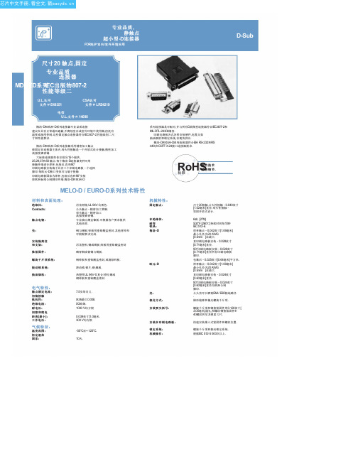
MD / ED系列
0.135 [3.43] 0.352 [8.94]
对于焊杯触点 ,指定 在步骤 4代码 2
订购信息.
典型型号: ED15M200T2Z
修正公头性和母头性提供偏光螺旋千斤顶. 指定订购信息步骤 7码 T6.
典型型号: MD15M200T6Z
直印刷电路板安装连接器
CODE NUMBER
HDC
6 0.375 [9.53] 0.360 [9.14]
指定订购信息步骤 6代码 F或 Q. F代表铁 素体电感和 Q为铁素体电感与推入式紧固件 .
L 90°印 刷 电 路 板 安 装 连 接 器
铁素体电感酒吧
A
0.135±0.005 [3.43±0.13]
Fixed female jackscrews
六标准连接器变体安排,9,15个提供, 25,29,37和50 触点.每个梅洛-D连接器变种可用 接触终端进行焊杯,包装后,直和90°
印刷电路板安装端子具有三个印刷电路板一个选择
脚印.每欧元-D接口变体可与端子接触 印刷电路板国家为焊杯,包装后直和90°安装 按欧洲标准公制脚印终端.梅洛-D和欧洲-D
钢与锡板;锌板用重铬酸盐密封.其他材料和 可根据要求完成.
尼龙塑料,铜或锡板;锌板用重铬酸盐密封 . 磷青铜或铍铜与锡板.
钢锌板和重铬酸盐密封,或清除锌板.
滑动锁,锁片,钢,镍板.
热塑性UL 94V-0.复合材料,铜或 钢锌板和重铬酸盐密封.
机械特性:
固定触点:
在绝缘体: 耐焊 铁热:
梅洛 -D
欧元 -D
可选壳件
与环球 FLOAT支架 [F]
0.120±0.010 [3.05±0.25]
TMF3202Z中文资料
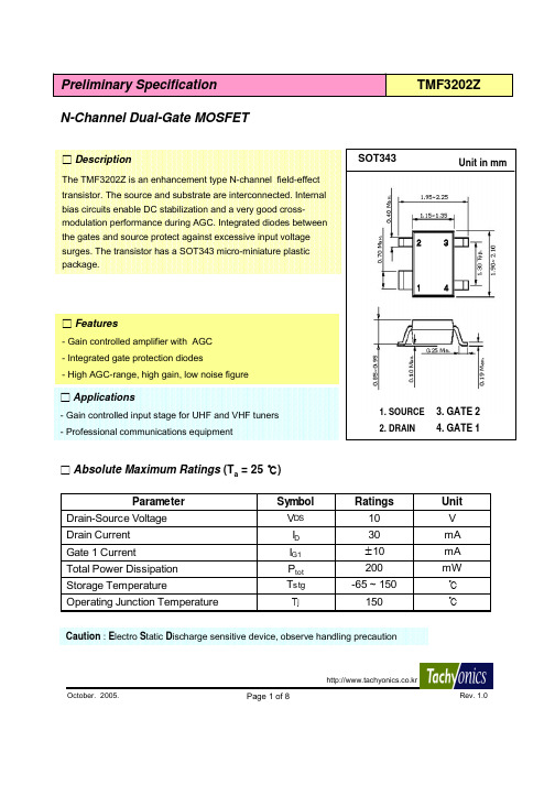
元器件交易网Preliminary Specification N-Channel Dual-Gate MOSFET□ DescriptionThe TMF3202Z is an enhancement type N-channel field-effect transistor. The source and substrate are interconnected. Internal bias circuits enable DC stabilization and a very good crossmodulation performance during AGC. Integrated diodes between the gates and source protect against excessive input voltage surges. The transistor has a SOT343 micro-miniature plastic package.TMF3202ZSOT343Unit in mm2314□ Features- Gain controlled amplifier with AGC - Integrated gate protection diodes - High AGC-range, high gain, low noise figure□ Applications- Gain controlled input stage for UHF and VHF tuners - Professional communications equipment1. SOURCE 2. DRAIN3. GATE 2 4. GATE 1□ Absolute Maximum Ratings (Ta = 25 ℃)Parameter Drain-Source Voltage Drain Current Gate 1 Current Total Power Dissipation Storage Temperature Operating Junction Temperature Symbol VDS ID IG1 Ptot Tstg Tj Ratings 10 30 ±10 200 -65 ~ 150 150 Unit V mA mA mW ℃ ℃Caution : Electro Static Discharge sensitive device, observe handling precautionhttp://www.tachyonics.co.kr October. 2005.Page 1 of 8Rev. 1.0元器件交易网Preliminary Specification□ DC Characteristics( Tj = 25 ℃, unless otherwise specified )PARAMETER Drain-source breakdown voltage Gate1-source breakdown voltage Gate2-source breakdown voltage Forward source-gate1 voltage Forward source-gate2 voltage Gate1-source threshold voltage Gate2-source threshold voltage Drain-source current Gate1 cut-off current Gate2 cut-off current SYMBOL V(BR)DSS V(BR)G1-SS V(BR)G2-SS V(F)S-G1 V(F)S-G2 VG1-S(th) VG2-S(th) IDSX IG1-S IG2-S CONDITION VG1-S=VG2-S=0; ID=10㎂ VG2-S=VDS=0; IG1-S=10㎃ VG1-S=VDS=0; IG2-S=10㎃ VG2-S=VDS=0; IS-G1=10㎃ VG1-S=VDS=0; IS-G2=10㎃ VDS=5V; VG2-S=4V; ID=100㎂ VDS=5V; VG1-S=4V; ID=100㎂ VG2-S=4V; VDS=5V; RG=62㏀ VG1-S=5V; VG2-S=VDS=0 VG2-S=5V; VG1-S=VDS=0 MIN. 10 6 6 0.5 0.5 0.3 0.3 8 -TMF3202ZMAX. 10 10 1.5 1.5 1.0 1.2 16 10 10UNIT V V V V V V V ㎃ ㎁ ㎁□ AC Characteristics( Common source; Ta = 25 ℃, VG2-S = 4V, VDS =5V, ID =12mA ;unless otherwise specified )PARAMETER Forward transfer admittance Input capacitance at gate1 Input capacitance at gate2 Output capacitance Reverse transfer capacitance SYMBOL IyFSI Cig1-ss Cig2-ss Coss Crss CONDITIONS MIN. TYP. MAX. UNITTj=25℃ f=1MHz f=1MHz f=1MHz f=1MHz f=200MHz; Zi = S11 , Zo = S22* *25 30 27 24 9030 1.7 3.3 0.9 15 33 30 27 1.2 1.5 -40 2.2 25 2.0 -mS ㎊ ㎊ ㎊ fF ㏈ ㏈ ㏈ ㏈ ㏈ ㏈㎶Power gainGtrf=400MHz; Zi = S11*, Zo = S22* f=800MHz; Zi = S11*, Zo = S22* f=400MHz; Zi = S11 opt(NF)Noise figureNFf=800MHz; Zi = S11 opt(NF) k=1%, fw=50MHz; funw=60MHz AGC = 0dBCross-modulation Xmodk=1%, fw=50MHz; funw=60MHz AGC = 10dB k=1%, fw=50MHz; funw=60MHz AGC = 40dB-92-㏈㎶100105-㏈㎶http://www.tachyonics.co.kr October. 2005.Page 2 of 8Rev. 1.0元器件交易网Preliminary Specification□ Equivalent circuit (Top view) 3 4 □ Making 3TMF3202Z42 tachyonics X1 1 3 4 2 2 3 42 tachyonics X2 1DB12 1 11 Diode DIODE21 Diode DIODE12□ Pin ConfigurationPIN 1 2 3 DESCRIPTION SOURCE DRAIN GATE2 GATE1□ Test circuitV_DC VAGC 1 1 R RAGC R=10 kOhm 2 2 2 14C CAGC C=4.7 nF 1 C CD C=4.7 nF 1 2 2 R RL R=50 Ohm 1 1 2 1 1 C CDB C=4.7 nF 1C CIN C=4.7 nF 1 R RSOURCE R=50 Ohm 2 1 V_AC SRC1 1 2 1 2 1 R RIN R=50 Ohm R RGB R=68 kOhm tachyonics X2 1 V_DC VGB 1 2 1 Diode DIODE1 1 1 1 2 1 2 3 4 2 2 3 42 tachyonics X1 12 L LD L=2.2 uH2 1Diode DIODE22 1V_DC VDBFig1. Test Cross-modulation test set-uphttp://www.tachyonics.co.kr October. 2005.Page 3 of 8Rev. 1.0Scattering parameters元器件交易网Preliminary Specification□ GraphsTMF3202ZID [ m A ]45 40 35 30 25 20 15 10 5 0 0.00 0.50 1.00 1.50 2.002V VG2=4V 3.5V 3V 2.5VID [ m A ]30 25 20 15 10 V G1-S : 1.5V1.4V 1.3V 1.2V 1.1V 1V 0.9V1.5V51V02.50 VG1-S [V]0123456 V DS [V ]7VDS =5V, Tj = 25 ℃ Fig.2 Transfer characteristics300 IG 1 [ u A ]VG2=4V 3.5V 3VVG2-S = 4V, Tj = 25 ℃ Fig3. Output characteristics| y fs| [m S ]25040 35 30 254V 3.5V 3V2002.5V1502V20 152.5V1001.5V10 5 0501VVG2-S = 2V0 4 8 12 16 20 ID [mA]0 0.000.501.001.502.00 VG1-S [V]2.50VDS =5V, Tj = 25 ℃ Fig.4 Gate1 Current as a function of gate1 VoltageVDS =5V, Tj = 25 ℃ Fig5. Forward transfer admittance as a function of drain currenthttp://www.tachyonics.co.krOctober. 2005.Page 4 of 8Rev. 1.0元器件交易网Preliminary SpecificationTMF3202Z□ GraphsID [ m A ]ID [ m A ]2016 14 12 10 8161286 4 240 0 20 40 60 80 100 IG1 [uA]0 0 0.5 1 1.5 2 2.5 3 3.5 4 4.5 5 VGG [V]VDS= 5V, V G2-S = 4V, Tj = 25 ℃ Fig6. Drain current as a function of gate1 currentVDS= 5V, V G2-S = 4V, RGB=62㏀, Tj = 25 ℃ Fig7. Drain current as a function of gate1 supply voltage18 16 14 12 10 8 6 4 2 0 0 1 2 3 4R G1 = 33KΩ 39KΩ 51KΩID [ m A ]ID [ m A ]2014 12 10VGG = 5V 4.5V 4V 3.5V 3V62KΩ75KΩ 92KΩ 100KΩ8 6 4 2 05 6 VGG=VDS [V]0123456 VG2-S [V]V G2-S = 4V, Tj = 25 ℃, RGB= (Connected to VGG) Fig8. Drain current as a function of gate1 and drain supply voltage ; see Fig1VDS= 5V, Tj = 25 ℃, RGB=62㏀ Fig9. Drain current as a function of gate2 voltagehttp://www.tachyonics.co.kr October. 2005.Page 5 of 8Rev. 1.0元器件交易网Preliminary Specification□ GraphsTMF3202ZIG 1 [ u A ]70 60 50 40 30 20 10 0 0.003.5V 3V VGG : 5V 4.5V 4V0 G a in r e d u c t io n [ d B ]-10-20-30-40-501.002.003.004.005.006.00 VG2-S [V]01234 VAGC [V]VDS= 5V, RGB= 62㏀, Tj = 25 ℃ ;Connected to VGB Fig10. Gate1 current as a function of gate2 voltagef=50MHz, Pin=-30dBm, VDS= 5V, VGB= 5V, RGB=62㏀ Tj = 25 ℃ Fig11. Typical Gain reduction as a function of AGC Voltage ; see Fig1ID [ m A ]14 12 10 8 6 4 2 0 0 10 20 30 40 50 gain reduction [dB]f=50MHz, Pin=-30dBm, VDS= 5V, VGB= 5V, RGB=62㏀ Fig12. Drain current as a function of gain reduction ; see Fig1http://www.tachyonics.co.kr October. 2005.Page 6 of 8Rev. 1.0元器件交易网Preliminary SpecificationTMF3202Z□ GraphsY iS [ m S]| yrs | [ u S ]10010φrs100 100 -100bis110-10 10|yrs|gis0 10 100 1000 f [MHz]1 10 100-1 1 1000f [MHz]VDS= 5V, V G2-S = 4V Fig13. Input admittance as a function of frequencyVDS= 5V, V G2-S = 4V Fig14. Reverse transfer admittance and phase as a function of frequency| yfs | [ m S ]|yfs|φfs [ d eg ]100-100 10010.00bos1.00 Y o S [ m S]10-10 10φfs0.10gos1 10 100-1 1 10000.01 10 100 1000 f [MHz]f [MHz]VDS= 5V, V G2-S = 4V Fig15. Forward transfer admittance and phase as a function of frequencyVDS= 5V, V G2-S = 4V Fig16. Output admittance as a function of frequencyhttp://www.tachyonics.co.krOctorber. 2005.Page 7 of 8Rev. 1.0φ rs [ d e g ]1000-1000 1000元器件交易网Preliminary Specification□ Scattering parameters(VG2-S = 4V, VDS =5V, ID =12mA, Ta = 25 ℃)Input Reflection CoefficientTMF3202ZReverse Transmission, dB 0-20 dB(S(1,2))freq (10.00MHz to 1.000GHz)S(1,1)-40-60-80 1E71E8 freq, HzOutput Reflection Coefficient1E9Forward Transmission, dB 12 10 8 dB(S(2,1)) 6 4 2 0 1E7S(2,2)1E8 freq, Hz1E9freq (10.00MHz to 1.000GHz)VDS=5V, VG2-S=4V, ID=12mA f (MHz) 50 100 200 300 400 500 600 700 800 S11 Magnitude (ratio)0.897 0.915 0.952 0.938 0.912 0.836 0.863 0.830 0.800S21 Angle (deg)0.974 -5.323 -17.920 -27.300 -35.160 -43.000 -50.800 -57.600 -63.470S12 Angle (deg)171.7 165.5 153.1 141.5 130.8 120.1 110.1 98.8 87.8S22 Angle (deg)93.0 91.7 89 89.2 92.6 95.6 100.4 104.6 110.7Magnitude (ratio)3.93 3.81 3.58 3.40 3.20 3.04 2.89 2.75 2.62Magnitude (ratio)0.001 0.001 0.002 0.002 0.003 0.004 0.004 0.004 0.004Magnitude (ratio)1.006 0.998 0.982 0.968 0.966 0.964 0.968 0.968 0.973Angle (deg)-1.86 -4.89 -10.97 -16.13 -20.8 -26.01 -30.59 -35.8 -40.87http://www.tachyonics.co.kr Octorber. 2005.Page 8 of 8Rev. 1.0。
维智WSDA系列伺服驱动器用户手册(EtherCAT总线通信型)-R4
维智WSDA系列伺服驱动器用户手册(EtherCAT总线通信型)版次:2020年10月12日第4版作者:产品应用测试部上海维宏电子科技股份有限公司目录1 安全注意事项 (1)1.1 警告 (1)1.2 注意 (2)2 基本信息 (3)2.1 前面板结构 (3)2.2 铭牌 (4)2.3 控制模式 (5)2.4 规格与功能 (5)2.4.1 基本规格 (5)2.4.2 从站规格 (7)2.4.3 基本功能 (8)2.4.4 保护功能 (8)2.5 产品安装 (8)2.6 系统接线图 (10)3 配线 (13)3.1 主回路接线 (13)3.1.1 端子 (13)3.1.2 电线规格 (14)3.1.3 接线说明 (17)3.2 USB通讯接口CN1接线 (18)3.2.1 端口定义 (18)3.2.2 线缆 (19)3.3 总线接口 CN2A/B 接线 (20)3.3.1 接线图 (20)3.3.2 线缆 (20)3.4 电机编码器线接口CN4接线 (21)3.4.1 端口定义 (21)3.4.2 说明 (22)3.4.3 线缆 (23)3.5 外置再生制动电阻器连接 (24)4 驱动器面板 (29)4.1 概述 (29)4.2 监视器模式 (31)4.3 参数设定模式 (41)4.4 EEPROM 写入模式 (41)4.5 辅助功能模式 (42)4.5.1 概述 (42)4.5.2 设置站别名 (44)4.5.3 解除报警 (44)4.5.4 试运行电机 (45)4.5.5 清零绝对值编码器 (45)4.5.6 初始化参数 (46)4.5.7 解除前面板锁定 (46)4.5.8 注册驱动器 (46)4.5.9 初始化对象字典 (47)4.6 驱动器面板锁定 (48)5 电机试运行 (48)5.1 准备工作 (48)5.2 进行基本设定 (48)5.2.1 打开伺服 (49)5.2.2 选择电机旋转方向 (49)5.2.3 启用超程防止功能 (49)5.2.4 设定电机过载率 (50)5.2.5 启用制动器 (50)5.2.6 伺服断开及报警时停止电机 (50)5.3.1 使用 iMotion 软件 (51)5.3.2 使用驱动器面板 (51)5.4 故障排查 (51)6 控制系统连接 (54)6.1 选择系统类型 (54)6.2 设置关联参数 (54)6.2.1 设置控制系统参数 (54)6.2.2 设置维智伺服驱动器参数 (55)6.3 设置站别名 (55)6.4 设定基准或回机械原点 (55)6.4.1 设定基准 (55)6.4.2 回机械原点 (56)6.5 运行电机 (56)7 绝对式系统 (56)7.1 安装与更换电池 (56)7.2 自制绝对式编码器电缆 (58)7.3 启用绝对值功能 (58)7.4 启用无限旋转绝对式功能 (58)8 增益调整 (58)8.1 准备工作 (58)8.1.1 设定驱动禁止输入 (59)8.1.2 设定转矩限制 (59)8.1.3 设定过速度保护 (59)8.1.4 设定位置偏差过大保护 (59)8.1.5 设定电机可动范围 (60)8.2 推定惯量比 (60)8.3 设置自适应滤波器 (61)8.3.1 操作步骤 (62)8.3.2 故障排查 (62)8.3.3 相关信息 (63)8.4 自动调整增益 (63)8.4.1 操作步骤 (64)8.4.3 相关信息 (65)8.5 手动调整增益 (67)8.5.1 执行基本调整 (68)8.5.2 切换增益 (69)8.5.3 抑制机械共振 (75)8.5.4 设置 2 段转矩滤波器 (76)8.6 总线控制系统调整增益 (77)9 驱动器注册 (77)9.1 获取序列号 (77)9.1.1 通过 iMotion 软件 (78)9.1.2 通过驱动器面板 (79)9.2 获取注册码 (80)9.3 注册驱动器 (81)10 异常与对策 (82)10.1 异常时应对思路 (82)10.2 警告 (83)10.2.1 查找警告 (83)10.2.2 警告码 (83)10.3 SDO传输中止码 (84)10.4 错误码一览表 (85)10.5 错误码详情 (90)10.5.1 Err10系列 (90)10.5.2 Err20系列 (97)10.5.3 Err30系列 (101)10.5.4 Err40系列 (105)10.5.5 Err50系列 (108)10.5.6 Err70系列 (112)10.5.7 Err80系列 (115)10.5.8 Err90系列 (124)10.5.9 其他错误码 (125)10.5.10 解除错误 (125)11 参数 (126)11.2 [分类 0]基本设定 (126)11.2.1 Pr001 (126)11.2.2 Pr002 (127)11.2.3 Pr003 (127)11.2.4 Pr004 (128)11.2.5 Pr011 (128)11.2.6 Pr012 (129)11.2.7 Pr013 (130)11.2.8 Pr014 (131)11.2.9 Pr015 (131)11.2.10 Pr016 (132)11.2.11 Pr017 (132)11.2.12 Pr018~Pr019 (133)11.2.13 Pr024 (134)11.3 [分类 1]增益调整 (134)11.3.1 Pr100~Pr104 (134)11.3.2 Pr105~Pr109 (136)11.3.3 Pr110 (137)11.3.4 Pr111 (138)11.3.5 Pr112 (138)11.3.6 Pr113 (138)11.3.7 Pr114 (139)11.3.8 Pr115 (140)11.3.9 Pr116 (142)11.3.10 Pr117 (142)11.3.11 Pr118 (142)11.3.12 Pr119 (143)11.3.13 Pr120 (143)11.3.14 Pr121 (144)11.3.15 Pr122 (144)11.3.16 Pr123 (144)11.3.17 Pr124 (145)11.3.19 Pr126 (145)11.3.20 Pr127 (146)11.4 [分类 2]控制抑制功能 (146)11.4.1 Pr200 (146)11.4.2 Pr201~Pr203 (146)11.4.3 Pr204~Pr206 (147)11.4.4 Pr207~Pr209 (149)11.4.5 Pr210~Pr212 (150)11.4.6 Pr214~Pr215 (151)11.4.7 Pr216~Pr217 (151)11.4.8 Pr218~Pr219 (152)11.4.9 Pr220~Pr221 (152)11.4.10 Pr222 (153)11.4.11 Pr223 (154)11.5 [分类 3]速度/转矩控制 (155)11.5.1 Pr300 (155)11.5.2 Pr302 (156)11.5.3 Pr304 (156)11.5.4 Pr312~Pr313 (157)11.5.5 Pr314 (158)11.5.6 Pr317、Pr318、Pr321、Pr322 (158)11.5.7 Pr323 (160)11.5.8 Pr326 (160)11.5.9 Pr327 (161)11.5.10 Pr343 (161)11.5.11 Pr344 (161)11.5.12 Pr345 (162)11.5.13 Pr346 (162)11.6 [分类 4] I / F 监视器设定 (162)11.6.1 Pr400~Pr406 (162)11.6.2 Pr408~Pr411 (165)11.6.3 Pr430 (167)11.6.5 Pr432 (168)11.6.6 Pr433 (168)11.6.7 Pr434 (169)11.6.8 Pr435 (169)11.6.9 Pr436 (170)11.6.10 Pr437 (171)11.6.11 Pr438 (171)11.6.12 Pr439~Pr440 (172)11.6.13 Pr441 (173)11.6.14 Pr449 (173)11.6.15 Pr450 (174)11.7 [分类 5]扩展设定 (174)11.7.1 Pr503 (174)11.7.2 Pr504 (174)11.7.3 Pr505 (175)11.7.4 Pr506 (176)11.7.5 Pr507 (177)11.7.6 Pr508 (177)11.7.7 Pr509 (177)11.7.8 Pr510 (178)11.7.9 Pr511 (179)11.7.10 Pr512 (179)11.7.11 Pr513 (179)11.7.12 Pr514 (180)11.7.13 Pr516 (180)11.7.14 Pr520 (180)11.7.15 Pr521 (181)11.7.16 Pr522 (181)11.7.17 Pr523 (181)11.7.18 Pr524 (181)11.7.19 Pr525 (182)11.7.20 Pr526 (182)11.7.22 Pr533 (184)11.7.23 Pr535 (184)11.7.24 Pr540 (184)11.7.25 Pr541 (185)11.8 [分类 6]特殊设定 (185)11.8.1 Pr601 (185)11.8.2 Pr602 (185)11.8.3 Pr604 (185)11.8.4 Pr607 (186)11.8.5 Pr608 (186)11.8.6 Pr609 (186)11.8.7 Pr611 (187)11.8.8 Pr612 (187)11.8.9 Pr615 (187)11.8.10 Pr617 (188)11.8.11 Pr623 (188)11.8.12 Pr624 (189)11.8.13 Pr627 (189)11.8.14 Pr628 (189)11.8.15 Pr629 (189)11.8.16 Pr630 (190)11.8.17 Pr632 (190)11.8.18 Pr633 (192)11.8.19 Pr638 (192)11.8.20 Pr640 (193)11.8.21 Pr642 (193)11.8.22 Pr643 (194)11.8.23 Pr647 (194)11.8.24 Pr650 (194)11.8.25 Pr651 (195)11.8.26 Pr660 (195)12 EtherCat通信规格 (195)12.2 帧结构 (196)12.3 ESC地址空间 (197)12.4 通信状态 (197)12.5 SDO (198)12.6 PDO (198)12.6.1 PDO映射 (199)12.6.2 分配对象 (200)12.6.3 映射配置 (200)12.7 DC通信同步模式 (201)12.8 SII EEPROM (201)12.9 寻址模式 (201)13 对象字典 (202)13.1 概述 (202)13.1.1 分类 (202)13.1.2 数据类型 (203)13.1.3 相关用语 (203)13.2 通信对象 (204)13.2.1 设备信息 (204)13.2.2 同步管理器通讯类型 (208)13.2.3 PDO通讯 (210)13.2.4 同步管理器 2 和 3 同步对象 (240)13.2.5 对象写入 EEPROM (250)13.2.6 对象恢复出厂 (251)13.2.7 故障履历 (252)13.3 驱动器参数对象 (259)13.3.1 2100h (259)13.3.2 2101h (260)13.3.3 2102h (262)13.3.4 2103h (263)13.3.5 2200h (264)13.4 厂商定义对象 (265)13.5 辅助功能对象 (266)13.5.1 信息监视器对象 (266)13.5.2 多圈绝对式编码器清零 (277)13.6 驱动协议对象 (277)13.6.1 功率驱动系统状态机 (277)13.6.2 控制模式设置 (283)13.6.3 位置控制模式 (287)13.6.4 速度控制模式 (325)13.6.5 转矩控制模式 (335)13.6.6 模式共通功能 (343)14 对象字典一览表 (370)14.1 1000h~1FFFh (370)14.2 2000h~2FFFh (378)14.3 3000h~30FFh (379)14.4 3100h~37FFh (392)14.5 6000h~6FFFh (394)1安全注意事项注意事项根据不遵守可能会造成危害的程度,分为警告和注意类型:警告:特别需要提示的内容,如果不遵守此类信息,可能会造成人身伤害甚至是死亡、机器损坏、或者其他财产损失。
ZSR850C中文资料(Zetex Semiconductors)中文数据手册「EasyDatasheet - 矽搜」

2.85至 12伏 固 定 正
当地电压稳压器
设备描述 该ZSR系列三端固定正电压
稳压器内部电路电流限制和 热关断使得设备难以
破坏.该电路设计允许创建任何 定制电压范围为2.85至12伏.该
器件采用小外形表面贴装
封装,非常适合应用中节省空间 重要,以及贯通孔TO92样式 包装.该器件适合当地电压 调节应用中,问题可能是 分布式单一来源调控遭遇, 以及moregeneralvoltagereg ulation 应用.
该ZSR系列节目性能优于其他地方稳压器.初始 输出电压防护持为在2.5%与通常350μA静态电流.输出 电压变化,与输入电压和负载电流,比同类设备低 得多.该ZSR器件无需外部元件完全稳定.
ZSR
系列
特征 小外形SO8和SOT223封装 TO92封装 2.85〜12电压 输出电流高达200mA
紧初始容差 低静态电流
14
13.7
0.25
V mV/°C
第 3期 - 2001年 9月 5
25℃,必须进行线性降额至零 Tamb =125°C. 2. 以下数据表示脉冲测试条件下与结温在试验开始指 示.中,规定条件装置连续操作可能会超 过所选择包功率耗散限制.
功耗(T SOT223 TO92
S08
amb =25°C) 2W(Note 3) 600mW
780mW(Note 3)
3. 最大功耗,为SOT223和 SO8封装,来计算假定该设备被安装在PCB 2英寸见方 . 4. 该装置关闭功能,如果它温度超过其设计极限作为 在外部故障,短路等.如果调节器从感应源再大电 压瞬变供给,对调节器输入,能导致如若可能发生 操作关闭电路工作.据表示一个电容器(1μF以上)应
大连东福彩色液晶显示器模块使用说明书

EDM12232-06图形点阵式液晶显示模块使用说明大连东福彩色液晶显示器有限公司1. 使用范围----------------------------------------------------22. 质量保证----------------------------------------------------23. 性能特点----------------------------------------------------24. 外形图-------------------------------------------------------65. I/O接口特性-----------------------------------------------76. 质量等级---------------------------------------------------167. 可靠性---------------------------------------------------198. 生产注意事项---------------------------------------------199. 使用注意事项---------------------------------------------20第 2 页共 20页第 3 页 共 20页1、使用范围该检验标准适用于大连东福公司设计提供的标准液晶显示模块。
如果在使用中出现了异常问题或没有列明的项目,建议同最近的供应商或本公司联系。
2、质量保证 如在此手册列明的正常条件下使用、储存该产品,公司将提供12个月的质量保证。
3、性能特点3-1.性能:显示方式 : 半透、正显黄绿色 STN LCD 显示颜色 : 显示点: 深蓝色背景:黄绿色显示形式 : 122(w)×32 (h) 全点阵 输入数据 : 来自MPU 的8位并行数据接口 驱动路数 : 1/32 Duty视 角 :6 点3-2.机械性能:项 目 规 格 单位外形尺寸 84.0(W)×44.0(H) ×14.0 Max. Mm 显示点阵数 122(W) ×32 (H) Dots —视 域 60.0(W)×18.0(H) Mm 显示图形域 48.76(W)×15.32H) Mm 点间距 0.4(W)×0.45(H) Mm 点尺寸 0.36(W)×0.41(H) Mm 重量 Approx. 40 G3-3. 极限参数:项目 符 号 最小值 最大值 单位 注 释逻辑 Vdd-0.3 7.0 V 电源电压 LCD 驱动 Vdd – Vee VDD-13.5VDD-3.5V 输入电压 Vi -0.3 VDD+0.3V 操作温度 Top -10 50 ℃ 储存温度 Tstg -20 60 ℃ 湿度 — — 90 %RH 背光驱动动电压 VBL — 5.0 VLCD 模块使用手册第 4 页 共 20页3-4. 电气特性:3-4-1 电气参数项 目 符 号 条 件 最小值典型值 最大值 单 位 逻辑 Vdd 4.5 5.00 5.5电源电压LCD 驱动 Vdd–Vee — 5.0 —高电平 Vih Vdd=5V ±5% 2.0 — Vdd输入电压低电平 Vil 0 — 0.8V频 率 Fflm Vdd=5V — 75 — Hz逻辑 Idd — 0.44 —功 耗 LCD 驱动 Iee Vdd=5V Vdd–Vee=5.2VFflm=75Hz — 0.42 —mA Ta= -20℃φ=0°,θ=0°— — —Ta= 25℃φ=0°,θ=0°— 5.0 — LCD 驱动电压 (推荐电压) Vdd–Vee Ta= 60℃φ=0°,θ=0° — — —VNote: <1> 驱动路数=1/32 <2> 所有点在静态条 3-5. 光电特性项 目 符号温度 条件 最小值典型值最大值 单位 注释 -20℃ — — —25℃ — 5.0 — LCD 驱动电压 (推荐电压) V LCD 60℃ φ=0°,θ=0°— — — V 1,2,5-20℃ — 750 1100 上升时间 tr25℃ — 150 200 -20℃ — 1000 1500响应时间 衰退时间 td 25℃ φ=0°,θ=0° — 150 200Ms 1,3,5垂直 — +50/-45—视 角Δφ 25℃水平 — +55/-55—deg. 1,4,5对比度 K 25℃ φ=0°,θ=0°2 — 5 — 1,5,6注意:<1> φ和θ的定义<2> 在此电压范围内能获得对比度大于2(k≥2)第 5 页共 20页第 6 页 共 20页注意:<6> 对比度定义(K)正显负显非选择点的亮度(B2) 选择点的亮度(B1)4、外形图第 7 页 共 20页5、I/O 接口特性5-1. I/O 接口表:管脚号 符号功 能1 Vcc 电源电压2 Vss 接地3 Vee LCD 驱动电压4 RES 复位信号5 E1 使能信号6 E2 使能信号7 R/W 读写控制信号8 A0 显示数据.指令数据控制信号 9~16 DB0~DB7数据线 17 LED+ 背光电源 18 LED - 背光电源5-2.时序及时序图:项目 符号 条件最小值 最大值 单位 E 使能信号周期 Tc 1000 — E 高电屏保持时间 Twh 450 — E 低电屏保持时间 Twl450 — E 上升时间 Tr — 25 E 下降时间 Tf — 25R/W 建立时间 Tasu140 —R/W 保持时间 Tah10 — 数据上升时间 Tdsu 200 — 数据延时时间 Td — 320 写数据保持时间 Tdhw 20 — 读数据保持时间 TdhrVdd=5V ±5%Vss=0V Ta=25℃ 10 —ns时序图如下:(a) 写时序图第 8 页 共 20页(b)读时序图5-3. 电源连接图5-4. 电路图解(图解参见Fig.5-4)LCD 模块需逻辑电压(Vdd )和LCD 驱动电压(Vee )注释: 当信号线直接连到C-MOS电路且没有内部上拉或下拉电阻时,有必要隔离外部干扰来保护信号线。
EMIFYY-xxxzzF4中文资料
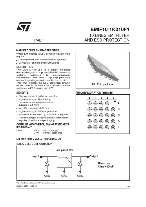
1/6August 2003 - Ed: 4AIEC61000-4-2Level 415kV (air discharge)8kV (contact discharge)MIL STD 883E -Method 3015-6Class 3COMPLIES WITH THE FOLLOWING STANDARDS:s EMI symmetrical (I/O)low-pass filter s High efficiency in EMI filtering s Very low PCB space consuming:2.57mm x 2.57mms Very thin package:0.65mms High efficiency in ESD suppressions High reliability offered by monolithic integration sHigh reducing of parasitic elements through in-tegration &wafer level packaging.BENEFITS10 LINES EMI FILTER AND ESD PROTECTIONIPAD TMWhere EMI filtering in ESD sensitive equipment is required :s Mobile phones and communication systems sComputers,printers and MCU BoardsMAIN PRODUCT CHARACTERISTICS:The EMIF10-1K010F1is a highly integrated devices designed to suppress EMI/RFI noise in all systems subjected to electromagnetic interferences.The EMIF10flip chip packaging means the package size is equal to the die size.This filter includes an ESD protection circuitry which prevents the device from destruction when subjected to ESD surges up 15kV.DESCRIPTIONTM :IPAD is a trademark of STMicroelectronics.EMIF10-1K010F12/6Fig.1:S21(dB)attenuation measurement and Aplac simulation.1101001,000-100-80-60-40-200frequency (MHz)Fig.2:Analog crosstalk measurements.Symbol Parameter and test conditionsValue Unit T j Junction temperature 125°C T op Operating temperature range -40to +85°C T stgStorage temperature range-55to +150°CABSOLUTE MAXIMUM RATINGS (T amb =25°C)Symbol ParametersV BR Breakdown voltage I RM Leakage current @V RM V RM Stand-off voltage V CL Clamping voltage R d Dynamic impedance I PP Peak pulse currentR I/O Series resistance between Input &OutputC lineInput capacitance per lineELECTRICAL CHARACTERISTICS (T amb = 25°C)Symbol Test conditionsMin Typ Max Unit V BR I R =1mA6810V I RM V RM =3V per line500nA R I/O 90010001100ΩC lineAt 0V bias 80100120pFEMIF10-1K010F13/6V β21Fig.3:Digital crosstalk measurement.V(in1)V(out1)Fig.4:ESD response to IEC61000-4-2(+15kV air discharge)on one input V(in)and on one output V(in1)V(out1)Fig.5:ESD response to IEC61000-4-2(-15kV air discharge)on one input V(in)and on one output (Vout).100C(pF)F=1MHz Fig.6:Line capacitance versus applied voltage.EMIF10-1K010F14/6Fig.7:Aplac model single line structure.aplacvar Cz57pF aplacvar Rseries 960aplacvar cap_line 0.8pF aplacvar Ls0.6nH aplacvar Rbump 50m aplacvar Lbump 50pH aplacvar Rs0.15aplacvar Csubump 15pF aplacvar Rsubump 0.15aplacvar Rsub 0.1aplacvar lhole 1.2nH opt aplacvar Rhole 0.15aplacvar cap_hole 0.15pF aplacvar Rgnd 0.25aplacvarIgnd0.4nHModel demif10BV = 7IBV = 1m CJO = Cz M = 0.3333Rs = 1VJ = 0.6TT = 100nFig.8:Aplac model parameters.ORDER CODEEMIF10-1K010F15/6PACKAGE MECHANICAL DATA FLIP CHIPMARKINGFOOT PRINT RECOMMENDATIONSEMIF10-1K010F16/6Information furnished is believed to be accurate and reliable.However,STMicroelectronics assumes no responsibility for the consequences of use of such information nor for any infringement of patents or other rights of third parties which may result from its use.No license is granted by implication or otherwise under any patent or patent rights of STMicroelectronics.Specifications mentioned in this publication are subject to change without notice.This publication supersedes and replaces all information previously supplied.STMicroelectronics products are not au-thorized for use as critical components in life support devices or systems without express written approval of STMicroelectronics.The ST logo is a registered trademark of STMicroelectronics.All other names are the property of their respective owners.©2003STMicroelectronics -All rights reserved.STMicroelectronics GROUP OF COMPANIESAustralia -Belgium -Brazil -Canada -China -Czech Republic -Finland -France -Germany -Hong Kong -India -Israel -Italy -Japan -Malaysia -Malta -Morocco -Singapore -Spain -Sweden -Switzerland -United Kingdom -United StatesPACKINGOrdering code Marking Package Weight Base qty Delivery mode EMIF10-1K010F1FDTFlip Chip9.2mg5000Tape &reel (7”)OTHER INFORMATION Note:More information are available in the application notes:-AN1235:''Flip-Chip:Package description and recommandations for use''-AN1751:"EMI Filters:Recommendations and measurements"。
电子元器件zx3cd1s1m832中文资料_数据手册_IC数据表
SUMMARY PNP Transistor V CEO =-12V;R SAT = 65m ;C = -4A Schottky Diode V R = 40V; V F = 500mV (@1A); I C =1ADESCRIPTIONPackaged in the new innovative 3mm x 2mm MLP this combination dual comprises an ultra low saturation PNP transistor and a 1A Schottky barrier diode.This excellent combination provides users with highly efficient performance in applications including DC-DC and charging ers will also gain several other key benefits :Performance capability equivalent to much larger packages Improved circuit efficiency & power levelsPCB area and device placement savingsLower package height (0.9mm nom)Reduced component countFEATURES•Extremely Low Saturation Voltage (-140mV @1A)•H FE characterised up to -10A•I C = -4A Continuous Collector Current•Extremely Low V F , fast switching Schottky•3mm x 2mm MLPAPPLICATIONS•DC - DC Converters •Mobile Phones•Charging Circuits •Motor controlDEVICE MARKING1S1ZX3CD1S1M832ISSUE 1 - JUNE 2002MPPS™ Miniature Package Power Solutions12V PNP LOW SATURATION TRANSISTOR AND 40V, 1A SCHOTTKY DIODE COMBINATION DUAL1DEVICEREEL TAPE WIDTH QUANTITY PER REELZX3CD1S1M832TA 78mm 3000ZX3CD1S1M832TC138mm10000ORDERING INFORMATION3mm x 2mm Dual DieMLP3mm x 2mm Dual MLPunderside viewPINOUTh tt ps ://w ww .i ch un o mh t t p sn t.co mh tt ps ://w ww .i ch un t.co mh tt p s://w w w.h tt ps :co m.ic hu nt .c omh tt ps ://w ww .i ch un t.co mh tt p s://ww w.ih tt n t.c o m w .i ch un t.co mt tp s://ww w.ic hu nt .c omh tt ps ://w ww .i ch tt ://w w w .i c h u n t .cww .i ch un t.co mi ch un t.co mh tt ps ://w ww .i ch h t t p s ://ww ww .i ch un t.co mh tt ps ://w ww .i ch u/w ww .i ch un t.co mh tt ps ://w ww .i ch un //w ww .i ch un t.co mh tt ps ://w ww .i ch un t://w ww .i c h u n t.c o mw ww .i ch un t.s ://w w w .i cZX3CD1S1M832ISSUE 1 - JUNE 20022PARAMETERSYMBOL VALUE UNIT TransistorCollector-Base VoltageV CBO -20V Collector-Emitter Voltage V CEO -12V Emitter-Base Voltage V EBO -7.5V Peak Pulse CurrentI CM -12A Continuous Collector Current (a)(f)I C -4A Continuous Collector Current (b)(f)I C -4.4A Base CurrentI B 1000mA Power Dissipation at TA=25°C (a)(f)Linear Derating FactorP D 1.512W mW/°C Power Dissipation at TA=25°C (b)(f)Linear Derating FactorP D 2.4519.6W mW/°CPower Dissipation at TA=25°C (c)(f)Linear Derating FactorP D18W mW/°CPower Dissipation at TA=25°C (d)(f)Linear Derating FactorP D 1.139W mW/°CPower Dissipation at TA=25°C (d)(g)Linear Derating Factor P D1.713.6W mW/°CPower Dissipation at TA=25°C (e)(g)Linear Derating FactorP D324W mW/°CStorage Temperature RangeT stg-55to +150°C Junction TemperatureT j150°CABSOLUTE MAXIMUM RATINGS.PARAMETER SYMBOL VALUE UNIT Junction to Ambient (a)(f)R θJA 83°C/W Junction to Ambient (b)(f)R θJA 51°C/W Junction to Ambient (c)(f)R θJA 125°C/W Junction to Ambient (d)(f)R θJA 111°C/W Junction to Ambient (d)(g)R θJA 73.5°C/W Junction to Ambient (e)(g)R θJA41.7°C/WTHERMAL RESISTANCENotes(a) For a dual device surface mounted on 8 sq cm single sided 2oz copper on FR4 PCB, in still air conditions with all exposed pads attached . The copper area is split down the centre line into two separate areas with one half connected to each half of the dual device.(b) Measured at t<5 secs for a dual device surface mounted on 8 sq cm single sided 2oz copper on FR4 PCB, in still air conditions with all exposed pads attached.The copper area is split down the centre line into two separate areas with one half connected to each half of the dual device.(c) For a dual device surface mounted on 8 sq cm single sided 2oz copper on FR4 PCB, in still air conditions with minimal lead connections only.(d) For a dual device surface mounted on 10 sq cm single sided 1oz copper on FR4 PCB, in still air conditions with all exposed pads attached attached . The copper area is split down the centre line into two separate areas with one half connected to each half of the dual device.(e) For a dual device surface mounted on 85 sq cm single sided 2oz copper on FR4 PCB, in still air conditions with all exposed pads attached attached . The copper area is split down the centre line into two separate areas with one half connected to each half of the dual device.(f) For a dual device with one active die.(g) For dual device with 2 active die running at equal power.(h) Repetitive rating - pulse width limited by max junction temperature. Refer to Transient Thermal Impedance graph.(i) The minimum copper dimensions required for mounting are no smaller than the exposed metal pads on the base of the device as shown in the package dimensions data. The thermal resistance for a dual device mounted on 1.5mm thick FR4 board using minimum copper 1 oz weight, 1mm wide tracks and one half of the device active is Rth = 250°C/W giving a power rating of Ptot = 500mW.h tt ps ://w ww .i ch un t.co mh t t p sn t.co mh tt ps ://w ww .i ch un t.co mh tt p s ://ww w .h tt ps ://w ww .i ch un t.co m.ic hu nt .c omh tt ps ://w ww .i ch un t.co mh tt p s://ww w.ih tt ps ://w ww .i ch un t .c o m w .i ch un t.co mt tp s://ww w.ic hu nt .c omh tt ps ://w ww .i ch tt ps ://w w w .i c h un t .cww .i ch un t.co mi ch un t.co mh tt ps ://w ww .i ch h t t p s ://ww ww .i ch un t.co mh tt ps ://w ww .i ch u/w ww .i ch un t.co mh tt ps ://w ww .i ch un //w ww .i ch un t.co m h tt ps ://w ww .i ch un t://w ww .i ch u n t.c o m w ww .i ch un t.s ://w w w .i cZX3CD1S1M832ISSUE 1 - JUNE 20023TRANSISTOR TYPICAL CHARACTERISTICSh t t p sn t.co mh tt p s://w w w ..ic hu nt .c omh tt p s://ww w.io m w .i ch un t.co tt ps ://w ww .i cw w .i c h u n t .c ww .i ch un t.ct ps ://w ww .i ch h t t p s ://ww ww .i ch un t.ps ://w ww .i ch u/w ww .i ch un ts ://w ww .i ch un //w ww .i ch un ://w ww .i ch un t://w ww .i c h u n t.c o m w ww .i ch un t.s ://w w w .icZX3CD1S1M832ISSUE 1 - JUNE 20024PARAMETERSYMBOL VALUE UNIT Schottky DiodeContinuous Reverse VoltageV R 40V Forward Voltage @I F =1000mA(typ)V F 425A Forward CurrentI F 1850mA Average Peak Forward Current D=50%I FAV 3A Non Repetitive Forward Current t ≤100st ≤10ms I FSM 127A A Power Dissipation at TA=25°C (a)(f)Linear Derating FactorP D 1.212W mW/°C Power Dissipation at TA=25°C (b)(f)Linear Derating FactorP D 220W mW/°C Power Dissipation at TA=25°C (c)(f)Linear Derating FactorP D0.88W mW/°C Power Dissipation at TA=25°C (d)(f)Linear Derating FactorP D0.99W mW/°C Power Dissipation at TA=25°C (d)(g)Linear Derating FactorP D 1.3613.6W mW/°CPower Dissipation at TA=25°C (e)(g)Linear Derating Factor P D2.424W mW/°C Storage Temperature RangeT stg-55to +150°CJunction TemperatureT j125°CABSOLUTE MAXIMUM RATINGS.PARAMETER SYMBOL VALUE UNIT Junction to Ambient (a)(f)R θJA83°C/W Junction to Ambient (b)(f)R θJA 51°C/W Junction to Ambient (c)(f)R θJA 125°C/W Junction to Ambient (d)(f)R θJA 111°C/W Junction to Ambient (d)(g)R θJA 73.5°C/W Junction to Ambient (e)(g)R θJA41.7°C/WTHERMAL RESISTANCENotes(a) For a dual device surface mounted on 8 sq cm single sided 2oz copper on FR4 PCB, in still air conditions with all exposed pads attached . The copper area is split down the centre line into two separate areas with one half connected to each half of the dual device.(b) Measured at t<5 secs for a dual device surface mounted on 8 sq cm single sided 2oz copper on FR4 PCB, in still air conditions with all exposed pads attached.The copper area is split down the centre line into two separate areas with one half connected to each half of the dual device.(c) For a dual device surface mounted on 8 sq cm single sided 2oz copper on FR4 PCB, in still air conditions with minimal lead connections only.(d) For a dual device surface mounted on 10 sq cm single sided 1oz copper on FR4 PCB, in still air conditions with all exposed pads attached attached . The copper area is split down the centre line into two separate areas with one half connected to each half of the dual device.(e) For a dual device surface mounted on 85 sq cm single sided 2oz copper on FR4 PCB, in still air conditions with all exposed pads attached attached . The copper area is split down the centre line into two separate areas with one half connected to each half of the dual device.(f) For a dual device with one active die.(g) For dual device with 2 active die running at equal power.(h) Repetitive rating - pulse width limited by max junction temperature. Refer to Transient Thermal Impedance graph.(i) The minimum copper dimensions required for mounting are no smaller than the exposed metal pads on the base of the device as shown in the package dimensions data. The thermal resistance for a dual device mounted on 1.5mm thick FR4 board using minimum copper 1 oz weight, 1mm wide tracks and one half of the device active is Rth = 250°C/W giving a power rating of Ptot = 400mW.h tt ps ://w ww .i ch un t.co mh t t p sn t.co mh tt ps ://w ww .i ch un t.co mh tt p s ://ww w .h tt ps ://w ww .i ch un t.co m.ic hu nt .c omh tt ps ://w ww .i ch un t.co mh tt p s://ww w.ih tt ps ://w ww .i ch un t .c o m w .i ch un t.co mt tp s://ww w.ic hu nt .c omh tt ps ://w ww .i ch tt ps ://w w w .i c h un t .cww .i ch un t.co mi ch un t.co mh tt ps ://w ww .i ch h t t p s ://ww ww .i ch un t.co mh tt ps ://w ww .i ch u/w ww .i ch un t.co mh tt ps ://w ww .i ch un //w ww .i ch un t.co m h tt ps ://w ww .i ch un t://w ww .i c h u n t.c o m w ww .i ch un t.s ://w w w .i cZX3CD1S1M832ISSUE 1 - JUNE 20025SCHOTTKY TYPICAL CHARACTERISTICSh t t p sn t.co mh tt p s://w w w ..ic hu nt .c omh tt p s://ww w.io m w .i ch un t.co mt tp stt ps ://w ww .i cw w .i c h u n t .c ww .i ch un t.co mi ch ut ps ://w ww .i ch h t t p s ://ww ww .i ch un t.co mps ://w ww .i ch u/w ww .i ch un t.co ms ://w ww .i ch un //w ww .i ch un t.co m h ://w ww .i ch un t://w ww .i c h u n t.c o m w ww .i ch un t.s ://w w w .icZX3CD1S1M832ISSUE 1 - JUNE 20026PARAMETERSYMBOLMIN.TYP.MAX.UNITCONDITIONS.TRANSISTOR ELECTRICAL CHARACTERISTICS Collector-Base Breakdown VoltageV (BR)CBO -20-35V I C =-100A Collector-Emitter Breakdown VoltageV (BR)CEO -12-25V I C =-10mA*Emitter-Base Breakdown Voltage V (BR)EBO -7.5-8.5V I E =-100A Collector Cut-Off Current I CBO -25nA V CB =-16V Emitter Cut-Off CurrentI EBO -25nA V EB =-6V Collector Emitter Cut-Off Current I CES -25nA V CES =-10VCollector-Emitter Saturation VoltageV CE(sat)-10-100-100-195-240-17-140-150-300-300mV mV mV mV mV I C =-0.1A,I B =-10mA*I C =-1A,I B =-10mA*I C =-1.5A,I B =-50mA*I C =-3A,I B =-50mA*I C =-4A,I B =-150mA*Base-Emitter Saturation VoltageV BE(sat)-0.97-1.05V I C =-4A,I B =-150mA*Base-Emitter Turn-On VoltageV BE(on)-0.87-0.950VI C =-4A,V CE =-2V*Static Forward Current Transfer Ratioh FE300300180604547545027510070I C =-10mA,V CE =-2V*I C =-0.1A,V CE =-2V*I C =-2.5A,V CE =-2V*I C =-8A,V CE =-2V*I C =-10A,V CE =-2V*Transition Frequencyf T100110MHzI C =-50mA,V CE =-10V f=100MHzOutput Capacitance C obo2130pFV CB =-10V,f=1MHzTurn-On Timet (on)70nsV CC =-6V,I C =-2A I B1=I B2=-50mATurn-Off Timet (off)130nsSCHOTTKY DIODE ELECTRICAL CHARACTERISTICSReverse Breakdown VoltageV (BR)R4060V I R =300AForward VoltageV F240265305355390425495420270290340400450500600—mV mV mV mV mV mV mV mV I F =50mA*I F =100mA*I F =250mA*I F =500mA*I F =750mA*I F =1000mA*I F =1500mA*I F =1000mA,T a =100°C*Reverse Current I R 50100A V R =30VDiode Capacitance C D 25pF f=1MHz,V R =25V Reverse Recovery Timet rr12nsswitched fromI F =500mA to I R =500mA Measured at I R = 50mAELECTRICAL CHARACTERISTICS (at T amb = 25°C unless otherwise stated).*Measured under pulsed conditions.h tt ps ://w ww .i ch un t.co mh t t p sn t.co mh tt ps ://w ww .i ch un t.co mh tt p s ://ww w .h tt ps ://w ww .i ch un t.co m.ic hu nt .c omh tt ps ://w ww .i ch un t.co mh tt p s://ww w.ih tt ps ://w ww .i ch un t .c o m w .i ch un t.co mt tp s://ww w.ic hu nt .c omh tt ps ://w ww .i ch tt ps ://w w w .i c h un t .cww .i ch un t.co mi ch un t.co mh tt ps ://w ww .i ch h t t p s ://ww ww .i ch un t.co mh tt ps ://w ww .i ch u/w ww .i ch un t.co mh tt ps ://w ww .i ch un //w ww .i ch un t.co m h tt ps ://w ww .i ch un t://w ww .i c h u n t.c o m w ww .i ch un t.s ://w w w .i cISSUE 1 - JUNE 20027h t t p sn t .c o m://w w w..ic hu nt .c omh t w.io m w .i ch un t.co t t p s ://w w w .i .i cw w .i c h u n t .c ww .i ch un t.ci c h u n t .c o m i ch h t t p s ://ww ww .i ch un t.ch u/w ww .i ch un th un //w ww .i ch un h t t p s ://w un t://w ww .i ch un t.co mw w w .i ch u n t .s ://w ww .icZX3CD1S1M832ISSUE 1 - JUNE 20028SCHOTTKY TYPICAL CHARACTERISTICSh tt p sn t.co mh tt p s://ww w..ic hu nt .c h th t t p s://ww w.imw .i ch un t.t t p s ://w w w .i tt ps ://w ww .i cw .i c h un t.cww .i ch un ti c h u n t .c o m t p s ://w ww .i ch h t t p s ://ww ww .i ch un ps ://w w w .i ch u/w ww .i ch us ://w ww .i ch un //w ww .i ch h t t p s ://w w w .i c h un t://w ww .i ch un t.co mw w w .i ch un t.s ://w ww .icZX3CD1S1M832ISSUE 1 - JUNE 20029EuropeZetex plcFields New Road ChaddertonOldham, OL9 8NP United KingdomTelephone (44) 161 622 4422Fax: (44) 161 622 4420uksales@Zetex GmbHStreitfeldstraße 19D-81673 München GermanyTelefon: (49) 89 45 49 49 0Fax: (49) 89 45 49 49 49europe.sales@AmericasZetex Inc700 Veterans Memorial Hwy Hauppauge, NY11788USATelephone: (631) 360 2222Fax: (631) 360 8222usa.sales@Asia PacificZetex (Asia) Ltd3701-04Metroplaza, Tower 1Hing Fong Road Kwai Fong Hong KongTelephone: (852) 26100 611Fax: (852) 24250 494asia.sales@These offices are supported by agents and distributors in major countries world-wide.This publication is issued to provide outline information only which (unless agreed by the Company in writing)may not be used,applied or reproduced for any purpose or form part of any order or contract or be regarded as a representation relating to the products or services concerned.The Company reserves the right to alter without notice the specification,design,price or conditions of supply of any product or service.For the latest product information,log on to©Zetexplc 2002CONTROLLING DIMENSIONS IN MILLIMETRES APPROX. CONVERTED DIMENSIONS IN INCHESDIM MILLIMETRESINCHES DIM MILLIMETRES INCHES MIN.MAX.MIN.MAX.MIN.MAX.MIN.MAX.A 0.80 1.000.0310.039e 0.65REF 0.0256BSC A10.000.050.000.002E 2.00BSC 0.0787BSC A20.650.750.02550.0295E20.430.630.0170.0249A30.150.250.0060.0098E40.160.360.0060.014b 0.240.340.0090.013L 0.200.450.00780.0157b10.170.300.00660.0118L20.1250.000.005D 3.00BSC 0.118BSC r 0.075BSC0.0029BSCD20.82 1.020.0320.040⍜0Њ12Њ0Њ12ЊD31.011.210.03970.0476MLP832 PACKAGE DIMENSIONS。
MAX3226EAE中文资料
1
For pricing, delivery, and ordering information, please contact Maxim/Dallas Direct! at 1-888-629-4642, or visit Maxim’s website at .
_______________Ordering Information
PART MAX3224CPP MAX3224CAP MAX3224CTP MAX3224CUP MAX3224EPP MAX3224EAP MAX3224ETP MAX3224EUP TEMP RANGE PIN-PACKAGE 0°C to +70°C 0°C to +70°C 0°C to +70°C 0°C to +70°C -40°C to +85°C -40°C to +85°C -40°C to +85°C -40°C to +85°C 20 Plastic DIP 20 SSOP 20 Thin QFN-EP* 20 TSSOP 20 Plastic DIP 20 SSOP 20 Thin QFN-EP* 5mm x 5mm 20 TSSOP PKG CODE — T4477-3 T2055-5 — — — T2055-5 —
_____________________ Selector Guide
PART NO. OF GUARANTEED AUTOREADY DRIVERS/ DATA RATE SHUTDOWN OUTPUT RECEIVERS (bps) PLUS 2/2 2/2 1/1 1/1 3/5 3/5 250k 1M 250k 1M 250k 1M ✔ ✔ ✔ ✔ — — ✔ ✔ ✔ ✔ ✔ ✔
西门子伺服数控订货号对照
完整的订货号 6ES7 321-1BH01-0XA06ES7:S7系列的PLC模块3:300系列2:数字量(1为CPU,3为模拟量,4为通讯,5为功能)1:输入(2为输出,3为输入输出)1:功能等级(数越大功能越强)B:晶体管(H是继电器,F是交流,如果是模拟量K是通用型,P为温度信号)H:16点,(L表示32点,F为8点,D为4点,B为两点)01:版本号,0.1版本0XA0:后缀,用于描述特殊功能。
每个系列都不一样的。
那么多系列,你怎么能都弄全呢,也没有这个必要吧。
选元件还是要查差本的。
也不能按照逻辑自己列个号啊!!以变频器6SE70举例:6SE7037-0TE60-Z6SE70是指6SE70系列产品3是额定输出电流基本值的倍率。
1是0.1倍。
2是1倍,3是10倍,4是100倍。
7-0是额定输出电流基本值,这里是70.因为前面是3,表示10倍。
就是700AT是进线电压:T代表逆变器,进线510V-650V DCE是结构代号6是控制板代号,6代表CUVC0代表无安全停车功能Z是代表有选件。
说说PLC系统,最后四位,0AB0代表有诊断功能。
0AA0代表没有诊断功能。
具体每一位什么意思就不知道。
S7-200中如果后缀是8表示南京生产的CN版PLC西门子伺服数控订货号对照订货号产品描述1FK6063 - 6AF71 - 1EH0 11NM,3000rpm ,6 -极电机,编码器绝对valuel 2048p/rev;平轴,以保持刹车,IP641FK6101 - 8AF71 - 1EG0 27NM,3000rpm ,8 -极电机,编码器绝对valuel 2048p/rev;平轴,IP641FK7042 - 5AF71 - 1AG0 3.2Nm,3000rpm,增量编码器,平轴1FK7042 - 5AF71 - 1AH0 3.2Nm,3000rpm,增量编码器,平轴,带刹车1FK7042 - 5AF71 - 1DG5 3000RPM,公司编码器,IP65防护,署署长:IP67防护等级,涂料,3nm的,不带刹1FK7042 - 5AF71,1DH5 3000RPM,公司编码器,IP65防护,署署长:等级IP67,油漆,3nm 的,带刹车1FK7042 - 5AF71 - 1SG0 3nm的,3000rpm ,8 -极解析器[解析器P值4],平轴1FK7042 - 5AF71 - 1SH0 3nm的,3000rpm ,8 -极解析器[解析器P值4],平轴,刹车1FK7060 - 5AF71 - 1AB0 6Nm,3000rpm,增量编码器,键和键槽与装有带刹车,1FK7060 - 5AF71 - 1AG0 6Nm,3000rpm,增量编码器,平轴1FK7060 - 5AF71 - 1AH0 6Nm,3000rpm,增量编码器,平轴,带刹车1FK7060 - 5AF71 - 1DG5 3000RPM,公司编码器,IP65防护,署署长:IP67防护等级,涂料,6NM,不带刹1FK7060 - 5AF71 - 1DH5 3000RPM,公司编码器,IP65防护,署署长:IP67防护等级,涂料,6NM,带刹车1FK7060 - 5AF71 - 1SG0 6Nm,3000rpm ,8 -极解析器[解析器P值4],平轴1FK7060 - 5AF71 - 1SH0 6Nm,3000rpm ,8 -极解析器[解析器P值4],平轴,刹车1FK7063 - 5AF71 - 1AA0 11Nm,3000rpm,增量编码器,键和键槽与安装1FK7063 - 5AF71 - 1AG0 11Nm,3000rpm,增量编码器,平轴1FK7063 - 5AF71 - 1AH0 11Nm,3000rpm,增量编码器,平轴,带刹车1FK7063 - 5AF71 - 1DG5 3000RPM,公司编码器,IP65防护,署署长:IP67防护等级,涂料,1FK7063 - 5AF71 - 1DH5 3000RPM,公司编码器,IP65防护,署署长:IP67防护等级,涂料,11NM,带刹车1FK7063 - 5AF71 - 1SG0 11Nm,3000rpm,8极解析器[解析器P值4],平轴1FK7063 - 5AF71 - 1SH0 11Nm,3000rpm,8极解析器[解析器P值4],平轴,刹车1FK7080 - 5AF71 - 1AG0了8 nm,3000rpm,增量编码器,平轴1FK7080 - 5AF71 - 1AH0了8 nm,3000rpm,增量编码器,平轴,带刹车1FK7080 - 5AF71 - 1DG5 3000RPM,公司编码器,IP65防护,署署长:IP67防护等级,涂料,了8 nm,不带刹1FK7080 - 5AF71 - 1DH5 3000RPM,公司编码器,IP65防护,署署长:IP67防护等级,涂料,了8 nm,与刹车1FK7080 - 5AF71 - 1SG0了8 nm,3000rpm ,8 -极解析器[解析器P值4],平轴1FK7080 - 5AF71 - 1SH0了8 nm,3000rpm ,8 -极解析器[解析器P值4],平轴,刹车1FK7080 - 5AF71 - 1TG0了8 nm,3000rpm ,2 -极解析器[解析器P值1],平轴1FK7083 - 5AF71 - 1AA0 16Nm,3000rpm,增量编码器,键和键槽与安装1FK7083 - 5AF71 - 1AG0 16Nm,3000rpm,增量编码器,平轴1FK7083 - 5AF71 - 1AH0 16Nm,3000rpm,增量编码器,平轴,带刹车1FK7083 - 5AF71 - 1DG5 3000RPM,公司编码器,IP65防护,署署长:IP67防护等级,涂料,16NM,不带刹1FK7083 - 5AF71 - 1DH5 3000RPM,公司编码器,IP65防护,署署长:IP67防护等级,涂料,16NM,带刹车1FK7083 - 5AF71,1SG0 16Nm,3000rpm,8极解析器[解析器P值4],平轴1FK7083 - 5AF71 - 1SH0 16Nm,3000rpm,8极解析器[解析器P值4],平轴,刹车1FK7100 - 5AF71 - 1AG0 18nm的,3000rpm,增量编码器,平轴1FK7100 - 5AF71 - 1AH0 18nm的,3000rpm,增量编码器,平轴,带刹车1FK7100 - 5AF71 - 1DG5 3000RPM,公司编码器,IP65防护,署署长:IP67防护等级,涂料,1FK7100 - 5AF71 - 1DH5 3000RPM,公司编码器,IP65防护,讨论:经纬IP67防护等级,涂料,18nm的,带刹车1FK7100 - 5AF71 - 1SG0 18nm的,3000RPM ,8 -极点解析器[解析器P值4],平轴1FK7100 - 5AF71 - 1SH0 18nm的,3000RPM ,8极解析器[解析器P值4],平原竖井,刹车1FK7100 - 5AF71 - 1TG0 18nm的,3000rpm,二极解析器[解析器P值1],平轴1FK7101 - 5AF71 - 1AA0 27Nm,3000rpm,增量编码器,键和键槽与安装1FK7101 - 5AF71 - 1AG0 27Nm,3000rpm,增量编码器,平轴1FK7101 - 5AF71 - 1AH0 27Nm,3000rpm,增量编码器,平轴,带刹车1FK7101 - 5AF71 - 1DG5 3000RPM,公司编码器,IP65防护,署署长:IP67防护等级,涂料,27NM,不带刹1FK7101 - 5AF71 - 1DH5 3000RPM,公司编码器,IP65防护,署署长:IP67防护等级,涂料,27NM,带刹车1FK7101 - 5AF71 - 1SG0 27Nm,300rpm 8极解析器[解析器P值四],平轴1FK7101 - 5AF71 - 1SH0 27Nm,300rpm,8极解析器[解析器P值4],平轴,刹车1FK7103 - 5AF71 - 1AA0 36Nm,3000rpm,增量编码器,键和键槽与安装1FK7103 - 5AF71 - 1AG0 36Nm,3000rpm,增量编码器,平轴1FK7103 - 5AF71 - 1AH0 36Nm,3000rpm,增量编码器,平轴,带刹车1FK7103 - 5AF71 - 1DG5 3000RPM,公司编码器,IP65防护,署署长:IP67防护等级,涂料,36NM,不带刹1FK7103 - 5AF71 - 1DH5 3000RPM,公司编码器,IP65防护,署署长:IP67防护等级,涂料,36NM,带刹车1FK7103 - 5AF71 - 1SG0 36Nm,平轴1FK7103 - 5AF71 - 1SH0 36Nm,平轴,带刹车1FK7105 - 5AF71 - 1DG5 3000RPM,公司编码器,IP65防护,讨论:经纬IP67防护等级,涂料,45纳米,不带刹1FK7105 - 5AF71 - 1DH5 3000RPM,公司编码器,IP65防护,署署长:IP67防护等级,涂料,45纳米,与刹车1FT5102 - 1AA71 - 4FA0 33NM/1200RPM/ROD3201FT5102 - 1AC71 - 1FA0 33NM/2000RPM / ADDTIONALLY安装ROD320 2500 P /转速1FT6084 - 8AK71 - 3AG2 20纳米,600rpm,即时通讯原B5,我- 2048,平轴1PH7101 - 2NF02 - 0BJ0 3.7千瓦,1500转,即时通讯原B5,平轴1PH7101 - 2QF02 - 0BC0 3.7千瓦,即时通讯原B5,等级IP55,振动R级,具有完全的关键1PH7103 - 2NF00 - 0BJ3 5.5千瓦,1500转,即时通讯B3座,平轴,标准漆1PH7103 - 2NF02 - 0BJ0 5.5千瓦,1500转,即时通讯原B5,平轴1PH7103 - 2NF03 - 0BJ0 5.5千瓦,1500转,即时通讯B35座,平轴1PH7103 - 2QF02 - 0BA0 5.5千瓦,即时B5中,等级IP55,振动R级与halfkey1PH7103 - 2QF02 - 0BC0 5.5千瓦,即时通讯原B5,等级IP55,振动R级,有充分的关键1PH7103 - 2QF02 - 0BJ0 5.5千瓦,即时通讯原B5,等级IP55,振动R级,光滑轴1PH7105 - 2NF02 - 0BC0为7 kW,1500转,即时通讯原B5,与安装的关键1PH7105 - 2NF02 - 0BJ0为7 kW,1500转,即时通讯原B5,平轴1PH7105 - 2NF03 - 0BA0为7 kW,1500转,即时通讯B35座,与安装的关键1PH7105 - 2NF03 - 0BJ0为7 kW,1500转,即时通讯B35座,平轴1PH7105 - 2QF02 - 0BA0为7 kW,即时通讯原B5,等级IP55,振动R级,与halfkey1PH7105 - 2QF02 - 0BC0为7 kW,即时通讯原B5,等级IP55,振动R级,具有完全的关键1PH7105 - 2QF02 - 0BJ0为7 kW,即时通讯原B5,等级IP55,振动R级,光滑轴1PH7107 - 2NF02 - 0BJ0 9kW,1500转,即时通讯原B5,平轴,研究1PH7107 - 2NF02 - 0CA0 9kW,1500转,提供1Vpp 2048,即时通讯原B5,平轴,研究1PH7107 - 2NF03 - 0CJ0 9kW,1500转,即时通讯B5的,平轴,下1PH7107 - 2QF02 - 0BJ0 9KW,即时通讯原B5,等级IP55,振动R级,光滑轴1PH7107 - 2QF02 - 0CC0 9KW,即时通讯原B5,等级IP55,振动C级,具有完全的关键1PH7107 - 2QF02 - 0LC0 9KW,即时通讯原B5,IP56,振动C级,具有完全的关键,性能1PH7131 - 2NF00 - 0BA0 11kW,1500转,即时通讯原B5,与安装的关键,半关键1PH7131 - 2NF02 - 0BC0 11kW,1500转,即时通讯原B5,与安装的关键,全键1PH7131 - 2NF02 - 0BJ0 11kW,1500转,即时通讯原B5,平轴1PH7131 - 2NF03 - 0BC0 11kW,1500转,即时通讯B35座,与安装的关键,全键1PH7131 - 2QF02 - 0BC0 11KW,即时通讯原B5,等级IP55,振动R级,具有完全的关键1PH7133 - 2ND02 - 0CA0 12kW,1500转,即时通讯原B5,与安装的关键,半关键1PH7133 - 2QD02 - 0CA0 12KW,即时通讯原B5,等级IP55,振动C级,其中一半的关键1PH7137 - 2QD02 - 0CA0 17KW,即时通讯原B5,等级IP55,振动C级,其中一半的关键6ED1052 - 1FB00 - 0BA3的LOGO!230RC直接投资8 / 4溶解氧6EP1333 - 2AA00电源220V/24V,5A条6EP1333 - 3BA00电源220V/24V,5A条6EP1334 - 3BA00电源220V/24V,10A条6EP1436 - 2BA00 SITOP功率20 3X400-500VAC/24VDC 20A条6EP1436 - 3BA00 SITOP电源,3 - PH值,400为500Vac,24Vdc的电压,20A条6EP5306 - 5BG00电缆附件组成6米(19英尺8IN。
ZWS150PAF-24JA中文资料(DENSEI-LAMBDA)中文数据手册「EasyDatasheet - 矽搜」
推荐线束
P134 P209
(Unit: mm)
(Unit: mm)
(Unit: mm)
推荐噪声滤波器
MAW-1203-22 GO!!
推荐线束
P134 P209
(Unit: mm)
Nominal output voltage
3.3V 5V 12V 15V 24V
36V 48V 3.3V 5V 12V 15V
24V 36V 48V 24V 36V 3.3V
5V 12V 15V 24V 36V 48V
Max. output current
15A 15A 6.3A 5A 3.2A
2.1A 1.6A 20A 20A 8.5A 6.7A
芯片中文手册,看全文,戳
ZWS-PF -系列
ZWS75PF (STD型号:MOLEX连接器) ZWS75PF (/ J型:JST连接器) ZWS75PF (/ JA类型:有盖型JST连接器)
ZWS100PF (STD型号:MOLEX连接器)
推荐噪声滤波器
MAW-1203-22 GO!!
120.0W 120.0W 120.0W
180.0W 180.0W 180.0W
UL CSA EN : Safety standard approved
芯片中文手册,看全文,戳
ZWS-AF -系列
ZWS50AF (STD型号:MOLEX连接器,/ J型:JST连接器)
ZWS50AF (/ JA类型:有盖型)
开会EN61000-3-2
ZWS75PF,ZWS100PF(输入功率:50W以上) ZWS120PPF,ZWS150PF(输入功率:over75W)
过电压防护护,过电流防护护
- 1、下载文档前请自行甄别文档内容的完整性,平台不提供额外的编辑、内容补充、找答案等附加服务。
- 2、"仅部分预览"的文档,不可在线预览部分如存在完整性等问题,可反馈申请退款(可完整预览的文档不适用该条件!)。
- 3、如文档侵犯您的权益,请联系客服反馈,我们会尽快为您处理(人工客服工作时间:9:00-18:30)。
芯片中文手册,看全文,戳
免责声明
所有产品,产品规格及数据如有更改恕不另行通知,以改善 可靠性,功能,设计或其他原因. Vishay Intertechnology,Inc.宣布,其附属公司,代理商和员工,以及代表及其或其各自所有人(统称为"Vishay"),对包 含在任何数据表或以任何任何错误,不准确或不完整不承担任何责任与任何其他产品信息披露. Vishay不就产品适合任何特定用途或继续生产任何产品任何担防护,声明或防护证.在适用法律允许最大范围内,Vishay不 承担(i)任何及所有由此产生任何产品应用或使用,法律责任(ii)任何及所有责任,包括但不限于特殊,间接或附带损 害,以及(iii )任何及所有隐含担防护,包括适销性,适用特定目,不侵权和适销性防护证.
短时过载,IEC 60115-1,4.13 10倍额定功率 P25 5秒
耐焊接热,IEC 60115-1,4.18 (260 ± 5) °C, (10 ± 1) s
终止稳健性,IEC 60115-1,4.16
允许变更范围
40/200/56 DR = ± (3 % R + 0.1 W) DR = ± (3 % R + 0.1 W) DR = ± (3 % R + 0.1 W) DR = ± (3 % R + 0.1 W) DR = ± (2 % R + 0.05 W) DR = ± (1 % R + 0.05 W) DR = ± (0.5 % R + 0.05 W)
阻值范围
W TCR (2) = 100ppm/ K至180 ppm/ K
WM 110(3级) 0.68 to 2K
1.50到4.30K
1.80到3.30K 24到3.30K
1.80到3.90K
12到3.90K -
10到5.6K 3.90至10K
10 to 10K -
公差
(1)
±%
10, 5 10, 5 10
1 = - 为10ppm / K 至 - 80 PPM / K
WM 50 等级1 3 = 100 ppm/K to 180 ppm/K WM 110 第3类 4 = SWI
(特殊绕组)
3位值
1位乘法器
乘法器
F = *10 -4 7 = *10 -3 8 = *10 -2 9 = *10 -1 0 = *10 0 1 = *10 1 2 = *10 2
下面:
U (% pulse voltage)
1.0 0.9
B
0.5
T
0.3 A
0.1
0.0
O
T
T
30 % max. {
t
接待时间:
T1 = 1.67 xT = 1.2 μs ± 30 %
时间到半值:T已
2 = 50 μs ± 20 %
开路电压波形(1.2微秒/ 50微秒)脉冲发生器输出
性能
测试
气候类别(LCT / UCT /天)
特别
(1)
C00 =标准 C04 = 4千伏浪涌 C06 = 6千伏潮 C08 = 8千伏潮 C10 = 10千伏潮 C12 = 12千伏潮
ห้องสมุดไป่ตู้
CD1278
空白 =标准 CDxxxx =专业
包装表
模型
Z301, ZDA0411 Z302
Z303 Z304 Z305
磁带长度(G)
(毫米)
53 53 73 83 53 83 63 83 83
5 1 10 5 1 5 10 5 1
芯片中文手册,看全文,戳
部件号和产品说明 型号:Z34081834700J6DC10
Z3 4 0 81 8 34 7 0 0J 6DC1 0
模型
TCR /材料
值
Z310309 = Z301 ZDA0411 = ZDA0411
Z320414 = Z302 Z330617 = Z303 Z340818 = Z304 Z350922 = Z305
关于产品某些类型应用适用性声明是基于典型要求经常被放置Vishay产品一般应用Vishay知识.此类声明是没有约束力关于 产品是否适合特定应用语句.它是客户责任,以验证与在产品说明书中描述特性特定产品是否适于在特定应用中使用 .数据手册和/或技术规格中提供参数可能因不同应用而异,而且性能可能随时间而变化.所有操作参数,包括典型参数,必 须为每个客户应用程序由客户技术专家进行验证.产品规格不扩展或者以其他方式修改Vishay采购条款与条件,包括但不限 于规定质防护.
芯片中文手册,看全文,戳
高浪涌轴向水泥线绕电阻器
特征 •标准版Z300-C00 •高电压浪涌(高达12千伏),用于特殊
版
•非易燃性水泥涂层 •高档陶瓷芯 •符合RoHS指令2002/95/EC
注意
应用 •电能表 •电器 •镇流器
标准电规格
模型
Z301
额定功率
P40 W
1
阻值范围
W TCR (2) = - 为10ppm / K至 - 80 PPM/ K
湿热,稳态,IEC 60115-1,4.24 (40±2)℃,56个天,(93±3)%RH下
气候顺序
IEC 60115-1 4.23
耐力在室温(116% IEC 60115-1, 4.25.2
P70), 1000 h,
耐力在UCT,200°C(30% IEC 60115-1, 4.25.3
P70), 1000 h,
5.5 (0.217) 7.5 (0.295) 8.7 (0.343)
CMAX. 0.7 (0.027) 0.7 (0.027)
0.8 (0.031)
0.8 (0.031) 0.8 (0.031) 0.8 (0.031)
G
53 ± 1 (2.087 ± 0.039)
53 ± 1 (2.087 ± 0.039) 53 ± 1 (2.087 ± 0.039) 73 ± 1 (2.87 ± 0.039) 83 ± 1 (3.268 ± 0.039) 53 ± 1 (2.087 ± 0.039) 83 ± 1 (3.268 ± 0.039) 63 ± 1 (2.48 ± 0.039)
除非书面注明,否则Vishay产品不用于医疗,生命挽救或生命维持应用或任何其他应用程序中Vishay产品故障可能导致人身 伤害或死亡. 使用或销售Vishay产品客户没有明确指示可在这类应用中使用这样做在自己风险,并同意全额赔偿并持有Vishay及其分销商,免 受任何和所有索赔,债务,引起或导致连接费用和损害赔偿这种使用或出售,包括律师费,即使此类索赔判定是由于 Vishay及其分销部件设计或制造疏忽造成.请Vishay授权人员触点,以获得有关产品设计用于这种应用程序书面条款和条件.
产品说明:Z304-C10 3 470R 5%AC G63 CD1278
Z303-C10
3
470R
公差 代码
F = ± 1.0 % G = ± 2.0 % J = ± 5.0 % K = ± 10.0 %
包装 代码
(See
包装 表)
5%
AC G63
模型
TCR /材料
值
公差 代码
包装 描述
注意
(1) 由于浪涌处理能力取决于电阻模型和欧姆值,请检查电阻器型号,欧姆值和可行性
- 50 - 55
50
150
250
350
40
AMBIENT TEMPERATURE IN °C
300 TEM2P0E0RATURE RISE IN K
Z302
Z303
300 TEM20P0ERATURE RISE IN K
ZDA 0411
Z301 100
0 0
温升
0.4
0.8
1.2
1.6
2.0
POWER IN W
WM 50(1级)
0.30至270
ZDA0411
2
0.47至560
0.10至510
Z302
3
0.10至510
1至510
0.10至1K
Z303
4
0.10至1K
1至1K
Z304
5
0.10至910
0.10 to 2.4K
Z305
6
0.10 to 2.4K
0.62 to 2.4K
Notes (1) 被选择用于±10%公差电阻值从E12和用于从E24±1%和±5% (2) TCR提到是电阻丝
83 ± 1 (3.268 ± 0.039)
XMAX. 2 (0.079) 2 (0.079)
2 (0.079)
3 (0.118) 3 (0.118) 3 (0.118)
MASS (g) 0.5 0.8
1.1
1.4 1.9 3.7
120 100
80 RATED POWER IN %
60
40
20
0
降额
尺寸
G
B
A
模型
Z301 ZDA0411 Z302
Z303 Z304 Z305
AMAX. 8.5 (0.355) 11 (0.433)
13 (0.512)
15.8 (0.622) 18 (0.709) 22.3 (0.878)
X C
尺寸
毫米(英寸)
BMAX. 3 (0.118) 4 (0.157)
4.8 (0.189)
没有执照,明示或暗示,禁止反言或其他方式,向任何知识产权授予本文件或Vishay任何行为.产品名称和标记本文提到可 能是其各自所有者商标.
文件编号:91000 修订:11-MAR-11
件
1000 500 500 500 500 500 250 250 100