映泰主板tp67b+说明书
INFINEON IKP06N60T 说明书
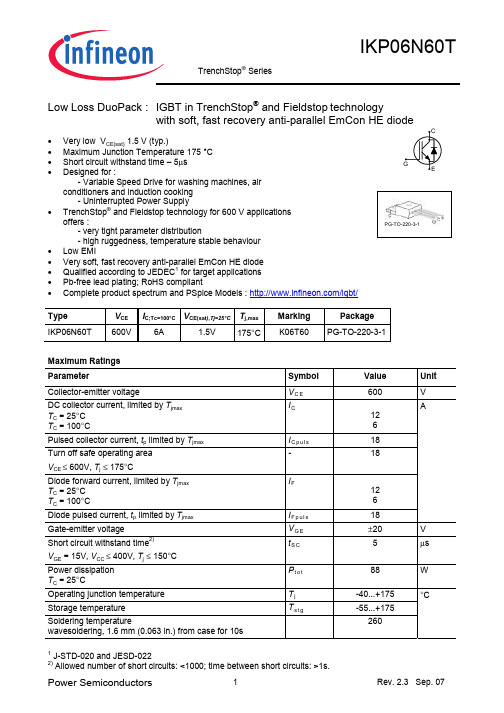
Low Loss DuoPack : IGBT in TrenchStop® and Fieldstop technologywith soft, fast recovery anti-parallel EmCon HE diode•Very low V CE(sat) 1.5 V (typ.)•Maximum Junction Temperature 175 °C•Short circuit withstand time – 5µs•Designed for :- Variable Speed Drive for washing machines, airconditioners and induction cooking- Uninterrupted Power Supply• TrenchStop® and Fieldstop technology for 600 V applicationsoffers :- very tight parameter distribution- high ruggedness, temperature stable behaviour• Low EMI•Very soft, fast recovery anti-parallel EmCon HE diode•Qualified according to JEDEC1 for target applications•Pb-free lead plating; RoHS compliant•Complete product spectrum and PSpice Models :/igbt/Type V CE I C;Tc=100°C V CE(sat),Tj=25°C T j,max Marking PackageIKP06N60T 600V 6A 1.5V 175°C K06T60 PG-TO-220-3-1Maximum RatingsParameter SymbolValueUnit Collector-emitter voltage V C E600 VDC collector current, limited by T jmax T C = 25°CT C = 100°C I C126Pulsed collector current, t p limited by T jmax I C p u l s18 Turn off safe operating areaV CE ≤ 600V, T j≤ 175°C-18Diode forward current, limited by T jmax T C = 25°CT C = 100°C I F126Diode pulsed current, t p limited by T jmax I F p u l s18AGate-emitter voltage V G E±20 VShort circuit withstand time2)V GE = 15V, V CC ≤ 400V, T j≤ 150°Ct S C 5 µsPower dissipationT C = 25°CP t o t88 W Operating junction temperature T j-40...+175Storage temperature T s t g-55...+175Soldering temperaturewavesoldering, 1.6 mm (0.063 in.) from case for 10s 260°C1 J-STD-020 and JESD-0222) Allowed number of short circuits: <1000; time between short circuits: >1s.PG-TO-220-3-1Thermal Resistance Parameter Symbol Conditions Max. Value UnitCharacteristicIGBT thermal resistance, junction – caseR t h J C 1.7 Diode thermal resistance, junction – case R t h J C D 2.6 Thermal resistance, junction – ambient R t h J A62K/WElectrical Characteristic, at T j = 25 °C, unless otherwise specifiedValueParameter Symbol Conditions min. typ. max. UnitStatic CharacteristicCollector-emitter breakdown voltage V (B R )C E S V G E =0V,I C =0.25mA 600 - - Collector-emitter saturation voltageV C E (s a t )V G E = 15V, I C =6A T j =25°C T j =175°C- - 1.5 1.8 2.05 Diode forward voltageV FV G E =0V, I F =6A T j =25°C T j =175°C - -1.6 1.62.05 -Gate-emitter threshold voltage V G E (t h ) I C =0.18mA, V C E =V G E 4.1 4.6 5.7V Zero gate voltage collector currentI C E S V C E =600V , V G E =0V T j =25°C T j =175°C- -- -40 700µAGate-emitter leakage current I G E S V C E =0V,V G E =20V - - 100 nA Transconductance g f s V C E =20V, I C =6A - 3.6 - S Integrated gate resistor R G i n tnone ΩDynamic Characteristic Input capacitance C i s s - 368 - Output capacitanceC o s s - 28 - Reverse transfer capacitance C r s s V C E =25V, V G E =0V, f =1MHz- 11 - pF Gate chargeQ G a t eV C C =480V, I C =6A V G E =15V- 42 - nCInternal emitter inductancemeasured 5mm (0.197 in.) from case L E - 7 - nH Short circuit collector current 1)I C (S C )V G E =15V,t S C ≤5µs V C C = 400V, T j = 25°C- 55 - A1)Allowed number of short circuits: <1000; time between short circuits: >1s.Switching Characteristic, Inductive Load, at T j =25 °CValueParameter Symbol Conditions min. typ. max. UnitIGBT Characteristic Turn-on delay time t d (o n ) - 9 - Rise timet r - 6 - Turn-off delay time t d (o f f ) - 130 - Fall time t f - 58 - ns Turn-on energy E o n - 0.09 - Turn-off energy E o f f - 0.11 - Total switching energyE t sT j =25°C,V C C =400V,I C =6A, V G E =0/15V, R G =23Ω, L σ2)=60nH, C σ2)=40pFEnergy losses include “tail” and diode reverse recovery.- 0.2 -mJ Anti-Parallel Diode Characteristic Diode reverse recovery time t r r - 123 - ns Diode reverse recovery charge Q r r - 190 - nC Diode peak reverse recovery current I r r m- 5.3 - A Diode peak rate of fall of reverse recovery current during t bdi r r /dtT j =25°C,V R =400V, I F =6A, di F /dt =550A/µs- 450 - A/µsSwitching Characteristic, Inductive Load, at T j =175 °CValueParameter Symbol Conditions min. typ. max. UnitIGBT Characteristic Turn-on delay time t d (o n ) - 9 - Rise timet r - 8 - Turn-off delay time t d (o f f ) - 165 - Fall time t f - 84 - ns Turn-on energy E o n - 0.14 - Turn-off energy E o f f - 0.18 - Total switching energyE t sT j =175°C,V C C =400V,I C =6A, V G E =0/15V, R G = 23Ω L σ1)=60nH, C σ1)=40pFEnergy losses include “tail” and diode reverse recovery.- 0.335 -mJ Anti-Parallel Diode Characteristic Diode reverse recovery time t r r - 180 - ns Diode reverse recovery charge Q r r - 500 - nC Diode peak reverse recovery current I r r m- 7.6 - A Diode peak rate of fall of reverse recovery current during t bdi r r /dtT j =175°C V R =400V, I F =6A, di F /dt =550A/µs- 285 - A/µs2) Leakage inductance L σ and Stray capacity C σ due to dynamic test circuit in Figure E.1)Leakage inductance L σ and Stray capacity C σ due to dynamic test circuit in Figure E.I C , C O L L E C T O R C U R R E N T100Hz1kHz10kHz100kHzI C , C O L L E C T O R C U R R E N T1V10V100V1000V0,1A1A10Af , SWITCHING FREQUENCYV CE , COLLECTOR -EMITTER VOLTAGEFigure 1. Collector current as a function ofswitching frequency(T j ≤ 175°C, D = 0.5, V CE = 400V, V GE = 0/+15V, R G = 23Ω) Figure 2. Safe operating area(D = 0, T C = 25°C, T j ≤175°C;V GE =15V)P t o t , P O W E R D I S S I P A T I O N25°C50°C 75°C 100°C 125°C 150°C0W 20W40W60W80WI C , C O L L E C T O R C U R R E N T0A5A10A15AT C , CASE TEMPERATURET C , CASE TEMPERATUREFigure 3. Power dissipation as a function ofcase temperature (T j ≤ 175°C)Figure 4. Collector current as a function ofcase temperature(V GE ≥ 15V, T j ≤ 175°C)I C , C O L L E C T O R C U R R E N T0V1V2V3V0A3A6A9A12A 15AI C , C O L L E C T O R C U R R E N T0V1V2V3V0A3A6A9A12A15AV CE , COLLECTOR -EMITTER VOLTAGEV CE , COLLECTOR -EMITTER VOLTAGEFigure 5. Typical output characteristic(T j = 25°C)Figure 6. Typical output characteristic(T j = 175°C)I C , C O L L E C T O RC U R R E N T0A3A6A9A12A15AV C E (s a t ), C O L L E C T O R -E M I T T S A T U R A T I O N V O L T A G E-50°C0°C 50°C 100°C0,0V0,5V1,0V1,5V2,0V2,5VV GE , GATE-EMITTER VOLTAGET J , JUNCTION TEMPERATUREFigure 7. Typical transfer characteristic(V CE =20V)Figure 8. Typical collector-emittersaturation voltage as a function of junction temperature (V GE = 15V)t , S W I T C H I N G T IM E S0A3A6A9A12A15At , S W I T C H I N G T I M E S10Ω30Ω50Ω70Ω90ΩI C , COLLECTOR CURRENTR G , GATE RESISTORFigure 9. Typical switching times as afunction of collector current (inductive load, T J =175°C,V CE = 400V, V GE = 0/15V, R G = 23Ω, Dynamic test circuit in Figure E) Figure 10.Typical switching times as afunction of gate resistor (inductive load, T J =175°C,V CE = 400V, V GE = 0/15V, I C = 6A, Dynamic test circuit in Figure E)t , S W I T C H I N G T I M E SV G E (t h ), G A T E -E M I T T T R S H O L DV O L T A G E-50°C0°C 50°C 100°C 150°CT J , JUNCTION TEMPERATURET J , JUNCTION TEMPERATUREFigure 11. Typical switching times as afunction of junction temperature (inductive load, V CE = 400V, V GE = 0/15V, I C = 6A, R G = 23Ω, Dynamic test circuit in Figure E)Figure 12. Gate-emitter threshold voltage asa function of junction temperature (I C = 0.18mA)E , S W I T C H I N G E N E R G Y L O S S E SE , S W I T C H I N G E N E R G Y L O S SE S10Ω30Ω55Ω80ΩI C , COLLECTOR CURRENTR G , GATE RESISTORFigure 13. Typical switching energy lossesas a function of collector current (inductive load, T J =175°C,V CE =400V, V GE =0/15V, R G =23Ω, Dynamic test circuit in Figure E) Figure 14. Typical switching energy lossesas a function of gate resistor (inductive load, T J =175°C,V CE = 400V, V GE = 0/15V, I C = 6A, Dynamic test circuit in Figure E)E , S W I T C H I N G E N E R G Y L O SS E SE , S W I T C H I N G E N E R G Y L O S S E S0,0m 0,1m 0,2m 0,3m 0,4m 0,5mT J , JUNCTION TEMPERATUREV CE , COLLECTOR -EMITTER VOLTAGEFigure 15. Typical switching energy lossesas a function of junction temperature(inductive load, V CE =400V,V GE = 0/15V, I C = 6A, R G = 23Ω, Dynamic test circuit in Figure E)Figure 16.Typical switching energy lossesas a function of collector emitter voltage(inductive load, T J = 175°C, V GE = 0/15V, I C = 6A, R G = 23Ω, Dynamic test circuit in Figure E)V G E , G A T E -E M IT T E R V O L T A G E0V5V10V15Vc , C A P AC I T A N C EQ GE , GATE CHARGEV CE , COLLECTOR -EMITTER VOLTAGEFigure 17. Typical gate charge(I C = 6 A)Figure 18. Typical capacitance as a functionof collector-emitter voltage (V GE =0V, f = 1 MHz)I C (s c ), s h o r t c i r c u i t C O L L E C T O R C U R R E N T12V14V 16V 18V0A 20A40A60A80At S C , S H O R T C I R C U I T W IT H S T A N D T I M E10V11V 12V 13V 14V0µs2µs4µs6µs8µs10µs12µsV GE , GATE -EMITTETR VOLTAGEV GE , GATE -EMITETR VOLTAGEFigure 19. Typical short circuit collectorcurrent as a function of gate-emitter voltage(V CE ≤ 400V, T j ≤ 150°C)Figure 20. Short circuit withstand time as afunction of gate-emitter voltage (V CE =600V , start at T J =25°C, T Jmax <150°C)Z t h J C , T R A N S I E N T T H E R M A L R E S I S T A N C E1µs10µs 100µs 1ms 10ms 100ms10-2K/W10-1K/W100K/WZ t h J C , T R A N S I E N T T H E R M A L R E S I S T A N C E1µs10µs 100µs 1ms 10ms 100ms10-210-1100t P , PULSE WIDTHt P , PULSE WIDTHFigure 21. IGBT transient thermal resistance(D = t p / T )Figure 22. Diode transient thermalimpedance as a function of pulse width (D =t P /T )t r r , R E V E R S E R E C O V E R Y T I M E0ns50ns100ns150ns200ns250nsQ r r , R E V E R S E R E C O V E R Y C H A R G E200A/µs400A/µs 600A/µs 800A/µsdi F /dt , DIODE CURRENT SLOPEdi F /dt , DIODE CURRENT SLOPEFigure 23. Typical reverse recovery time asa function of diode current slope (V R = 400V, I F = 6A,Dynamic test circuit in Figure E)Figure 24. Typical reverse recovery chargeas a function of diode current slope(V R =400V, I F =6 A,Dynamic test circuit in Figure E)I r r , R E V E R S E R E C O V E R Y C U RR E N T200A/µs 400A/µs 600A/µs 800A/µs0A2A4A6A8Ad i r r /d t , D I O D E P E A K R A T E O F F A L L O F R E V E R S E R E C O V E R Y C U R RE N Tdi F /dt , DIODE CURRENT SLOPEdi F /dt , DIODE CURRENT SLOPEFigure 25. Typical reverse recovery currentas a function of diode current slope(V R = 400V, I F = 6A,Dynamic test circuit in Figure E) Figure 26. Typical diode peak rate of fall ofreverse recovery current as a function of diode current slope (V R = 400V, I F = 6A,Dynamic test circuit in Figure E)I F , F O R W A R D C UR R E N T0V 1V 2V0A2A4A6A8A10AV F , F O R W A R D V O L T AG E0°C 50°C 100°C 150°C0,0V0,5V1,0V1,5V2,0VV F , FORWARD VOLTAGET J , JUNCTION TEMPERATUREFigure 27. Typical diode forward current asa function of forward voltageFigure 28. Typical diode forward voltage as afunction of junction temperaturePG-TO-220-3-1Leakage inductance Lσ =60nH and Stray capacity Cσ =40pF.Edition 2006-01Published byInfineon Technologies AG81726 München, Germany© Infineon Technologies AG 9/12/07.All Rights Reserved.Attention please!The information given in this data sheet shall in no event be regarded as a guarantee of conditions or characteristics (“Beschaffenheitsgarantie”). With respect to any examples or hints given herein, any typical values stated herein and/or any information regarding the application of the device, Infineon Technologies hereby disclaims any and all warranties and liabilities of any kind, including without limitation warranties of non-infringement of intellectual property rights of any third party.InformationFor further information on technology, delivery terms and conditions and prices please contact your nearest Infineon Technologies Office ().WarningsDue to technical requirements components may contain dangerous substances. For information on the types in question please contact your nearest Infineon Technologies Office.Infineon Technologies Components may only be used in life-support devices or systems with the express written approval of Infineon Technologies, if a failure of such components can reasonably be expected to cause the failure of that life-support device or system, or to affect the safety or effectiveness of that device or system. Life support devices or systems are intended to be implanted in the human body, or to supportand/or maintain and sustain and/or protect human life. If they fail, it is reasonable to assume that the health of the user or other persons may be endangered.。
Advantech ACP-1320MB 1U_上架式工业机箱 用户手册说明书

用户手册ACP-1320MB带双SATA存储托架、适用于ATX /mATX母板的1U上架式工业机箱版权声明随附本产品发行的文件为研华公司2009年版权所有,并保留相关权利。
针对本手册中相关产品的说明,研华公司保留随时变更的权利,恕不另行通知。
未经研华公司书面许可,本手册所有内容不得通过任何途径以任何形式复制、翻印、翻译或者传输。
本手册以提供正确、可靠的信息为出发点。
但是研华公司对于本手册的使用结果,或者因使用本手册而导致其它协力厂商的权益受损,概不负责。
认可声明ACP-1320MB、AIMB-766、AIMB-764、AIMB-762、AIMB-760、AIMB-750、AIMB-744、AIMB-742、AIMB-556和AIMB-554是研华公司的产品名。
所有其他产品名或商标均为各自所属方的财产。
在线技术支持如需技术支持与服务,请访问我们的技术服务网站:/supportPart No. 2002132011第二版中国印刷2009年6月ACP-1320MB用户手册ii安全指示1.请仔细阅读此安全操作说明。
2.请妥善保存此用户手册供日后参考。
3.用湿抹布清洗设备前,请从插座拔下电源线。
请不要使用液体或去污喷雾剂清洗设备。
4.对于使用电源线的设备,设备周围必须有容易接触到的电源插座。
5.请不要在潮湿环境中使用设备。
6.请在安装前确保设备放置在可靠的平面上,意外跌落可能会导致设备损坏。
7.设备外壳的开口是用于空气对流,从而防止设备过热。
请不要覆盖这些开口。
8.当您连接设备到电源插座上前,请确认电源插座的电压是否符合要求。
9.请将电源线布置在人们不易绊到的位置,并不要在电源在线覆盖任何杂物。
10.请注意设备上的所有警告和注意标语。
11.如果长时间不使用设备,请将其同电源插座断开,避免设备被超标的电压波动损坏。
12.请不要让任何液体流入通风口,以免引起火灾或者短路。
13.请不要自行打开设备。
为了确保您的安全,请由经过认证的工程师来打开设备。
编辑教你如何辨别什么是B3主板

○华硕B3步进P67/H67辨别方法
新版华硕P67/H67主板采用了全新的产品外包装,与上一代主板包装的最大区别就是在包装右上角印刷了“NEWH67B3Revision”标识。除此之外,型号下侧、包装四周都有相似的说明。
○微星B3步进P67/H67辨别方法
微星B3步进P67/H67在主板包装外部粘贴有“B3SteppingReady”标识,不过由于包装批次不同,有些主板包装的标识是粘贴的,有些则是直接印刷在产品包装上的。
数字的组合 小修改的重新流片一般都会只在原修订值中递增数字 如从A1到A2 若遇到大规模的或者非常重要的修改时
就会更改字母值 如从A1到B1 而本文中说的B2 其实就是指intel首批发布的6系列芯片组的修订信息值 而B3就是指修
正缺陷后 重新流片的6系列芯片的修订信息值 由此 我们也可以看出 B2芯片遇到的是个小问题 所以intel能如此迅速的
可能是由于批次不同,B3步进新版P67/H67主板的“新版6系列B3步进”有英文、中文两个版本,消费者在购买时只需认准B3即可。
○映泰B3步进P67/H67辨别方法B3步进版H67主板特别在主板包装上印刷了醒目的红色“B3VERSIONBUGFREE”标识。同时TH67+主板PCB版本号也升级到了Ver6.1。
片后就能毫无问题并上市的一般都会有一些工艺或者设计带来的大大小小的各种问题 工程师会对它进行多次检测 修
正并多次流片 每一次流片都会带来品质更好的芯片 例如BUG的修正 功耗的降低或者超频性能的提升等等 根据修改
程度的大小 芯片设计者都会相应的提升芯片步进和修订版本信息 以示区别 其中步进值多为纯数字 修订值多为字母加
到现在还是有很多人根本不懂什么叫步进 只是大致的了解了一下而已 而B2和B3的区别也完全不明白 好吧 我来专业的科普一下吧
G1.Sniper LGA1366主板 使用手册说明书

G1.SniperLGA1366主板支持Intel® Core™ i7 系列处理器使用手册Rev. 100112MSC-G1SNIPE-1001RFeb. 1, 2011Motherboard G1.Sniper Feb. 1, 2011Motherboard G1.Sniper目录清点配件 (6)选购配件 (6)G1.Sniper主板配置图 (7)G1.Sniper主板功能框图 (8)第一章硬件安装 (9)1-1 安装前的注意须知 (9)1-2 产品规格 (10)1-3 安装中央处理器及散热风扇 (13)1-3-1 安装中央处理器(CPU) (13)1-3-2 安装散热风扇 (15)1-4 安装内存条 (16)1-4-1 双通道/3通道内存技术 (16)1-4-2 安装内存条 (17)1-5 安装适配卡 (18)1-6 构建ATI CrossFireX™/NVIDIA SLI系统 (19)1-7 后方设备插座介绍 (20)1-8 内建指示灯 (22)1-9 插座及跳线介绍 (25)第二章BIOS 程序设定 (33)2-1 开机画面 (34)2-2 BIOS设定程序主画面 (35)2-3 MB Intelligent Tweaker(M.I.T.) (频率/电压控制) (37)2-4 Standard CMOS Features (标准CMOS设定) (47)2-5 Advanced BIOS Features (高级BIOS功能设定) (49)2-6 Integrated Peripherals (集成外设) (51)2-7 Power Management Setup (省电功能设定) (53)2-8 PC Health Status (电脑健康状态) (55)2-9 Load Fail-Safe Defaults (载入最安全预设值) (57)2-10 Load Optimized Defaults (载入最佳化预设值) (57)2-11 Set Supervisor/User Password (设定管理员/用户密码) (58)2-12 Save & Exit Setup (储存设定值并结束设定程序) (59)2-13 Exit Without Saving (结束设定程序但不储存设定值) (59)- 4 -第三章驱动程序安装 (61)3-1 芯片组驱动程序 (61)3-2 软件应用程序 (62)3-3 技术支持(说明) (62)3-4 与技嘉联系 (63)3-5 系统信息 (63)3-6 Download Center(下载中心) (64)3-7 新工具程序 (64)第四章独特功能介绍 (65)4-1 Xpress Recovery2介绍(一键还原) (65)4-2 BIOS更新方法介绍 (68)4-2-1 如何使用Q-Flash(BIOS快速刷新)更新BIOS (68)4-2-2 如何使用@BIOS(BIOS在线更新)更新BIOS (71)4-3 EasyTune 6介绍 (72)4-4 动态节能引擎™ 2 (Dynamic Energy Saver™ 2)介绍 (73)4-5 Q-Share介绍(极速共享) (75)4-6 Smart 6™介绍 (76)4-7 Auto Green介绍 (80)4-8 eXtreme Hard Drive (X.H.D)介绍 (81)4-9 Cloud OC介绍(云超频) (82)第五章附录 (83)5-1 如何构建Serial ATA硬盘 (83)5-1-1 设定Intel ICH10R SATA控制器模式 (83)5-1-2 设定JMicron JMB362 SATA控制器模式 (91)5-1-3 设定Marvell 88SE9182 SATA控制器模式 (97)5-1-4 安装SATA RAID/AHCI驱动程序及操作系统 (103)5-2 Bigfoot Killer 网络管理器 (115)5-3 音频输入/输出设定介绍 (116)5-3-1 2 / 4 / 5.1 / 7.1声道介绍 (116)5-3-2 S/PDIF输出设定 (117)5-3-3 Creative软件套件 (118)5-3-4 启动Dolby Digital Live/DTS Connect 编码 (119)5-3-5 录音设定 (121)5-4 疑难排解 (122)5-4-1 问题集 (122)5-4-2 故障排除 (123)5-5 管理声明 (125)- 5 -组上述附带配件仅供参考,实际配件请以实物为准,技嘉科技保留修改的权利。
产品说明书:UM-T W10 10寸内置2分频全频扬声器

TW1010寸内置2分频全频扬声器产品说明书CN UM-T W10-20180423Ve r B感谢您购买 产品!请仔细阅读本手册,它将帮助你妥善设置并运行您的系统,使其发挥卓越的性能。
并保留这些说明以供日后参照。
警告:为了降低火灾与电击的风险,请不要将产品暴露在雨中或潮湿环境中。
警告:为了降低电击的风险,非专业人士请勿擅自拆卸该系统。
仅供专业人士操作。
等边三角形中的闪电标记,用以警示用户该部件为非绝缘体,系统内部存在着电压危险,电压。
可能足以引起触电。
可能足以引起触电如系统标有带惊叹号的等边三角形,则是为提示用户严格遵守本用户指南中的操作与维护规定。
注意:请勿对系统或附件作擅自的改装。
未经授权擅自改装将造成安全隐患。
警告:燃不得将明火源(如点的蜡烛)放在器材上面。
1. 请先阅读本说明。
2. 保留这些说明以供日后参照。
3. 注意所有警告信息。
4. 遵守各项操作指示。
5. 不要在雨水中或潮湿环境中使用本产品。
6. 不要将产品靠近热源安装,例如暖气管、加热器、火炉或其它能产生热量的装置(包括功放机 )。
7. 不要破坏极性或接地插头的安全性设置。
如果提供的插头不能插入插座,则应当请专业人员更换插座。
8. 保护好电源线和信号线,不要在上面踩踏或拧在一起(尤其是插头插座及穿出机体以外的部分 )。
9. 使用厂商规定及符合当地安全标准的附件。
10.雷电或长时间不使用时请断电以防止损坏产品。
12. 不要让物体或液体落入产品内——它们可能引起火灾或触电。
13. 请注意产品外罩上的相关安全标志。
. 仅与厂商指定或与电器一同售出的推车、架子、三脚架、支架或桌子一起使用。
推动小车电/器时,应谨防翻倒。
11注意事项产品的安装调试须由专业人士操作。
在使用非本厂规定的吊装件时,要保证结构的强度并符合当地的安全规范。
警告:1扬声器及扬声器系统的产品有限保修期为自正式购买日起的3年。
由于用户不合理的应用而导致音圈烧毁或纸盆损坏等故障,不包含于产品保修项目。
MB1-10AP 用户手册说明书

User ManualV1.4 M aster Series Embedded SystemIntel ® Apollo Lake ProcessorsEfficient, Versatile, and Rugged & ReliablePREFACECopyright NoticeCopyright © 2016-2020 MiTAC Computing Technology Corporation (MiTAC Group). No part of this document may be reproduced, copied, translated, or transmitted in any form or by any means, electronic or mechanical, for any purpose, without the prior written permission of MiTAC Corp., Ltd. All information and specification provided in this manual are for reference only and remain subject to change without prior notice.DisclaimerWe reserve the right to make changes, without notice, to any product, including circuits and/or software described or contained in this manual in order to improve design and/or performance. We assume no responsibility or liability for the use of the described product(s) conveys no license or title under any patent, copyright, or masks work rights to these products, and make no representations or warranties that these products are free from patent, copyright, or mask work right infringement, unless otherwise specified. Applications that are described in this manual are for illustration purposes only. We make no representation or guarantee that such application will be suitable for the specified use without further testing or modification.Declaration of ConformitySafety InformationSafety PrecautionsFor your safety, please carefully read all the safety instructions before using the device. All cautions and warnings on the equipment should be noted. Keep this user manual for future reference.*Let service personnel to check the equipment in case any of the following problems appear:⏹The power cord or plug is damaged.⏹Liquid has penetrated into the equipment.⏹The equipment has been exposed to moisture.⏹The equipment does not work well or you cannot get it to work according to the user manual.⏹The equipment has been dropped and damaged.⏹The equipment has obvious signs of breakage on the surface.Ordering InformationPacking ListOptional Xpansion Modules MS-01DVI-D10MS-01DPN-D10MS-02COM-D10MS-08DIO-T10CONTENTSPREFACE (2)CHAPTER 1: INTRODUCTION (8)1.1 Overview (8)1.2 Product Features (8)1.3 Hardware Specification (9)1.4 Mechanical Specification (12)1.5 System I/O Placement (13)CHAPTER 2: DIP SWITCH SETTING AND PIN DEFINITION (16)2.1 DIP Switch and Connector Overall Placement (16)2.2 DIP Switch Setting (18)2.3 Connector Pin Definition (19)CHAPTER 3: SYSTEM SETUP (26)3.1 2.5” SATA HDD/SSD Installation (26)3.2 WiFi module Installation (27)3.3 DRAM Installation (28)CHAPTER 4: BIOS SETUP (31)4.1 Main Page (31)4.2 Advance Page (33)4.3 Security Page (42)4.4 Boot Page (46)4.5 Save & Exit Page (47)INTRODUCTIONThis chapter provides the MB1-10AP EmbeddedSystem product overview, including features, hardware and mechanical specifications. 1CHAPTER 1: INTRODUCTIONThis chapter provides the MB1-10AP Embedded System product overview, including features, hardware, mechanical specifications, and I/O placement.1.1 OverviewMiTAC’s MB1-10AP embedded system is the next generation embedded system with Intel® Apollo Lake embedded processor. The efficient performance, OCP/OVP power protection, and expandable design provide the solution for routine tasks and most types of application.1.2 Product FeaturesMB1-10AP Embedded System offers the following features:⏹Intel® Apollo Lake-M N3350/N4200 Processors⏹Support 2 x PoE LAN (Optional)⏹Support HDMI as primary display, and VGA/DisplayPort/DVI-D as second option⏹Fan-less chassis and Expandable module design⏹Support COM/DIO via Xpansion Modules⏹8-24V Wide Power Voltage⏹-25°C to 70°C (For non-PoE SKU, with 0.7m/s Air Flow and Wide TemperatureMemory/Storage)-25°C to 60°C (For PoE SKU, with 0.7m/s Air Flow and Wide TemperatureMemory/Storage)1.3 Hardware Specification*Notes1: Installation in Restricted Access Location (RAL)A restricted access location is a designated area within an incident area (High or Low temperature environment)With authorized people can enter for a period of time and for a specific purpose.1.Access can only be gained by service people or by users who have beeninstructed about the reasons for the Restrictions applied to the location and about any precautions that shall be taken.2.Access is through the use of a tool or lock and key, or other means ofsecurity, and is controlled by the authority Responsible for the location.*Notes2: Please make sure that the power consumption is in the spec of the power supply output capability from AC adaptor (72W or 120W). Please choose the suitable AC adaptor for your application.AC/DC 24V/5A, 120W 3PIN Terminal Block Power Adaptor (For PoE SKU)AC/DC 24V/3A, 72W 3PIN Terminal Block Power Adaptor (For non-PoE SKU)*Note3: Please choose 120W AC adaptor for the Optional Xpansion Module (MS-02COM-D10) COM ports in maximum power loading scenario (12V max. 1A loading).*Note4: Please don’t load the COM power in the hardware configuration and high temperature condition. Don’t operate the machine at maximum operating temperature 70℃(Non-PoE SKU) & 60℃(PoE SKU) with 4*COM 12V*1A loading.*Note 5: The maximum ambient operating temperature is 40°C if the external AC adapter model: EA11011M or EA10681V will be placed in thesame high temperature area with the embedded system.*Note 6: CAUTION - Lithium battery is included in this embedded system. Please do not puncture, mutilate, or dispose of battery in fire. There will be danger of explosion if battery is incorrectly replaced. Replace only with the same or equivalent type recommended by manufacturer. Dispose of used battery according to manufacturer instructions and in accordance with your local regulations.*Note 7: CAUTION - Only allow technically qualified personnel to touch the I/O surface, and only when the unit is well fastened by wall mount, VESA mount, or DIN Rail mount. Please also avoid to contact the I/O surface more than 1 second in high temperature and harsh environment. Not allow to touch aluminum alloy surface at high temperature. The technically qualified personnel also needs to have technical knowledge, operating experiences, and basic knowledge about MB1-10AP product spec.1.4 Mechanical SpecificationMechanical Dimension: 170 mm x 105 mm x 57 mm1.5 System I/O Placement⏹Front I/O:⏹Rear I/O:Xpansion Module (Optional) ConfigurationDIP SWITCH SETTING AND PIN DEFINITIONThis chapter provides information about how to set up thedip switch and use I/Os of MB1-10AP Embedded System hardware. 2CHAPTER 2: DIP SWITCH SETTING AND PIN DEFINITIONThis chapter provides information about how to set up the dip switch, and use internal I/Os of MB1-10AP Embedded System hardware.2.1 DIP Switch and Connector Overall PlacementFront View:Bottom View:2.2 DIP Switch Setting⏹Location #B6ATATX A SW_ATX1CAdd this table in silkscreen TXTDefault ATX mode⏹ Location #B7/B8/B9/B102.3 Connector Pin Definition⏹ Indicator for Realtek RTL8154B LAN⏹ Location #B4 – SATA and SATA PWR Connector3-pin terminal block for DC Input⏹2-pin Remote Power On/Off HeaderMB Side Connector: Molex 151064-0152Suggestive Cable Side Plug: Molex 151100-0002⏹COM1 and COM2 on M/BMB COM1 and COM2 RS232, RS422, RS485 setting is at BIOS setup menuMS-02COM-D10 (Optional)Xpansion Module with 2 x RS232/422/485 (Non-isolation)Support 5V/12V DC Power OutputNotes: Don't support Power HOT switch at SW_PW3 and SW_PW4 in Xpansion Module Below is Xpansion Module with COM3 and COM4: See the power RS232 setting as below table:Default setting is RI signal at A location from SW_RI3 and SW_RI4Power COM setting with RI signal: Default settingSET at A location from SW_RI3 and SW_RI4SET at A location from SW_PW3 and SW_PW4Power 5V setting:SET at C location from SW_RI3 and SW_RI4 SET at A location from SW_PW3 and SW_PW4Power 12V setting:SET at C location from SW_RI3 and SW_RI4 SET at C location from SW_PW3 and SW_PW4Power 12V setting: Change at C location from SW_RI3 and SW_RI4 and at C location from SW_PW3 and SW_PW4MS-08DIO-T10 (Optional)Xpansion Module with 8-bit Optical Isolation DIDO (4 x DI, 4 x DO)SYSTEM SETUPThis chapter provides information about how to set up the MB1-10AP Embedded System hardware installation. 3CHAPTER 3: SYSTEM SETUPThis chapter provides information about how to set up the MB1-10AP Embedded System hardware installation.3.1 2.5” SATA HDD/SSD InstallationPlease follow the instructions to install SATA HDD as below. - Loosen 6 screws from Bottom cover as the arrow locations- Loosen 4 screws as the arrow directions-Move HDD tray as arrow direction-Lift HDD tray about 45 degrees and draw it out-Install 2.5”HDD to the HDD tray3.2 WiFi module Installation-Use mPCIe extension bracket which is in accessories kit to fix half size mPCIe wifi module, and install to the full size mPCIe slot3.3 DRAM Installation-Loosen 4 screws from MB (2 screws from front & rear cover)-Draw the MB sub-assembly out from top cover as arrow direction-Remove the film from top cover & install DIMM to MBBIOS SETUPThis chapter provides information about how to set up BIOS and use BIOS menu items to adjust basic function settings. 4CHAPTER 4: BIOS SETUPThis chapter provides information about how to set up BIOS and use BIOS menu items to adjust basic function settings.4.1 Main Page4.2 Advance Page4.2.1 Intel(R) I210 Gigabit Network Connection4.2.2 Trusted Computing4.2.3 NCT6116D Super IO Configuration4.2.4 Hardware Monitor4.2.5 S5 RTC Wake Setting4.2.6 CPU Configuration4.3 Security Page4.3.1 Secure Boot4.3.2 BIOS Update4.4 Boot Page4.5 Save & Exit Page。
XSB SL系列主板安装指南说明书

Ground =::::H"n� � Fan Header= ""'8 Pin 12v PowerConnector Pin Si nalFront Audio Connector 121 2 33 4 455 6 677 8 89 10 910ConnectorSPDIF2 4 61 3 5SV3A.Advanced RMA:PORT1 LAUO GNOPORT1_RPRECENCEJPORT2 RSENSE1 RETURNSENSE_SENOEmPORT2 LSENSE2 RETURNPin Definition23456PowerNo PinSPDIFSPDIFIOROUNDGROUNDGround Ground12V 12VSense SensePremium ServicesProtect yourself and accelerate the RMA process./EAR1 + 1 Warranty:Register the purchased product within 30 days to receive2 year warranty./warrantyCMOSPowerButtonResetButtonConnector PinFanHeaderSi nalIEEE 1394a Connector f---'1--+--"TP'--'-A-"-+----l2 4 6 8 10•• •• •• •• •1 3 5 7 9MODS RIGS:2 T P A-3 GND4 GND5 TPB+6 TPB·7 + 12V8 + 12V9 Empty10 GNDShow off your rig, post your specs, submit your score,and win big.CPU Fan Header '":�::�J IGround24 Pin ATX PowerRX·RX+GN D GN DSATA Ports IPost LEDPWRLED PWRSW Blank+2 109+HD_LED RESET NoConnectConnector Pin Si!J1al Pin SignalU SS 2.0 Header connector t-'-1-+'5V�D�U�A l c..+=2--+�5V�DU��L---i13579 3 D· 4 D-0+■■ ■ ••■• ■■2 4 B 8 105 D+ 67 GN D B GN D9 Em 10 No ConnectSV3A. SoftwareE-LEET:Easily push the boundaries of your hardware with thisexclusive tuning utility./eleet1)(·1)(+GN DPlease see the manual for more details.1 . PS/2 Keyboard Port 4.Optical SPDIF OutputB 2.0 Ports N Ports (10/100/1000)3.Coaxial SPDIF Output 6.Audio Ports■One DIMM: If using 1 DIMM (Slngle Channel),install into: DIMM slot 1.■Two or Four DIMMs: If using 2 DIMMs (Dual Channel),install into: DIMM slots 1 and 3. If using 4 DIMMs(Dual Channel), install into: DIMM slots 2, 1, 4, and 3.■Three DIMMs: If using 3 DIMMs (Trlple Channel),install into: DIMM slots 1, 3, and 5.■Six DIMMs: If using more than 4 DIMMs, use:DIMM slots 2, 1, 4, and 3 then proceed to occupythe following DIMM slots in this order: 5 and 6.ATTENTION:EVGA recommends applying 1.65V or less whensetting the DIMM Voltage. This will support longterm stability.SV3A. SupportTechnical Support888 • 881 · EVGA ·2717 North America only/about/contactus/Thank you for purchasing an EVGA product.Please remember to register your product at:/registerFor the latest drivers and updates for yourproduct p l ease visit:/support/drlversTo visit and search our knowledge base andproduct FAQ please visit:/FAQTo visit the EVGA community messageboards please visit:For more information about these servicesas well as our terms and conditions please visit。
映泰科技主板说明书

ASRock DuraCap (2.5 x longer life time), 100% Japan made high quality conductive polymer capacitors Digi Power, Supports AM3+ Processor, 8-Core CPU Supports Dual Channel DDR3 2100(OC) Supports AMD Quad CrossFireX™, 3-Way CrossFireX™ and CrossFireX™ Supports NVIDIA® SLI™ 4 x USB 3.1 Gen1, 5 x SATA3, 2 x IEEE 1394, Dr. Debug, Power/Reset/Clear CMOS Switch with LED 7.1 CH HD Audio with Content Protection (Realtek ALC892 Audio Codec) Supports ASRock XFast RAM, XFast LAN, XFast USB Technologies Supports Graphical UEFI, On/Off Play, Instant Boot, Instant Flash, APP Charger, Turbo UCC, APP Shop Free Bundle : CyberLink MediaEspresso 6.5 Trial This model may not be sold worldwide. Please contact your local dealer for the availability of this model in your region. - Support for Socket AM3+ p
- 1、下载文档前请自行甄别文档内容的完整性,平台不提供额外的编辑、内容补充、找答案等附加服务。
- 2、"仅部分预览"的文档,不可在线预览部分如存在完整性等问题,可反馈申请退款(可完整预览的文档不适用该条件!)。
- 3、如文档侵犯您的权益,请联系客服反馈,我们会尽快为您处理(人工客服工作时间:9:00-18:30)。
6.1
驱动程序安装注意事项 ...................................................................36
6.2
附加信息 ...........................................................................................37
SATA 2 & 3 集成串行ATA控制器
数据传输率为3.0 Gb/s / 6.0 Gb/s 符合SATA 2.0 / 3.0 规范
网络
Realtek RTL 8111E
10 / 100 Mb/s / 1Gb/s自适应传输模式 半双工/全双工工作模式
音效
ALC892
6声道音频输出 支持高清音频
USB3.0
第二章: 硬件安装 ........................................................... 5
2.1
中央处理器(CPUຫໍສະໝຸດ ..............................................................................5
1.4
后置面板接口 .....................................................................................3
1.5
主板布局图 .........................................................................................4
CPU
Socket 1155 Intel Core i7 / i5 / i3 / Pentium / Celeron处理器
支持硬件防病毒功能 / 增强型 Intel SpeedStep技术 / Intel 64位体系结构 / 64位内存扩展技术 / 虚拟技术 / 超线程技术
芯片组
Intel P67
IT8728 高级I/O控制器 提供最基本的I/O功能
第五章: T系列UEFI BIOS和软件 .................................. 23
5.1
T系列UEFI BIOS .............................................................................23
本用户手册的所有内容若有任何错误,制造商没有义务为其承担任何责任。所有 商标和产品名称均有其各自所有权。
未经过书面许可,不得以任何形式(部分或全部)复制此手册信息。
免责说明
本手册内容系BIOSTAR®知识产权,版权归BIOSTAR®所有。我们本着对用户负 责的态度,精心地编写该手册,但不保证本手册的内容完全准确无误。BIOSTAR® 有权在不知会用户的前提下对产品不断地进行改良、升级及对手册内容进行修正, 实际状况请以产品实物为准。本手册为纯技术文档,无任何暗示及影射第三方之 内容,且不承担排版错误导致的用户理解歧义。本手册中所涉及的第三方注册商 标所有权归其制造商或品牌所有人。
T P 6 7 B + 设置手册
FCC 条款
依照 FCC 条款第 15 部分的规定,本装置已经通过测试并且符合 Class B 级数字 装置的限制。此条款限制了在安装过程中可能造成的有害射频干扰并提供了合理 的防范措施。本装置在使用时会产生无线射频辐射,如果没有依照本手册的指示 安装和使用,可能会与无线通讯装置产生干扰。然而,并不保证在特定的安装下 不会发生任何干扰。
4.2
RAID阵列..........................................................................................19
4.3
RAID运行..........................................................................................19
1.2
附件 .....................................................................................................1
1.3
主板特性 .............................................................................................2
5.2
T系列软件 ......................................................................................... 26
第六章: 帮助信息 .......................................................... 36
CE 符合性简短声明 我们声明此产品符合现行法律,并满足 2004/108/CE, 2006/95/CE 和 1999/05/CE 的指令规定的所有基本要求。
T P 6 7 B + 设置手册
防静电操作规则
静电可能严重损坏您的设备,在处理主板以及其它的系统设备的时候要特别注意, 避免和主板上的系统组件的不必要接触,保证在抗静电的环境下工作,避免静电 放电可能对主板造成损坏,当在您的机箱中插入或者移除设备时,请保证电源处 于断开状态,厂商对于不遵照本操作规则或者不遵守安全规范而对主板造成的损 坏不负责。
目录
第一章: 主板介绍 ........................................................... 1
1.1
前言 .....................................................................................................1
2.2
风扇接头 .............................................................................................7
2.3
系统内存 .............................................................................................8
低管脚数接口
环境控制 H/W 监控 风扇速度控制器 ITE's "智能保护" 功能
主内存
DDR3 DIMM 插槽 x 4 最大内存容量为16GB 每个DIMM支持512MB/1GB/2GB/4GB DDR3
双通道模式 DDR3内存模组 支持DDR3 1066 / 1333 支持DDR3 1600 (OC) / 1866 (OC) / 2133 (OC) 不支持Registered DIMM和ECC DIMM
x1
支持 PCI-E Gen2 x1扩展卡
板载接口
SATA3接口
2.4
接口和插槽 .......................................................................................10
第三章: 接头和跳线安装............................................... 14
6.3
问题解答 ...........................................................................................38
目录
UEFI BIOS设置 ............................................................ 39 1 主菜单........................................................................ 41 2 高级菜单 .................................................................... 42 3 芯片组菜单................................................................. 51 4 系统引导菜单 ............................................................. 54 5 安全菜单 .................................................................... 55 6 O.N.E系列菜单 .......................................................... 56 7 退出菜单 .................................................................... 61 附:产品中有毒有害物质或元素的名称及含量 ............. 62
NEC uPD720200
数据传输率为600 MB/s
PCI 插槽
x2
支持 PCI 扩展卡
PCI-E Gen2 x16 @ x16 插槽
x1
支持 PCI-E Gen2 x16扩展卡
插槽
PCI-E Gen2 x16 @ x4 插槽
x1