opto couple
电源安规设计规范

超音波焊接外壳的内部到外部安全距离测量方法:如右图,中间 突出部分比较宽在超音波焊接时不会融化,正确的电气间隙和爬 电距离尺寸为红色虚线所示,设计时应注意。
R/I 输出线在施加10N作用力下与任何带危险 电压的零部件间距离必须满足Cl:6.0mm/Cr:6.0mm Min.,如距离不足可使用 热缩套管或固定线材的方式增加绝缘距离.
B/I Fuse 前L-N间或Fuse引脚间,fuse前与fuse后,按照设 备输入电压设计适当的安全距离。一般设计要求为: Cl:3.0mm/Cr:3.0mm Min.
B/I 一次侧线路与保护接地导体间,按照设备输入电 压设计适当的安全距离。一般设计要求为: Cl:3.0mm/Cr:4.0mm Min.
绕组温升要求(IEC60950-1&GB4943-2011) :
绝缘等级
Class A Class E Class B Class F Class H
最高温升限制ΔT(K)
75 90 95 115 140
最高温度限制(℃)
100 115 120 140 165
异常状况下最高温度限制 (℃)
150 165
危险能量
• 设计要点:输出端子设计成不能被测试指桥接的形式,或将输出 能量限制在持续1minute最大输出小于240VA。
SELV电路
• 设计要点: • 1.在正常工作时,SELV电路电压不应超过安全电压或60Vdc)。 • 2.在单一故障条件下,经过后,电压不应超过安全电压或60Vdc),
而且其极限值不应超过71Vpeak或120Vdc。
175 190 210
注:⑴上表中温带是以室温25℃为基础,对热带是以35℃为基准;
⑵如果以热电耦偶合式量测,则最大温升限值需减10℃。
可靠性预计 电信 电子
FOREWORD
This present databook gives elements to calculate failure rate of mounted electronic components. It made easier equipment reliability optimization studies, thanks to influence factors introduction. This document replaces and cancels UTE C 80 - 810 (June 1997). This present guide has been adopted on 07/03/2000 by the UTE board of directors.
76 à 77 77 77 77 78 à 89 79 à 81 82 à 83 84 à 85 86 à 87 88 à 89 90 à 91 91 92 à 93 93 93 93 93 94 à 95 95 95 95 95 96 à 97 97 97 97 97 98 à 99 99 99 9TE
This reliability calculation guide for electronic and optical card, is an important progress compared to older guides. Calculation models take directly into account the influence of the environment. The thermal cycling seen by cards, function of mission profiles undergone by the equipment, replace environment factor which is difficult to evaluate. These models can handle permanent working, on/off cycling and dormant applications. On the other hand, failure rate related to the component soldering, is henceforth included in component failure rate.
IPMIGBT的应用问题含电路,布线设计

1.0E+07
Power Cycle of IPM (以DIP IPM为例)
1% 10%
1.0E+06
0.1%
Failure probability
Power cycle
1.0E+05
DIP-IPM power cycle is greatly effected by the junction temperature variation ∆Tj. To ensure a large power cycle with less failure probability, it is necessary to avoid steep temperature swing of chip temperature.
All Mitsubishi IGBT-Modules have square switching SOA up to double rated current
i
2xIc
Conditions:
collector current
Ic
2 VCC ≤ VCES 3
RG (min) ≤ RG ≤ 10 × RG (min)
1,000,000,000
NF series (under comfirmation)
100,000,000
Number of Cycles
10,000,000
F series
1,000,000
H series
100,000
Failure ratio;1%
10,000
1,000 1 10 Δ Tj [℃] 100 1000
ICP
t
Two module selection criteria
电子信息科学类专业必备英语单词_

access: 读写;接入active: 有源的;有效的adaptor: 适配器address: 地址addressing: 寻址aerial: 天线* algorithm: 算法Ampere: 安培amplify: 放大* amplifier: 放大器amplitude: 幅度analog: 模拟的analog-to-digital converter: 模数转换器* antenna: 天线array: 阵列assembly: 组件assembly language: 汇编语言asynchronous: 异步的attenuation: 衰减* automation: 自动化backup: 备份* band: 波段;频段barcode: 条形码base: 基础;基极baseband: 基带* battery: 电池baud: 波特beam: 波/光束* binary: 二进制bipolar: 双极性bitmap: 位图Bluetooth: 蓝牙技术Boolean: 布尔型的;逻辑类型的boot: 引导;启动breakdown: 击穿brightness: 亮度buffer: 缓冲器* bus: 总线buzzer: 蜂鸣器bypass: 旁路* cable: 电缆* capacitor: 电容器capacitance: 电容(值)case: 封装;大小写case-sensitive: 区分大小写的casing: 封装* carrier: 载波cell: 电池;单元* cell phone: 手机cellular phone: 蜂窝电话cache: 高速缓存* channel: 信道;频道;通道* chip: 芯片* circuit: 电路* code: 码;代码;编码* source codes: 源代码codec: 编码解码器coding: 编码collector: 集电极* clock: 时钟* communication: 通信; 交通compatible: 兼容的compensation: 补偿competition: 竞争* compile: 编译compiler: 编译器complex: 复数* component: 元器件;成分* computer: 计算机concurrency: 并发* conductor: 导体* connector: 连接器;插接件console: 控制台constant: 恒定的* consumable: 耗材* consumer electronics: 消费类电子(产品) converter: 转换器* counter: 计数器couple: 耦合cordless phone: 无绳电话crosstalk: 串音;交叉干扰* crystal: 晶体* current: 电流* cursor: 光标cutoff: 截止cyberspace: 网络空间;虚拟空间cutter: 剪子;(剪线)钳子data: 数据* debug: 调试程序;除错* decimal: 十进制的;小数点的decupling: 去耦default: 缺席;默认值definition: 清晰度;分辨力* demodulation: 解调* design: 设计detection: 检波;解调;探测device: 设备;元件die: 晶片;晶粒;小片dielectric: 电介质的;绝缘的* digital: 数字的;数码的* diode: 二极管direct-coupled: 直接耦合的discrete: 分离的;分立的discrimination: 分辨率;识别力distributed: 分布式的document: 文件domestic appliances: 家用电器drift: 漂移drive: 驱动* driver: 驱动器;驱动程序dual-in-line: 双列直插duplex: 双工edge: 边沿edit: 编辑* electricity: 电;电流;电学electric: 电的;导电的;用电的;电动的* electrical: 电的;电气科学的electrician: 电工electron: 电子* electronic: 电子的* electronics: 电子学electromagnetic field: 电磁场electromagnetic waves: 电磁波embedded system: 嵌入式系统emitter: 发射极encryption: 编密码;加密entropy: 熵envelop: 包络equalization: 均衡equation: 方程* equipment: 设备Ethernet: 以太网fabrication: 制造;组装fade: 衰落facsimile: 传真feedback: 反馈* filter: 滤波器firewall: 防火墙firmware: 固件(存储在只读存储器中的软件)flash memory: 闪存frame: 帧* frequency 频率* fuse: 保险丝* gain: 增益gateway: 网关generator: 发电机;发生器* glass fiber: 玻璃纤维hacker: 黑客* image: 图像* impedance: 阻抗impulse: 冲激* inductor: 电感器inductance: 电感(量)* information: 信息infrastructure: 基础设施* input: 输入integer: 整型数* integrated circuit: 集成电路(芯片);IC interactive: 交互式的* interface: 接口* interrupt: 中断inverter: 反向器;非门* information technology: 信息技术; IT jamming: 干扰* laser: 激光layout: 布置;布局lead: 1. 引线;连线;2.铅line: 线路link: 连接;链路;* load: 负载magnitude: (复数的)模;幅度manufacture: 制造matrix: 矩阵measure: 测量;测度;措施* measurement: 测量mechatronics: 机电一体化;机械电子学* message: 消息meter: 仪表microcontroller: 微控制器* microphone: 麦克风* microprocessor: 微处理器* microwave: 微波* mobile phone: 移动电话model: 模型;型号module: 模块;组件modulate: 调制* modulation: 调制* modem: 调制解调器* monitor: 监视器* motor: 电动机;马达;汽车;汽艇* multimedia: 多媒体multiplex: 多路复用mutual conductance: 互导* network: 网络networked computing: 网络计算* noise: 噪音nominal: 标称的;名义上的offset: 补偿;偏离open circuit: 开路* optical fiber: 光学纤维opto-: 光-oscillation: 振荡* oscillator: 振荡器* oscilloscope: 示波器* output: 输出overflow: 溢出overhead: 开销overload: 1. 过载;2.重载package: 包* phase: 相位pin: 管脚pliers: 钳子;老虎钳;手钳plotter: 绘图仪* plug: 插头polarization: 极化potentiometer: 电位器* power: 功率;动力* power supply: 电源* printer: 打印机probe: (示波器)探头process: 过程;进程processing: 处理* programme: 程序projector: 投影仪* pulse: 脉冲quartz: 石英radar: 雷达* radio: 1. 无线电传送real time: 实时receive: 接收* receiver: 接收机* record: 记录rectifier: 整流器;检波器* relay: 继电器;中继;转播;refresh: 刷新register: 注册;寄存器* regulator: 稳压器* remote sensing: 遥感resin: 松香resistance: 电阻(量)* resistor: 电阻(器) resolution: 分辨率;解析率resonate: 谐振response: 响应route: (PCB)布线router: 路由器sample: 样本;样品;采样* satellite: 卫星saturation: 饱和scan: 扫描* scanner: 扫描仪;天线* screen: 1. 屏幕;2. 屏蔽screw: 螺丝钉screwdriver: 螺丝刀* semiconductor: 半导体serial no: 序列号series: 级数;串联set top box: 机顶盒sharing: 共享shielding: 屏蔽short circuit: 短路* signal: 信号* silicon: 硅simulation: 模拟* software: 软件* socket: 插座solder: 焊锡;焊接source: 源;源极* spare: 备件* spectrum 谱;频谱* specification: 指标storage: 存储* switch: 开关;交换synchronism: 同步* system: 系统* technology: 技术* telecommunication: 电信* telegraph: 电报* telephone: 电话* television: 电视* terminal: 终端;集散地* transformer: 变压器* transistor: 晶体三极管* transmission: 传输* transmitter: 发射机* transportation: 运输trig: 触发tune: 调谐update: 更新upgrade: 升级vacuum tube: 真空管;电子管* video: 视频Volt: 伏特* voltage: 电压wafer: 晶片;硅片;晶圆Watt 瓦特wave: 波waveform generator: 波形发生器waveguide: 波导wavelength: 波长wire: 线;导线* wireless: 无线的adder 加法器and gate 与门audio amplifier 音频放大器comparator 比较器DC-coupled 直流耦合的flip-flop 触发器mixer 混合器,混频器modulator 故障,失灵opertional amplifier 运算放大器radio frequency amplifier 射频放大器superconductiong 超导电的video amplifier 视频放大器zener diode 稳压二极管active element 有源元件anode 阳极attributable 可归属的bais 偏压cathode 阴极current intensity 电流强度dope 掺杂electrode 电极field-effect transistor 场效应管grid 格子,栅极magnetic field 磁场monolithic 独石的,整体的,单片的passive component 无源元件photocell 光电管光电池sensor 传感器triode 三极真空管unipededly 无阻的,不受阻的abstract code 抽象码acronym 缩写字assembler 汇编程序,汇编器assembly language 汇编语言bit (二进制)位,比特bug 故障,错误byte 字节,位元组central processing unit 中央处理器decoder 译码器graghical user interface 图形用户界面icon 图标,像标instruction register 指令寄存器machine code 机器码menory location 存储单元program counter 程序计数器专业英语词汇静态电阻(n.) static resistance 2.动态电阻(n.)dynamic resistance 3.感抗(n.) inductive reactance 4.容抗(n.) capacitive reactance 5. 阻抗(n.) impedance 6. 导纳(n.) admittance 7. 电子电路(n.) electronic circuitry 8. 二端元件(n.) two-terminal element 9. 电压降(n.) voltage drop 10. 毫安(n.) milliampere 11.微伏(n.) microvolt 12.纳米(n.) nanometer 13皮法(n.) picofarad 14千克(n.) kilogram 15兆欧(n.) megohm 16电介质(n.) dielectric 17线圈(n.) coil18磁场(n.) magnet field19电场(n.) electric field20电荷守恒(n.) electric charge conservation / conservation of electric charge21节点(n.) node22回路(n. ) loop23正极(n.) positive polarity / anode 24负极(n.) negative polarity / cathode 25三角函数(n.) trigonometric function 26正弦(n.) sine27余弦(n.) cosine 28阶跃函数(n.) step function29脉冲函数(n.) impulse function30静态响应(n.) static response 31稳态过程(n.) steady process32瞬态分析(n.) transient analysis33时变的(adj.) time-variant34是不变的(adj.) time-invariant35频域(n.) frequency domain36时域(n.) time domain37超前网络(n.) lead network38滞后网络(n.) lag network39频带宽度(n.) bandwidth 40半导体(n.) semiconductor 41微波(n.) microwave42声纳(n.) SONAR(sound navigation and ranging)43雷达(n.) RADAR(radio detecting and ranging)44只读存储器(n.) ROM(read only memory)45随机(存取)存储器(n.) random access memory46交流电(n.) AC(alternating current)47直流电(n.) DC(direct current)48发光二极管(n.) LED(light emitting diode)49正电子(n.) positron50负电子(n.) negatron 51变压器(n.) transforme52接收机(n.) receiver 53发射机(n.) transmitter 54放大器(n.) amplifier 55本振器(n.) local oscillator56滤波器(n.) filter 57混频器(n.) mixer 58解调器(n.) demodulator 59衰减器(n.) attenuator 60锁相环合成器(n.) phase-locked loop synthesizer 61检波器(n.) detector 62反相器(n.) inverter 63窄带的(n.) narrow-band 64旁(频)带(n.) sideband 65差频(n.) difference frequency 66和频(n.) sum frequency 67中频(n.) intermediate frequency 68射频, 无线电频率(n.) Radio Freqency 69次要频率(n.) second frequency 70噪声系数[指数] (n.) noise figure 71调谐电路(n.) tuned circuit 72镜象信号(n.) image signal 73寄生信号(n.) spurious signal 74自动增益控制(n.) AGC=Automatic Gain Control75自动频率控制(n.) AFC=automatic frequency control76转换增益(n.) conversion gain 77噪声级(n.) noise level 78调幅(n.) amplitude modulation 79调频(n.) frequency modulation 80波段转换(n.) band switching 81等幅波(n.) Constant Wave 82民用波段(n.) Citizen Band 83灵敏度(n.) sensitivity 84调频立体声广播(n.) FM stereo broadcasting 85音频(n.) audio frequency 86背景噪声(n.) background noise87频率公差, 容许频偏(n.) frequency tolerance 88交叉调制(n.) crossmodulation 89平方律传递特性(n.) square law transfer characteristic90二次谐波(n.) second harmonic 91变换[变频]增益(n.) conversion gain 92噪声因子(n.) noise factor 93变形,失真,畸变(n.) distortion 94负反馈(n.) negative feedback 95电荷载流子(n.) charge carrier 96捕获比(n.) capture ratio 97变换损耗(n.) conversion loss 98噪声带宽(n.) noise bandwidth 99干扰信号(n.) interfering signal 100积分电路(n.) integrated circuit 101晶体管(n.) transistor 102调试(n.) debugging 103数字电路(n.) digital circuit 104模拟电路(n.) analog circuit 105“与”门(n.) NOT gate 106“非”门(n.) AND gate 107发射极(n.) emitter 108基极(n.) base 109集电极(n.) collector 110饱和(n.) saturation 111传递延迟(n.) propagation delay 112功耗(n.) power consumption(此文档部分内容来源于网络,如有侵权请告知删除,文档可自行编辑修改内容,供参考,感谢您的配合和支持)。
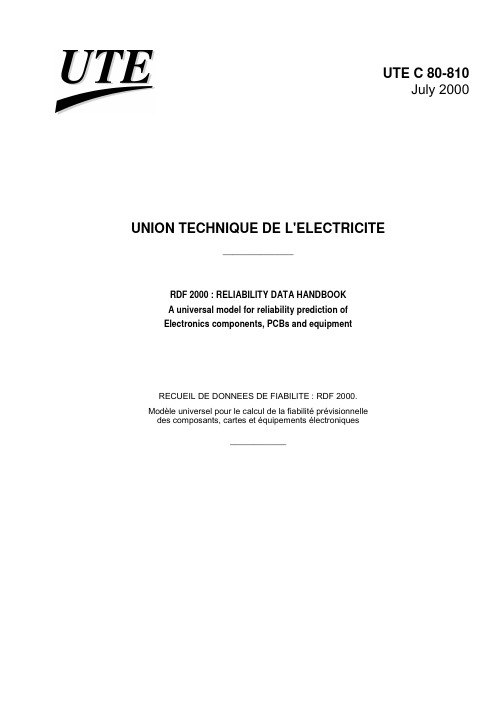
ISL6752(6754)EVAL1Z ZVS DC Power Supply with Synchronous Rectifiers User Guide
Application Note 1603Author: Richard GarciaISL6752/54EVAL1Z ZVS DC/DC Power Supply with Synchronous Rectifiers User GuideThe ISL6752/54EVAL1Z is a new design based on the ISL6752EVAL1Z but with several design modifications to improve the efficiency from 90% to 95%. The control circuit has been moved off the main board onto a daughter card. Two different daughter cards are provided: one using the ISL6752 and the other using the ISL6754. Both control cards utilize the Intersil zero voltage switching (ZVS) topology. The ISL6752 daughter card features pulse by pulse current limiting, and the ISL6754 daughter card features a patented method for average current limiting that results in a brick-wall current limit profile.The PCB layout of the ISL6752/54EVAL1Z has also been greatly improved over the ISL6752EVAL1Z. Even though the overall size of the board has been reduced, the copper losses have been reduced.In addition to the ZVS function, this board also incorporates N-Channel FETs as secondary side rectifiers, also known as synchronous rectifiers (SR). Power dissipation of the secondary side rectifiers is reduced because the conduction losses of SRs are significantly less than the conduction losses of PN or Schottky diodes.ScopeThis application note covers implementation of synchronous rectifiers (SRs) and their associated drive circuits as used on the ISL6752/54EVAL1Z board. Implementation of the primary side ZVS controller, based on the ISL6752 daughter card, is described extensively in Intersil Application Note AN1262, “Designing with the ISL6752, ISL6753 ZVS Full-Bridge Controllers.”Also reviewed is the performance of this evaluation board. Oscillographs illustrate the performance of the power supply with load transients on the output. The ZVS switching of the bridge FETs is shown, and efficiency and load regulation are measured.At the end of this application note, the schematics, bill of materials, and printed circuit board layouts are included for reference.TABLE 1.SPECIFICATIONSAbsolute Maximum Input Voltage450VDCOperating Input Voltage 350V to 450VDCMaximum Input Current 2.5ADC Rated Output Current50ADC Current Limit 60A ± 5%Output Voltage12V ± 5%Efficiency at 100% (50A) Load 95%Efficiency at 20% (10A) Load92%FIGURE 1.NEW ISL6752/54EVAL1ZBlock DiagramThe evaluation board is composed of several distinct circuit elements. The three main sections are the ZVS full bridge on the input, the current doubler rectifier on the output, and the controller daughter card. See “Schematics- Main Board,ISL6752/54EVAL1Z” on page23 and “Schematics - Daughter Card” on page25 for complete circuit details.Daughter CardsThe ISL6752 or ISL6754 control ICs are located on their respective daughter cards, as shown in Figures 3 and 4. Both daughter cards have the control ICs on the primary side and the voltage error amplifier on the secondary side. Creepage spacing between the primary and secondary is maintained on the cards. The ISL6752 and the ISL6754 control ICs are located on the primary side, eliminating the need for two AC line isolating gate drive transformers to drive the primary side bridge FETs. Instead, the low side FETs are driven directly by MOSFET drivers (on the main board), and the high side FETs are driven by a gate drive transformer that only requires operational insulation. Primary side control also simplifies design of the current sensing transformers because they also do not have to be AC line isolating.A line isolation rated opto-coupler (D5 on ISL6752DB or D2 on ISL6754DB) passes the analog error signal generated by the error amplifier, U1, from the secondary to the primary. Opto D3 passes a digital signal from primary to secondary to turn off the SRS for diode emulation. The only functional difference between the ISL6752 andISL6754 daughter cards is how current limit is implemented. The ISL6752 uses pulse-by-pulse current limit, and the ISL6754 uses average current limit.Special test points located on the daughter cards aid in probing nodes on the daughter cards for evaluation. Test points PGND and TP_PRI are located on the primary side, and SGND andTP_SEC are located on the secondary. With these test points, the user can employ the spring-like probe accessories included withFIGURE 2.ISL6752/54EVAL1Z BLOCK DIAGRAMFIGURE 3.ISL6752 DAUGHTER CARDmany scope probes. The scope signal pin is inserted in TP_PRI (or TP_SEC), and the short spring ground lead is inserted in PGND (or SGND).To probe any node on the daughter card, solder a 30ga insulated wire between the desired node and the via that is associated with the TP_PRI or TP_SEC test point. This method not only simplifies probing of any node, but also implements the preferredtechnique of measuring small signals in the presence of high amplitude switching magnetic fields.The ISL6752DBEVAL1Z and the ISL6754DBEVAL1Z daughter cards are also available as standalone evaluation kits.ZVS Full BridgeThe low side FETs, Q 3 and Q 4, are driven directly by the ISL89160 MOSFET driver, U1 (Figure 5). The two high-side FETs, Q 1 and Q 2, are indirectly driven by the ISL89160 driver, U2. A level translating gate drive transformer, T 3, with complementary output windings, directly drives the high-side bridge FETs with a symmetrical square wave. The design of T 3 is simplified because it only needs 400V operational insulation, and it is always driven with a square wave, thus eliminating the problems associated with non-symmetrical drive waveforms.Observe that the ISL89160 MOSFET drivers are located as close as possible to their respective bridge FETs to minimize thedetrimental effects of parasitic inductance on the outputs of the drivers. Although the input signal lead lengths between the drivers and the daughter card are relatively long (about 5cm), they are shielded on top and bottom by ground planes, to significantly reduce the noise injected on these lines. Thehysteresis of the ISL89160 inputs also lessens the possibility of noise corrupting the gate signals.High Voltage ProtectionBecause a failure of the bridge can cause catastrophic damage to the primary side control elements, a voltage crowbar, F1 and D 3, and a voltage blocking diode, D 4, are incorporated (Figure 6). D 3 clamps the bias voltage to a safe level. If 400V is applied to the V DD node, F1 opens shortly after D3 conducts current. D 4provides additional protection by blocking high voltage from being applied to the 13V lab supply. Note that a fully debugged power supply does not need these additional components. These parts are included on the evaluation board to minimize damage, should the user accidently introduce a fault while evaluating thecircuits. The designer may want to keep F1 in the final design, toprevent a loud bang if the bridge does fail.FIGURE 4.ISL6754 DAUGHTER CARDFIGURE 5.FULL BRIDGEFIGURE 6.PROTECTION CIRCUITSPrimary Side Current SensingThe primary side bridge has two current sensing transformers, T 2 and T 4, one on each leg on the drains of the low-side bridge FETs (Figure 7). Using two transformers allows each CT to reset during alternate half cycles. Alternate current sensing methods are reviewed in “Current Sensing” on page 8.Synchronous Rectifier Drive CircuitTwo banks of SRs are driven by the ISL89163 MOSFET driver, U4 (Figure 8). An RCD network on the inputs to this driver delay the turn-on of the SRs relative to the turn-off of the primary side bridge FETs.The ISL89367, U108, can optionally be used to drive the SRs instead of the ISL89163. Review “Schematics - Daughter Card” on page 25 to understand how to disconnect the ISL89163 and connect the ISL89367.The pulse transformer, T 6, crosses the isolation boundary to couple the control signals from the ISL6752, ISL6754 to the MOSFET drivers (Figure 9). Note that this transformer alsoprovides the secondary side bias voltage for the MOSFET drivers.Current Doubler OutputThe current doubler output is composed of two banks of SRs, Q 107... Q 109 and Q 111... Q 113; inductors L 102and L 103; and output filter capacitors, C 133... C 136 (Figure 10). The advantage of this topology is that the output current is shared by the two inductors, thus reducing conduction losses. Another advantage isthat the secondary winding of the power transformer does not require a center tap.FIGURE 7.PRIMARY SIDE CURRENT SENSINGFIGURE 8.SRs AND DRIVERSFIGURE 9.PULSE TRANSFORMER AND DRIVERBasic SR PrinciplesReplacing diodes with MOSFETs has two major advantages:•Dramatically reduces conduction losses•The applied duty cycle remains virtually constant from no load to full load. Disadvantages are:•Additional complexity and cost•Higher reverse recovery losses as compared to fast recovery diodes.•When paralleling units for redundancy, provisions must be made to prevent current circulation among the paralleled units.SR Drive Timing RequirementsTo emulate a diode, an SR must be driven ON when a diode would normally be conducting. But unlike a diode, if the SR is ON, the current through the SR can reverse if the voltage on the SR “cathode” becomes positive. The consequence is that if the SR is driven ON when the primary side is sourcing voltage to the secondary, the secondary side will be shorted by the SR. Figure 11 illustrates the timing required to drive the SRs. Notethat the rising edges of the two lower bridge FETs are delayed bythe ISL6752/54 relative to the PWM signal. Likewise, the risingedges of the SRs gate signals are delayed by the ISL89163relative to the falling edge of the PWM signal. These delays arenecessary to prevent the overlap of drive signals that wouldresult with high amplitude short circuit currents.When an SR is turned off while current is flowing from source todrain, the current diverts from the FET channel to the internalbody diode. Because the voltage drop across the body diode ishigher than the channel, it is desirable to minimize dissipation byminimizing the duration of the current flow through the bodydiode.FIGURE 10.CURRENT DOUBLER OUTPUTFIGURE 11.TIMING FOR SRs AND BRIDGE FETsSR Drive and BiasOUTLLN and OUTLRN in Figure 12 are control signals from the ISL6752/54 that are used to drive the SRs. Because theISL6752/54 is located on the primary side, a pulse transformer, T6, is used to cross the isolation boundary. The simplified schematic of Figure 12 illustrates the use of T6 to not only couple OUTLLN and OUTLRN to the secondary, but also to generate the bias for drivers on the secondary.When /OUTLLN or /OUTLRN (outputs of EL7212) transitions to a logic high, it is necessary to turn off the associated SR quickly. For example, when /OUTLRN (blue) transitions high, V1 is high, and C10 is quickly discharged by Q100. U4 then drives R-SR off. In a similar manner, when /OUTLLN is high, U4 drives L-SR off. When /OUTLLN or /OUTLRN transitions to a logic low, it is necessary to turn on the SRs after a time delay, to prevent the SRs from shorting the primary side bridge when it is sourcing current. For example, when /OUTLRN transitions to low, V1 is low and Q100 turns off, allowing C10 to be charged by R27. When the positive threshold of UR is exceeded, the output of U4 drives on R_SR. In a similar manner, the high to low transition of/OUTLLN results in the output of U4 driving on L_SR after a time delay.Note that the cathodes of D9 are connected together to peak charge C123. Because C123 is large in value, after the initial charging, the voltage does not change significantly from cycle to cycle. An important aspect of generating the bias for U4 in this manner is that the thresholds for the logic transitions on the inputs of U4 are proportional to VBIAS, and the voltage to charge C9 and C10 is also VBIAS. Consequently, the delays generated by the RC networks are independent of the absolute value of VBIAS. Current DoublerFigure 13 illustrates the current flow in the two inductors of the current doubler topology. Current flow in the circuit is correlated with the waveforms by color coding. The green waveform represents the sum of red and blue currents through R LOAD. For circuit clarity, paralleled SRs and output capacitors of theISL6752/54EVAL1Z board are not shown.When using diodes (instead of SRs), if the average load current is less than half of the ramp current in the output inductors, the current in the inductors becomes discontinuous, and the duty cycle of the PWM is shortened to maintain the desired output voltage. When using SRs, the inductor currents in L1 and L2 can become negative because current in SRs can flow bidirectionally; consequently, the duty cycle remains virtually unchanged. The benefit is that the load transient performance is the same for any load from zero up to current limit. Another advantage is that, for very light loads, the duty cycle is not reduced to very small duty cycles, pulse skipping does not occur, and the associated voltage jitter does not happen.An important design consideration for the current doubler topology is that the DC resistance of both halves must be equal. PCB layout must be as symmetrical as possible, and the DCRs of the inductors should be reasonably equal. If not, the current between the two sides does not split equally. Because perfect physical PCB symmetry is not always possible, current sharing between inductors must be confirmed.In Figure 14, inductor current waveforms are taken from the ISL6752/54EVAL1Z board. Current balance between the two inductors was achieved after one board revision. The inductor currents maintain the same waveform shape even at no load. Another design consideration when using SRs is how to connect the outputs of multiple power supplies in parallel for redundancy or increased power capacity. A consequence of negative current flow in an SR (when a diode would otherwise be reverse biased and off) is that power can be transferred from the secondary to the primary if one of the paralleled outputs has a higher voltage. The voltage loop of the units with lower set point voltages attempts to pull down the voltage by sinking current from the higher set point units. The primary side bridge capacitor is charged by the secondary side, eventually resulting in excessive voltage damage. This damage can be avoided by using OR-ing diodes (or FETs) on the paralleled outputs. Another solution is to turn off the SRs (diode emulation mode) when the current reverses in the SRs, but this eliminates some of the advantages of using SRs. Paralleling features are not implemented on the ISL6752/54EVAL1Z board.FIGURE 13.CURRENT FLOW IN TWO INDUCTORS OF CURRENT DOUBLER TOPOLOGYFIGURE 14.INDUCTOR CURRENT WAVEFORMS 50A LOAD30A LOAD NO LOADCurrent SensingCurrent flowing from the secondary to the primary can result in an unanticipated malfunction of the current sensing transformer circuit if reverse SR currents are not considered. Figure 15 shows a commonly used primary side current sensing circuit utilizing one current sensing transformer (CT).This circuit works well for peak current mode control if power is always flowing from primary to secondary, as is the case when diodes are used instead of SRs. Figure 16 illustrates the performance of the current sensing output when power always flows from primary to secondary.The voltage across R S is as expected. The vertical dashed lines show when the power cycle is terminated at the required peak of the current.Figure 17 illustrates what happens at no load to the sense voltage across R S.Notice that the negative components of the primary transformer current are rectified, resulting in two peaks of current across R S for each half cycle. Under steady state conditions, the rectified negative component may cause erratic performance because the cycle can terminate on the first peak (the inverted peak, as indicated by the vertical red line) instead of the required second peak. This condition can easily be corrected by having a small load across the output to ensure that the negative peak is always less than the positive.A minimum load, however, does not correct a more serious problem that occurs when there is a large load step from a heavy load to no load. When the load current is interrupted, the output capacitor charges higher than the regulated voltage. As the regulation loop is starting to respond by slewing to a minimum duty cycle, the excessive voltage on the output capacitor starts to discharge back to the primary. This results in a large negative current at the beginning of the duty cycle, which causes the duty cycle to be terminated very early. The imbalance of the applied volt-seconds to the power transformer may saturate the power transformer and damage the power bridge.Another scenario is that the current sensing transformer itself may saturate, which also damages the bridge. The control loop cannot maintain balanced alternate half cycles applied to the power transformer without valid current sense information. There are three solutions to this problem. Figure 18 illustrates the placements of two current sensing transformers, one on each drain leg of the bottom FETs.In this configuration, only positive current flowing into the drains of the bottom FETs are sensed across R S, solving the problem of rectified negative currents being impressed across R S. An advantage of using two CTs is that there is a full half cycle available to reset the cores of the CTs. This is the solution used in the ISL6752/54EVAL1Z board.FIGURE 15.PRIMARY SIDE CURRENT SENSING CIRCUIT UTILIZINGONE CTFIGURE 16.PERFORMANCE OF CURRENT SENSING OUTPUTFIGURE 17.NO LOAD SENSE VOLTAGE ACROSS R SFigure 19 shows a different current sensing implementation that also solves the problem shown in Figure 15. In this example, both drain currents of the bottom FETs are sensed by only one CT. There are some limitations that must be considered, however. The minimum time available to reset the core is the duration of the selected dead time between the two FETs on the same side of the bridge. To accommodate the resetting of the CT, this dead time can be made longer, but the consequences of reducing the maximum duty cycle available for output voltage regulation mustIf the dead time is kept short, then the peak voltage required for resetting the core is relatively large. For example, assume that the selected dead time is 2% of the duty cycle. The resultingworst-case reset voltage is shown approximately in Equation1:In Equation 1, V SMAX is 1V (the current limit voltage of theISL6752); this is the ideal reset voltage. In practice, however, the parasitic capacitance of the output windings suppresses the peak voltage, and consequently, the reset time increases. If a custom current sensing transformer is designed, the effects of the parasitic capacitance can be minimized by increasing the space between turns. If a standard, off-the-shelf transformer is used, however, the output capacitance may be too large to allow long duty cycles. In this case, the two-transformer solution may be necessary.Notice in Figure 19 that the 400V RTN is slightly more negative than signal ground. This configuration is recommended for applications that directly drive the bottom FETs with MOSFET drivers. If the 400V RTN and the MOSFET drivers are grounded, regenerative feedback will be present on the output of the MOSFET drivers because of the CT windings in the gate drive loop.A variation on the current sense circuit in Figure 19 is to place the current sensing transformer in the common drain lead of the two high-side FETs, as shown in Figure 20.The circuits shown in Figures 19 and 20 give exactly the same performance, but the problem associated with the gate drives (as explained in Figure 19) is avoided. The disadvantage of placing the CT at this location is that the CT must be designed with400VDC operational insulation.ConclusionThis application note reviews the use of MOSFETs as synchronous rectifiers to replace conventional diodes. The advantages of improved power efficiency and load transient are reviewed along with implementation problems that must be solved.The use of daughter cards for the ISL6752 and ISL6754 control ICs also allows comparison of cycle-by-cycle peak current limiting and average current limiting.TRANSFORMERSFIGURE 19.CURRENT SENSING TRANSFORMER IN THE COMMON SOURCE LEAD0.980.02⁄()V SMAX49V=•(EQ. 1)FIGURE 20.DRAIN LEADReferences[1]Fred Greenfeld, Intersil Application Note AN1246,“Techniques to Improve ZVS Full-bridge Performance”[2]Fred Greenfeld, Intersil Application Note AN1262, “Designingwith the ISL6752, ISL6753 ZVS Full-bridge Controllers”[3]Richard Garcia, Intersil Application Note AN1619, “Designingwith ISL6752DBEVAL1Z and ISL6754DBEVAL1Z ControlCards”Evaluation Board Set-upThe following sections cover the set-up of theISL6752/54EVAL1Z evaluation board. Also included are waveforms, performance parameters, PCB layout, and schematics.Setting UpLab Equipment Required•DC bias power supply, 12.6VDC @ 200mA minimum •Adjustable 0VDC-400VDC regulated lab power supply, 2.5ADC minimum with current limit•Fan to cool heatsinks•Oscilloscope, digital preferred, with 4 channels, 20MHz minimum bandwidth•Adjustable DC load (electronic or resistor), 70A @ 12V,100A @ 0V min, >850W•DC Multimeter•Infra-red temperature probe (optional but highly recommended)Turn-On Procedure1.Solder a wire between DISABLE and PGND-1 lugs located onthe lower left side of the main board. Optionally connect a switch between these two lugs.2.Install either of the daughter control cards onto the mainboard.3.Connect the DC load to the outputs of the evaluation board.Adjust the load to zero current.4.With both supplies turned off, connect the DC bias supply tothe +13V terminal and PGND.5.Connect the 400V supply to +400V and 400V RTN.6.Turn on the DC bias supply and adjust the current limit to200mA. Adjust the voltage to +12.6 VDC. The lab supplycurrent should be approximately 150mA.7.Turn on the 400V supply and adjust the current limit to 2.5A.Adjust the voltage to 400VDC. Do not exceed 450VDC. The current should be approximately 45mA.8.Turn on the fan and direct the air flow through the heatsinksmounted on the bottom of the board.ing the test points that are adjacent to the output powerlugs, measure the output voltage of 12V ±0.5VDC.The output load and input voltage can now be safely adjusted. Because there is no thermal shut-down circuit, it is important to maintain adequate airflow over the heatsinks, especially when applying large loads. It is recommended to measure the temperature of the power FETs (primary bridge and secondary SRs) to ensure that their temperatures do not exceed +85°C. It is usually necessary to have only a moderate airflow over the heatsinks, even under worst-case loads.Danger•This evaluation unit should be used and operated only by persons experienced and knowledgeable in the design and operation of high voltage power conversion equipment. •Use of this evaluation unit constitutes acceptance of all risk inherent in the operation of equipment having accessible hazardous voltage. Careless operation may result in serious injury or death.•Use safety glasses or other suitable eye protection.•A line isolated 400VDC supply is required. CautionA voltage clamp, D3, is used to protect the primary side control circuit from catastrophic damage should the high voltage bridge fail. In order to prevent this clamp from conducting, do not adjust the bias supply above 13.5VDC.WaveformsZVSIn Figure 21, the drain-source voltage of the low-side FETs relative to the gate voltage is displayed to highlight the ZVS performance of the bridge. The load is at the rated 50A. Notice that full ZVS is not achieved because the minimum resonance voltage is about 25VDC. Also, the gate drive is turning on late (about 25ns), allowing the resonant voltage to start rising. Eventhough the optimum zero voltage switching is not achieved, 98% of the switching losses are still recovered [(4002-502)/4002=98%]. This improvement over the ISL6752EVALZ was achieved by increasing the leakage inductance of thetransformer and by using bridge FETs with less body capacitance.In Figure 22, resonant switching with 50% load still saves 84% of the switching losses. Other techniques can be used to improve ZVS performance. For more information, see Application NoteAN1246, “Techniques to Improve ZVS Ful-bridge Performance”.ZVS WaveformsFIGURE 21.RESONANT SWITCHING WITH 100% (50A) LOADFIGURE 22.RESONANT SWITCHING WITH 50% (25A) LOADLoad Transients WaveformsFIGURE 23.STEP LOAD: 0A TO 12.5A (12.5A DELTA)FIGURE 24.STEP LOAD: 25A TO 37.5A (12.5A DELTA)FIGURE 25.STEP LOAD: 37.5A TO 50AFIGURE 26.STEP LOAD: 0A TO 25AFIGURE 27.STEP LOAD: 0A TO 50AFIGURE 28.SHORT CIRCUIT RELEASE WITH ISL6754V OUT recovers after a short circuit is removed when using the ISL6754DBEVAL controller.After the short is removed, V OUT increases linearly because the output capacitance is being charged with a constant current (~55A).NOTE:Output Ripple and Noise WaveformsFIGURE 29.OUTPUT RIPPLE, 50A LOAD, 40MHz BANDWIDTHFIGURE 30.OUTPUT RIPPLE, 50A LOAD, 145MHz BANDWIDTHTransformer Current, Primary Winding WaveformsFIGURE 31.PRIMARY TRANSFORMER CURRENT vs OUTPUT LOAD TRANSIENT (25A TO 50A)FIGURE 32.PRIMARY TRANSFORMER CURRENT vs OUTPUT LOAD TRANSIENT (50A TO 25A)Performance CurvesFIGURE 33.POWER EFFICIENCY vs LOAD (ISL6752 OR ISL6754)FIGURE 34.LOAD REGULATION FIGURE 35.PULSE BY PULSE vs AVERAGE CURRENT LIMIT21015202570758085909295100OUTPUT CURRENT (A)E F F I C I E N C Y (%)6560555030354045505592% EFFICIENCY WITH 20% LOAD12.0011.9511.9011.8511.80ISL6754ISL6752102030405060I OUT (A)V O U T (V )01020304050607080I OUT (A)V O U T (V )121086420ISL6754ISL6752Application Note 1603Bill of MaterialsPART NUMBERQTY UNITS REFERENCE DESIGNATORDESCRIPTION MANUFACTURER MANUFACTURER PART ISL6752/54EVAL1ZREVBPCB1eaPWB-PCB,ISL6752_54EVAL1Z, REV B, ROHSIMAGINEERING INCISL6752/54EVAL1ZREVBPC BC3216X7R1C475K-T 2eaC11, C17CAPACITOR, SMD, 1206, 4.7µF, 16V, 10%, X7R, ROHSTDK C3216X7R1C475KC4532X7R2J104K-T 2ea C5, C18CAP, SMD, 1812, 0.1µF, 630V, 10%, X7R, ROHSTDKC4532X7R2J104K GA355QR7GF332KW01L-T 2ea C20, C121CAP, SMD, 2220, 3300pF, 250V, 10%, X7R, ROHSMURATA GA355QR7GF332KW01L H1046-00102-100V10-T 2ea C14, C15CAP, SMD, 0805, 1000pF, 100V, 10%, X7R, ROHSVENKEL C0805X7R101-102KNE H1046-00102-50V5-T 2ea C9, C10CAP, SMD, 0805, 1000pF, 50V, 5%, NP0, ROHS PANASONIC ECU-V1H102JCX H1046-00105-25V10-T 5ea C6, C12, C13, C16, C22CAP, SMD, 0805, 1.0µF, 25V, 10%, X5R, ROHS AVX 08053C105KAT2A H1065-00106-25V10-T 1ea C123, C132CAP, SMD, 1206, 10µF, 25V, 10%, X5R, ROHS VENKEL C1206X5R250-106KNE H1082-00475-50V10-T 4ea C7, C8, C127, C129CAP, SMD, 1210, 4.7µF, 50V, 10%, X7R, ROHS MURATA GRM32ER71H475KA88L SER2814L-332KL2eaL102, L103COIL-PWR INDUCTOR, SMD, 3.3µH, 10%, 48A, 1.2m Ω, ROHS COILCRAFTSER2814L-332KLUUG1C222MNL1ZD 4ea C133-C136CAP, SMD, 16X16.5, 2200µF, 16V, 20%, AL.EL., ROHS NICHICON UUG1C222MNL1ZDUUG2W330MNL1MS 4ea C1-C4CAP, SMD, 18X21.5, 33µF, 450V, 20%, ALUM.ELEC, ROHS NICHICON UUG2W330MNL1MS131-4353-001ea VOUT CONN-SCOPE PROBE TEST PT, COMPACT, PCBMNT, ROHSTEKTRONIX 131-4353-001514-26eaa) 13VDC, 400VDC, PGND-1, PGND-2, DISABLE CONN-TURRET, TERMINAL POST, TH, ROHSKEYSTONE 1514-21514-20ea b) 400VDC_RTNCONN-TURRET, TERMINAL POST, TH, ROHSKEYSTONE 1514-250029ea a) CS+, VREF, OUTLL, OUTLR, OUTUL, OUTUR CONN-MINI TEST POINT, VERTICAL, WHITE, ROHS KEYSTONE500250020ea b) SR_EN, OUTLLN, OUTLRNCONN-MINI TEST POINT, VERTICAL, WHITE, ROHSKEYSTONE 50025016-T13eaa) GLL, GLR, LLN, LRN, SR_A, SR_B, PGND-3, 2, +12VOUT, 12V RTN CONN-COMPACT TEST POINT, SMD, ROHS KEYSTONE50165016-T 0ea b) SGND-1, SGND-CONN-COMPACT TEST POINT, SMD, ROHSKEYSTONE 50165016-Teac) L_PHASE, R_PHASE CONN-COMPACT TESTPOINT, SMD, ROHSKEYSTONE5016。
opto-couplers
2.0 TJ = 25°C 1.8
1.6 1.4
1.2 1.0 1.0
2.0
5.0 10 20 50 100 200 IF, Instantaneous Forward Current (mA)
500 1000
COUPLER CHARACTERISTICS
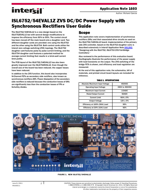
The 4N25 is an optical coupler consisting of a gallium arsenide (GaAs) LED and a silicon phototransistor. (For more information on LEDs and phototransistors, see References 1 and 2.) The coupler's characteristics are given in the following sequence: LED characteristics, phototransistor characteristics, coupled characteristics, and switching characteristics. Table 1 shows all four for the 4N25 series.
Characteristic *Reverse Leakage Current (VR = 3.0 V, RL = 1.0 M ohms) *Forward Voltage (IF = 50 mA) Capacitance (VR = 0 V, f = 1.0 MHz) Characteristic *Collector–Emitter Dark Current (VCE = 10 V, Base Open) *Collector–Base Dark Current (VCB = 10 V, Emitter Open) *Collector–Base Breakdown Voltage (IC = 100 A, IE = 0) *Collector–Emitter Breakdown Voltage (IC = 1.0 mA, IB = 0) *Emitter–Collector Breakdown Voltage (IE = 100 A, IB = 0) DC Current Gain (VCE = 5.0 V, IC = 500 A) 4N25, 4N26, 4N27 4N28 Symbol IR VF C Min — — — Typ 0.05 1.2 150 Max 100 1.5 — Unit A Volts pF
Proteus所有元件名称
元件名称中文名说明RESPACK-8 排阻7407 驱动门1N914 二极管74Ls00 与非门74LS04 非门74LS08 与门74LS390 TTL 双十进制计数器7SEG 4针BCD-LED 输出从0-9 对应于4根线的BCD码7SEG 3-8译码器电路BCD-7SEG[size=+0]转换电路ALTERNATOR 交流发电机AMMETER-MILLI mA安培计AND 与门BATTERY 电池/电池组BUS 总线CAP 电容CAPACITOR 电容器CLOCK 时钟信号源CRYSTAL 晶振D-FLIPFLOP D触发器FUSE 保险丝GROUND 地LAMP 灯LED-RED 红色发光二极管LM016L 2行16列液晶可显示2行16列英文字符,有8位数据总线D0-D7,RS,R/W,EN三个控制端口(共14线),工作电压为5V。
没背光,和常用的1602B功能和引脚一样(除了调背光的二个线脚)LOGIC ANALYSER 逻辑分析器LOGICPROBE 逻辑探针LOGICPROBE[BIG] 逻辑探针用来显示连接位置的逻辑状态LOGICSTATE 逻辑状态用鼠标点击,可改变该方框连接位置的逻辑状态LOGICTOGGLE 逻辑触发MASTERSWITCH 按钮手动闭合,立即自动打开MOTOR 马达OR 或门POT-LIN 三引线可变电阻器POWER 电源RES 电阻RESISTOR 电阻器SWITCH 按钮手动按一下一个状态SWITCH-SPDT 二选通一按钮VOLTMETER 伏特计VOLTMETER-MILLI mV伏特计VTERM 串行口终端Electromechanical 电机Inductors 变压器Laplace Primitives 拉普拉斯变换Memory IcsMicroprocessor IcsMiscellaneous 各种器件AERIAL-天线;ATAHDD;ATMEGA64;BATTERY;CELL;CRYSTAL-晶振;FUSE;METER-仪表;Modelling Primitives 各种仿真器件是典型的基本元器模拟,不表示具体型号,只用于仿真,没有PCBOptoelectronics 各种发光器件发光二极管,LED,液晶等等PLDs & FPGAsResistors 各种电阻Simulator Primitives 常用的器件Speakers & SoundersSwitches & Relays 开关,继电器,键盘Switching Devices 晶阊管Transistors 晶体管(三极管,场效应管)TTL 74 seriesTTL 74ALS seriesTTL 74AS seriesTTL 74F seriesTTL 74HC seriesTTL 74HCT seriesTTL 74LS seriesTTL 74S seriesAnalog Ics 模拟电路集成芯片Capacitors 电容集合CMOS 4000 seriesConnectors 排座,排插Data Converters ADC,DACDebugging Tools 调试工具ECL 10000 Series------------------------------------------------------------PROTEUS元件库元件名称及中英对照AND 与门ANTENNA 天线BATTERY 直流电源BELL 铃,钟BVC 同轴电缆接插件BRIDEG 1 整流桥(二极管)BRIDEG 2 整流桥(集成块) BUFFER 缓冲器BUZZER 蜂鸣器CAP 电容CAPACITOR 电容CAPACITOR POL 有极性电容CAPVAR 可调电容CIRCUIT BREAKER 熔断丝COAX 同轴电缆CON 插口CRYSTAL 晶体整荡器DB 并行插口DIODE 二极管DIODE SCHOTTKY 稳压二极管DIODE VARACTOR 变容二极管DPY_3-SEG 3段LEDDPY_7-SEG 7段LEDDPY_7-SEG_DP 7段LED(带小数点) ELECTRO 电解电容FUSE 熔断器INDUCTOR 电感INDUCTOR IRON 带铁芯电感INDUCTOR3 可调电感JFET N N沟道场效应管JFET P P沟道场效应管LAMP 灯泡LAMP NEDN 起辉器LED 发光二极管METER 仪表MICROPHONE 麦克风MOSFET MOS管MOTOR AC 交流电机MOTOR SERVO 伺服电机NAND 与非门NOR 或非门NOT 非门NPN NPN三极管NPN-PHOTO 感光三极管OPAMP 运放OR 或门PHOTO 感光二极管PNP 三极管NPN DAR NPN三极管PNP DAR PNP三极管POT 滑线变阻器PELAY-DPDT 双刀双掷继电器RES1.2 电阻RES3.4 可变电阻RESISTOR BRIDGE ? 桥式电阻RESPACK ? 电阻SCR 晶闸管PLUG ? 插头PLUG AC FEMALE 三相交流插头SOCKET ? 插座SOURCE CURRENT 电流源SOURCE VOLTAGE 电压源SPEAKER 扬声器SW ? 开关SW-DPDY ? 双刀双掷开关SW-SPST ? 单刀单掷开关SW-PB 按钮THERMISTOR 电热调节器TRANS1 变压器TRANS2 可调变压器TRIAC ? 三端双向可控硅TRIODE ? 三极真空管VARISTOR 变阻器ZENER ? 齐纳二极管DPY_7-SEG_DP 数码管SW-PB 开关----------------------------------------------------------------------PROTEUS原理图元器件库详细说明Device.lib 包括电阻、电容、二极管、三极管和PCB的连接器符号ACTIVE.LIB 包括虚拟仪器和有源器件DIODE.LIB 包括二极管和整流桥DISPLAY.LIB 包括LCD、LEDBIPOLAR.LIB 包括三极管FET.LIB 包括场效应管ASIMMDLS.LIB 包括模拟元器件VALVES .LIB 包括电子管ANALOG.LIB 包括电源调节器、运放和数据采样IC CAPACITORS.LIB 包括电容COMS.LIB 包括4000系列ECL.LIB 包括ECL10000系列MICRO.LIB 包括通用微处理器OPAMP.LIB 包括运算放大器RESISTORS.LIB 包括电阻FAIRCHLD .LIB 包括FAIRCHLD 半导体公司的分立器件LINTEC.LIB 包括LINTEC公司的运算放大器NATDAC.LIB 包括国家半导体公司的数字采样器件NATOA.LIB 包括国家半导体公司的运算放大器TECOOR.LIB 包括TECOOR公司的SCR 和TRIAC TEXOAC.LIB 包括德州仪器公司的运算放大器和比较器ZETEX .LIB 包括ZETEX 公司的分立器件[分享]protues元器件查找代码7407 驱动门1N914 二极管74Ls00 与非门74LS04 非门74LS08 与门74LS390 TTL 双十进制计数器7SEG 4针BCD-LED 输出从0-9 对应于4根线的BCD码7SEG 3-8译码器电路BCD-7SEG转换电路ALTERNATOR 交流发电机AMMETER-MILLI mA安培计AND 与门BATTERY 电池/电池组BUS 总线CAP 电容CAPACITOR 电容器CLOCK 时钟信号源CRYSTAL 晶振D-FLIPFLOP D触发器FUSE 保险丝GROUND 地LAMP 灯LED-RED 红色发光二极管LM016L 2行16列液晶可显示2行16列英文字符,有8位数据总线D0-D7,RS,R/W,EN三个控制端口(共14线),工作电压为5V。
欧特顿产品9PX1500IRT2U-L入手指南说明书
Eaton 9PX1500IRT2U-LUPS Eaton 9PX, lithium, 1500 VA, 1500 W, entrée : C14, sorties :(8) C13, rack/tour, 2USpécifications généralesNom du produit Numéro de catalogueAlimentation sans interruption Eaton 9PX9PX1500IRT2U-LUPC Longueur du produit743172105479450 mmHauteur du produit Largeur du produit86.5 mm440 mmPoids du produit Conformité15.8 kg Marquage CECode de modèleEaton 9PX 1500i RT2U Li-IonLithium-ionVisualiser la courbe d’autonomie batterieBatteries internes et modules de batterie étendus (EBM) remplaçables à chaudOui (8) C13230 V1 500 W1200/208/220/230/240 V +/- 1% Onde sinusoïdale230V défaut (200/208/220/230/240V) 31Online/Double conversion1 500 VAC14230V défaut (200/208/220/230/240V)50/60 Hz>0,99176 -276 V (100-276 V avec déclassement)NonType de BatterieGraphe d'autonomie Remplacement de la batterie Gestion des batteriesAutonomie prolongée de la batterie PriseTensionPuissanceFacteur de puissance de sortiePlage de tension de sortieForme du signal de sortieTension de sortie nominaleDistorsion de tension à la sortie (charge linéaire) - max Type d’alimentationTopologiePuissance en VAConnexion d'entréeTension nominale d’entréeFréquence nominaleFacteur de puissance d’entrée Plage de la tension d'entrée Inclut la carte réseau Communication par bus de terrainBatteries lithium-ion avecsystème de gestion de labatteriereconnaissanceautomatique des modulesbatteries externes (EBM)Port USB (compatible HID)Port Série (RS232)Mini-bornier pour la fonctionmarche-arrêt à distanceMini-bornier pour la misehors tension à distanceMini-bornier pour relais desortieContacts secs (3 sorties,40-70 HzNonAfficheur à cristaux liquides graphique multilingue OuiUn emplacement pour carte de communication en option Eaton Intelligent Power Manager (IPM), Eaton Intelligent Power Protector (IPP)Autre3000 m <35 dB à 1 mètre 0° à 40°C (32° à 104°F)0-96 % sans condensationDispositif de 482,6 mm (19 pouces)1OuiPlage de fréquence d'entrée Interface Ethernet Interface utilisateurContact libre de potentiel Emplacement carte d’extensionCompatibilité logicielleType d'interface Altitude Niveau de bruit Plage de température Humidité relativeType de constructionContenu du colis Phase (sortie)Bypass interne une entrée, par optocoupleur, DB9)Alimentation sans interruption (ASI - UPS en anglais)(2) câbles de sortie IEC-IEC Câble USB Câble série(2) supports pour montage 19(2) Kit de montage en rack (2) supports pour montage tourSystème de verrouillage de câbleConsignes de sécuritéGuide de démarrage rapideEaton Corporation plc Eaton House30 Pembroke Road Dublin 4, Ireland © 2023 Eaton. Tous droits réservés.Eaton is a registered trademark.All other trademarks are property of their respective owners./socialmediaOui Noir/argent 92,5Oui1NonOnduleurs Eaton 9PX Lithium-ion 1500 VA - 3000 VA Eaton 9PX Lithium-Ion Advanced Users Guide Eaton 9PX Lithium-Ion UPS Quick Start GuideFonction arrêt automatique Couleur EfficacitéKit de montage rack Phase (entrée)Module de puissance débrochable sous tension Fiches techniquesGuide utilisateur。
MX-E 系列机器视觉处理器快速参考指南说明书
MX-E Processor with PNP (sourcing) I/OQUICK REFERENCE GUIDEDESCRIPTIONThis guide covers MX-E processor models that contain the letter “P.” For example MX-E20-2-P-1. These models provide PNP (sourcing) inputs and outputs.The MX-E series machine vision processors offer the most powerful and flexible way to solve even complex machine vision applications. • Rugged IP20 housing • Low Maintenance• 16 Inputs and Outputs • Up to 4 GigE cameras• Easily Accessed connectorsSYSTEM SPECIFICATIONSProcessorsMX-E20: Intel Celeron 1.4 GHz; MX-E40: Intel Celeron 2.2 GHz ; MX-E80: Intel Core i7 2.3 GHz StorageMX-E20 and MX-E40: 4 GB RAM - 60 GB SSD; MX-E80: 8 GB RAM - 128 GB SSDGigE camera portsMX-E20: 2; MX-E40 and MX-E80: 2 or 4All MX-E processors have the following specifications: • HD graphics (1920x1200)• 2 x 10/100/1000 Mbps Base-T Network Interface• Ethernet/IP, Modbus TCP, OPC communications are supported • 1 x RS232 port• 16 x Optically Isolated Digital In + 16 x Optically Isolated Digital Out • Microsoft Windows OEM Embedded Standard 7 64-bitSUPPLY VOLTAGE CONNECTIONPower Connector + 24VDC Supply Plus GND Functional Ground* - 24VDC Supply Minus*Connect to ground using a conductor with minimum 2.5 mm² cross-sectionSTATUS LEDS AND BUTTONS1. Power, green2. HDD, Yellow3. Link, Yellow4. Run, Green5.Power Button 6.Reset ButtonBehind Front CoverPower Button: Press and release to turn on the unit or shut down the OS and switch off the unit. Press and hold to switch off without OS shutdown. Reset Button: Triggers a hardware and PCI reset. The unit is restarted.HASP KEY USB PORT1. Reset Button2. USB Port for Hasp KeyTo enable cameras and licenses, insert the provided Hasp key in the USB port (labeled CONNECTORS1. USB 3.02. Ethernet 23. Ethernet 14. RS232 (COM 1)5. Display Port6. DVI for Monitor7. Supply Voltage8. 37 pin D-Sub Digital I/O9. M-Series or E-Series Camera(CAM1-CAM4) Cable 606-0677-xx 10. USB 2.0 – Keyboard/MouseDisplay PortTop ViewDIGITAL I/O CABLES TERMINALS AND CONNECTIONSCablePart Number Digital I/O 37-pin to Terminal Block 248-0110 606-0675-xx Digital I/O 37-pin to pigtail (remove one end)606-0675-xxBlue/BlackFemale ConnectorDIGITAL I/O SPECIFICATIONSCOMMUNICATIONSCamera communication uses Cat6 Ethernet cable and provides POE for M1xx and E1xx cameras. Use only Datalogic provided cables.I/O CONFIGURATIONVision Program Manager (VPM) software installed on the processor is used to create vision programs and configure input and output response. Refer to the Impact Reference Guide for programming details.MECHANICAL DIMENSIONSCAMERA CABLES, TERMINALS, AND CONFIGURATIONCamera trigger and strobe output are provided by an external 6-pin I/O cable with no connection to the processor. Use cable 606-0672-xx (unterminated) orEXAMPLE I/O CIRCUIT DIAGRAMSTECHNICAL DATASupply voltage (Vs) 24 VDC ± 25% Nominal Current Draw 5.5 A at 24 VDC Inputs16 opto-isolated Input currentON: 2.0 mA or more Off: 0.16 mA or lessOutputs16 opto-isolated current sinkingOutput Voltage 35 VDC (max)Output current100 mA max per outputOutput saturation voltage < 1 VNetwork interface 10/100/1000 Mbps Ethernet x 2 Camera interface GigE (x 2 or 4 depending on model)Dimensions 130 × 270 × 254.75 mm Data retention Non-volatile SSD memory TemperatureOperating: 0 °C to 55 °C Storage: -20 °C to 60 °C Relative Humidity (30 °C) Operating: 10 to 90% Storage: 5 to 95%Vibrations(EN60068-2-6) 2 to 8 Hz: 1.75 mm amplitude /9 to 200 Hz: 0.5 gShock resistance (EN60068-2-27) 11 MS (15 G) Housing materialGalvanized plate, plasticMechanical protection (EN 60529) IP20 Weight2050 gCOMPLIANCEOnly connect Ethernet and dataport connections to a network which has routing only within the plant or building and no routing outside the plant or building. CE COMPLIANCEWarning: This is a Class A product. In a domestic environment this product may cause radio interference in which case the user may be required to take adequate measures. FCC COMPLIANCEModifications or changes to this equipment without the expressed written approval of Datalogic could void the authority to use the equipment.This device complies with PART 15 of the FCC Rules. Operation is subject to the following two conditions: (1) This device may not cause harmful interference, and (2) this device must accept any interference received, including interference which may cause undesired operation.This equipment has been tested and found to comply with the limits for a Class A digital device, pursuant to part 15 of the FCC Rules. These limits are designed to provide reasonable protection against harmful interference when the equipment is operated in a commercial environment. This equipment generates, uses, and can radiate radio frequency energy and, if not installed and used in accordance with the instruction manual, may cause harmful interference to radio communications. Operation of this equipment in a residential area is likely to cause harmful interference in which case the user will be required to correct the interference at his own expense. DECLARATION OF CONFORMITYWe DATALOGIC AUTOMATION declare under our sole responsibility that these products are conform to the 2004/108/CE and successive amendments.WARRANTY DATALOGIC AUTOMATION warrants its products to be free from defects.DATALOGIC AUTOMATION will repair or replace, free of charge, any product found to be defective during the warranty period of 24 months from the manufacturing date.This warranty does not cover damage or liability deriving from the improper application of DATALOGIC AUTOMATION products.DATALOGIC AUTOMATIONVia Lavino 265 - 40050 Monte S.Pietro - Bologna – Italy Tel: +39 051 6765611 - Fax: +39 051 6759324e-mail:********************************DATALOGIC AUTOMATION cares for the environment: 100% recycled paper.DATALOGIC AUTOMATION reserves the right to make modifications and improvements without prior notification.Datalogic and the Datalogic logo are registered trademarks of Datalogic S.p.A. in many countries,including the U.S.A. and the E.U.821004221 (Rev A) © Copyright Datalogic 2016Inputs SpecificationFormat Opto-coupler isolated input Resistance 4.7k ΩOn current 2.0 mA or more Off current0.16 mA or less Response Time Within 200 µsecOutputs SpecificationFormatOpto-coupler isolated open collector output Output voltage 35 VDC (max)Output current 100mA (per channel max)Residual voltage output on0.5V or less (Output current≤50mA), 1.0V or less (Output current≤100mA) Response TimeWithin 200 µsecPower 24 VDCMM-+Supplied Power PlugInput Connection (Sourcing)Output Connection (Sourcing)MX-E Processor with NPN (sinking) I/OQUICK REFERENCE GUIDEDESCRIPTIONThis guide covers MX-E processor models that contain the letter “N.” For example MX-E20-2-N-1. These models provide NPN (sinking) inputs and outputs.The MX-E Series machine vision processors offer the most powerful and flexible way to solve even complex machine vision applications. • Rugged IP20 housing • Low Maintenance • 16 Inputs and Outputs • Up to 4 GigE cameras• Easily Accessed connectorsSYSTEM SPECIFICATIONSProcessorsMX-E20: Intel Celeron 1.4 GHz; MX-E40: Intel Celeron 2.2 GHz ; MX-E80: Intel Core i7 2.3 GHz StorageMX-E20 and MX-E40: 4 GB RAM - 60 GB SSD; MX-E80: 8 GB RAM - 128 GB SSDGigE camera portsMX-E20: 2; MX-E40 and MX-E80: 2 or 4All MX-E processors have the following specifications: • HD graphics (1920x1200)• 2 x 10/100/1000 Mbps Base-T Network Interface• Ethernet/IP, Modbus TCP, OPC communications are supported • 1 x RS232 port• 16 x Optically Isolated Digital In + 16 x Optically Isolated Digital Out • Microsoft Windows OEM Embedded Standard 7 64-bitSUPPLY VOLTAGE CONNECTIONPower Connector + 24VDC Supply Plus GND Functional Ground* - 24VDC Supply Minus*Connect to ground using a conductor with minimum 2.5 mm² cross-sectionSTATUS LEDS AND BUTTONS1. Power, green2. HDD, Yellow3. Link, Yellow4. Run, Green5.Power Button 6.Reset ButtonBehind Front CoverPower Button: Press and release to turn on the unit or shut down the OS and switch off the unit. Press and hold to switch off without OS shutdown. Reset Button: Triggers a hardware and PCI reset. The unit is restarted.HASP KEY USB PORT1. Reset Button2. USB Port for Hasp KeyTo enable cameras and licenses, insert the provided Hasp key in the USB port (labeled CONNECTORS1. USB 3.02. Ethernet 23. Ethernet 14. RS232 (COM 1)5. Display Port6. DVI for Monitor7. Supply Voltage8. 37 pin D-Sub Digital I/O9. M-Series or E-Series Camera(CAM1-CAM4) Cable 606-0677-xx 10. USB 2.0 – Keyboard/MouseDisplay PortTop ViewDIGITAL I/O CABLES TERMINALS AND CONNECTIONSCablePart Number Digital I/O 37-pin to Terminal Block 248-0110 606-0675-xx Digital I/O 37-pin to pigtail (remove one end)606-0675-xxBlue/BlackFemale ConnectorDIGITAL I/O SPECIFICATIONSCOMMUNICATIONSCamera communication uses Cat6 Ethernet cable and provides POE for M1xx and E1xx cameras. Use only Datalogic provided cables.I/O CONFIGURATIONVision Program Manager (VPM) software installed on the processor is used to create vision programs and configure input and output response. Refer to the Impact Reference Guide for programming details.MECHANICAL DIMENSIONSCAMERA CABLES, TERMINALS, AND CONFIGURATIONCamera trigger and strobe output are provided by an external 6-pin I/O cable with no connection to the processor. Use cable 606-0672-xx (unterminated) or EXAMPLE I/O CIRCUIT DIAGRAMSTECHNICAL DATASupply voltage (Vs) 24 VDC ± 25% Nominal Current Draw 5.5 A at 24 VDC Inputs16 opto-isolated Input currentON: 2.0 mA or more Off: 0.16 mA or lessOutputs16 opto-isolated current sinkingOutput Voltage 35 VDC (max)Output current100 mA max per outputOutput saturation voltage < 1 VNetwork interface 10/100/1000 Mbps Ethernet x 2 Camera interface GigE (x 2 or 4 depending on model)Dimensions 130 × 270 × 254.75 mm Data retention Non-volatile SSD memory TemperatureOperating: 0 °C to 55 °C Storage: -20 °C to 60 °C Relative Humidity (30 °C) Operating: 10 to 90% Storage: 5 to 95%Vibrations(EN60068-2-6) 2 to 8 Hz: 1.75 mm amplitude /9 to 200 Hz: 0.5 gShock resistance (EN60068-2-27) 11 MS (15 G) Housing materialGalvanized plate, plasticMechanical protection (EN 60529) IP20 Weight2050 gCOMPLIANCEOnly connect Ethernet and dataport connections to a network which has routing only within the plant or building and no routing outside the plant or building. CE COMPLIANCEWarning: This is a Class A product. In a domestic environment this product may cause radio interference in which case the user may be required to take adequate measures. FCC COMPLIANCEModifications or changes to this equipment without the expressed written approval of Datalogic could void the authority to use the equipment.This device complies with PART 15 of the FCC Rules. Operation is subject to the following two conditions: (1) This device may not cause harmful interference, and (2) this device must accept any interference received, including interference which may cause undesired operation.This equipment has been tested and found to comply with the limits for a Class A digital device, pursuant to part 15 of the FCC Rules. These limits are designed to provide reasonable protection against harmful interference when the equipment is operated in a commercial environment. This equipment generates, uses, and can radiate radio frequency energy and, if not installed and used in accordance with the instruction manual, may cause harmful interference to radio communications. Operation of this equipment in a residential area is likely to cause harmful interference in which case the user will be required to correct the interference at his own expense. DECLARATION OF CONFORMITYWe DATALOGIC AUTOMATION declare under our sole responsibility that these products are conform to the 2004/108/CE and successive amendments.WARRANTY DATALOGIC AUTOMATION warrants its products to be free from defects.DATALOGIC AUTOMATION will repair or replace, free of charge, any product found to be defective during the warranty period of 24 months from the manufacturing date.This warranty does not cover damage or liability deriving from the improper application of DATALOGIC AUTOMATION products.DATALOGIC AUTOMATIONVia Lavino 265 - 40050 Monte S.Pietro - Bologna – Italy Tel: +39 051 6765611 - Fax: +39 051 6759324e-mail:********************************DATALOGIC AUTOMATION cares for the environment: 100% recycled paper.DATALOGIC AUTOMATION reserves the right to make modifications and improvements without prior notification. Datalogic and the Datalogic logo are registered trademarks of Datalogic S.p.A. in many countries,including the U.S.A. and the E.U.821004221 (Rev A) © Copyright Datalogic 2016Inputs SpecificationFormat Opto-coupler isolated input Resistance 4.7k ΩOn current 2.0 mA or more Off current0.16 mA or less Response Time Within 200 µsecOutputs SpecificationFormatOpto-coupler isolated open collector output Output voltage 35 VDC (max)Output current 100mA (per channel max)Residual voltage output on0.5V or less (Output current≤50mA), 1.0V or less (Output current≤100mA) Response TimeWithin 200 µsecPower 24 VDCMMInput Connection (Sinking)Output Connection (Sinking) -+Supplied Power Plug。
PLC检测柴油机转速的设计
PLC检测柴油机转速的设计王蔚鸿;戚连锁;高申德【摘要】早期采用PLC设计柴油机的安全保护回路时,直接采用三线制转速传感器的脉冲信号经过处理后输出;后来应船级社要求,转速传感器回路需要增加断线检测功能,于是使用PLC配合光耦板来检测三线制转速传感器的回路是否正常并采集转速信号,但在应用中发现存在应急启动柴油机后没有运行信号的漏洞;最后研发了采用PLC、两线制转速传感器以及断线监测模块这三者配合起来检测转速传感器的回路是否正常并完成柴油机转速信号采集的功能。
每一次在功能上都有升级,但升级的同时也会带来其他问题,针对实际使用时出现的问题进行分析、研究,并提出一种新的解决方案。
%Early stage,when used PLC to design the diesel engine safety protection circuit,it used the three-wire signal of speed sensor directly and made some treatment,then outputted. Later,to satisfy the requirement of the classification society,the speed sensor safety protection circuit should own the disconnection detection function, so used PLC and optocouple plate to detect if the three-wire speed sensor circuit is normal and collect the speed signal,but ofter putted into use,it existed the loop hole that there was no operation signal when the diesel started in emergency mode. Finally, developed a method combine PLC,two-wire speed sensor and wire break supervision module the three partto detect if the speed sensor safety protection circuit was normal as well as collect the engine speed signal. Every time the detection method change could make the promotion of function, but the promotion also broughtother problems, this essay aims at the problem occurred in actual usage,makes analyzation and research,and presents a new solution.【期刊名称】《机电工程技术》【年(卷),期】2015(000)002【总页数】3页(P25-27)【关键词】可编程控制器;转速传感器;安全保护回路;断线检测【作者】王蔚鸿;戚连锁;高申德【作者单位】海军工程大学电气工程学院,湖北武汉 430000; 安庆中船柴油机有限公司,安徽安庆 246003;海军工程大学电气工程学院,湖北武汉 430000;安庆中船柴油机有限公司,安徽安庆 246003【正文语种】中文【中图分类】TM571.6+1DOI:10.3969/j.issn.1009-9492.2015.02.008在柴油机安保控制系统中,有一个非常重要的控制回路就是对柴油机的转速监控,自从继电器控制改为PLC控制后,柴油机转速检测回路经历了三个阶段,每一阶段都有一定的优点,但是也会带来一些其他的问题,正因为如此,需要在实际工作中不断思考、试验、完善设计工作,提出新的解决问题方案,提高产品的可靠性、降低成本,实现利润最大化。
- 1、下载文档前请自行甄别文档内容的完整性,平台不提供额外的编辑、内容补充、找答案等附加服务。
- 2、"仅部分预览"的文档,不可在线预览部分如存在完整性等问题,可反馈申请退款(可完整预览的文档不适用该条件!)。
- 3、如文档侵犯您的权益,请联系客服反馈,我们会尽快为您处理(人工客服工作时间:9:00-18:30)。
高速光耦型号大全(转贴)
默认分类 2009-03-30 11:04 阅读2507 评论5 字号:大大中中小小光电耦合器(简称光耦)是开关电源电路中常用的器件。
光电耦合器分为两种:一种为非线性光耦,另一种为线性光耦。
常用的4N系列光耦属于非线性光耦
常用的线性光耦是PC817A—C系列。
非线性光耦的电流传输特性曲线是非线性的,这类光耦适合于弄开关信号的传输,不适合于传输模拟量。
线性光耦的电流传输手特性曲线接进直线,并且小信号时性能较好,能以线性特性进行隔离控制。
开关电源中常用的光耦是线性光耦。
如果使用非线性光耦,有可能使振荡波形变坏,严重时出现寄生振荡,使数千赫的振荡频率被数十到数百赫的低频振荡依次为号调制。
由此产生的后果是对彩电,彩显,VCD,DCD等等,将在图像画面上产生干扰。
同时电源带负载能力下降。
在彩电,显示器等开关电源维修中如果光耦损坏,一定要用线性光耦代换。
常用的4脚线性光耦有PC817A----C。
PC111 TLP521等常用的六脚线性光耦有:TLP632 TLP532 PC614 PC714 PS2031等。
常用的4N25 4N26 4N35 4N36是不适合用于开关电源中的,因为这4种光耦均属于非线性光耦。
以下是目前市场上常见的高速光藕型号:
100K bit/S:
6N138、6N139、PS8703
1M bit/S:
6N135、6N136、CNW135、CNW136、PS8601、PS8602、PS8701、PS9613、PS9713、CNW4502、HCPL-2503、HCPL-4502、HCPL-2530(双路)、HCPL-2531(双路)
10M bit/S:
6N137、PS9614、PS9714、PS9611、PS9715、HCPL-2601、HCPL-2611、HCPL-2630(双路)、HCPL-2631(双路)
光耦合器的增益被称为晶体管输出器件的电流传输比 (CTR),其定义是光电晶体管集电极电流与LED正向电流的比率(ICE/IF)。
光电晶体管集电极电流与VCE有关,即集电极和发射极之间的电压。
可控硅型光耦
还有一种光耦是可控硅型光耦。
例如:moc3063、IL420;
它们的主要指标是负载能力;
例如:moc3063的负载能力是100mA;IL420是300mA;
光耦的部分型号
型号规格性能说明
4N25 晶体管输出
4N25MC 晶体管输出
4N26 晶体管输出
4N27 晶体管输出
4N28 晶体管输出
4N29 达林顿输出
4N30 达林顿输出
4N31 达林顿输出
4N32 达林顿输出
4N33 达林顿输出
4N33MC 达林顿输出
4N35 达林顿输出
4N36 晶体管输出
4N37 晶体管输出
4N38 晶体管输出
4N39 可控硅输出
6N135 高速光耦晶体管输出
6N136 高速光耦晶体管输出
6N137 高速光耦晶体管输出
6N138 达林顿输出
6N139 达林顿输出
MOC3020 可控硅驱动输出MOC3021 可控硅驱动输出MOC3023 可控硅驱动输出MOC3030 可控硅驱动输出MOC3040 过零触发可控硅输出MOC3041 过零触发可控硅输出MOC3061 过零触发可控硅输出MOC3081 过零触发可控硅输出TLP521-1 单光耦
TLP521-2 双光耦
TLP521-4 四光耦
TLP621 四光耦
TIL113 达林顿输出
TIL117 TTL逻辑输出
PC814 单光耦
PC817 单光耦
H11A2 晶体管输出
H11D1 高压晶体管输出
H11G2 电阻达林顿输。