VLSI Design Lab2
《VLSI设计》实验指导书
实验一简单组合逻辑电路的设计与仿真一、实验目的(1)初步掌握Verilog/VHDL程序的基本结构(2)学会编写简单的Verilog/VHDL程序(3)掌握用Modelsim软件进行RTL级代码的设计和仿真的基本方法(4)掌握基本组合逻辑电路的实现方法。
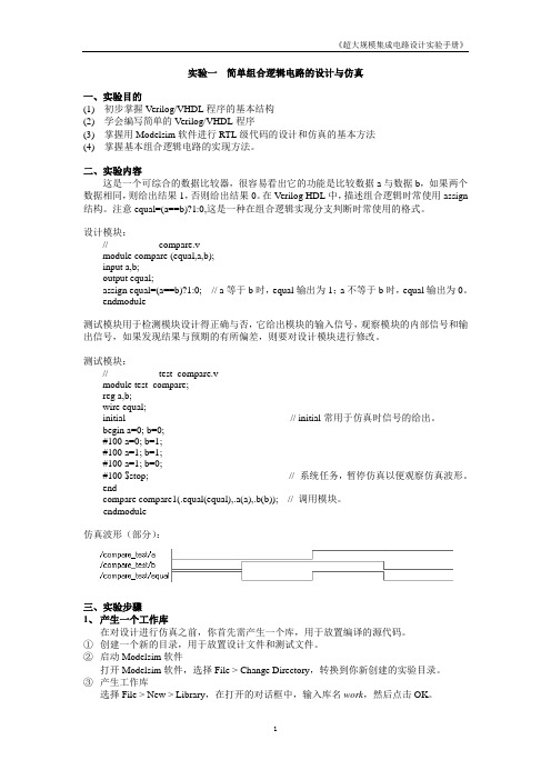
二、实验内容这是一个可综合的数据比较器,很容易看出它的功能是比较数据a与数据b,如果两个数据相同,则给出结果1,否则给出结果0。
在Verilog HDL中,描述组合逻辑时常使用assign 结构。
注意equal=(a==b)?1:0,这是一种在组合逻辑实现分支判断时常使用的格式。
设计模块://--------------- compare.v -----------------------module compare (equal,a,b);input a,b;output equal;assign equal=(a==b)?1:0; // a等于b时,equal输出为1;a不等于b时,equal输出为0。
endmodule测试模块用于检测模块设计得正确与否,它给出模块的输入信号,观察模块的内部信号和输出信号,如果发现结果与预期的有所偏差,则要对设计模块进行修改。
测试模块://--------------- test_compare.v-----------------module test_compare;reg a,b;wire equal;initial // initial常用于仿真时信号的给出。
begin a=0; b=0;#100 a=0; b=1;#100 a=1; b=1;#100 a=1; b=0;#100 $stop; // 系统任务,暂停仿真以便观察仿真波形。
endcompare compare1(.equal(equal),.a(a),.b(b)); // 调用模块。
endmodule仿真波形(部分):三、实验步骤1、产生一个工作库在对设计进行仿真之前,你首先需产生一个库,用于放置编译的源代码。
VCS Lab Guide自学笔记——快速入门VCS

VCS Lab Guide自学笔记——快速入门VCSfrom Monchy(蒙奇)在2020年秋招前根据Synopsys的VCS Lab Guide自学如何VCS(verilog compiled simulation)工具,在此分享前三章详细的学习笔记,几乎是指南的中文翻译,大量的过程截图对初学者很友好。
(VCS Lab Guide是Synopsys给出的VCS官方入门指南,里面包涵源码和实验指导,可以在网上自行下载)1VCS Simulation Basics用VCS编译和仿真8位进位选择加法器的Verilog设计Lab1实验使用8位进位选择加法器。
各模块代码:1fa.v(带进位的一位加法器)2add4.v(带进位4位加法器)3add8.v(8位加法器)4addertb.v(测试平台)代码所在位置如图:Part A:两步仿真过程Task1:用VCS编译verilog源码,生成可执行文件.simvshell>vcs addertb.v fa.v add4.v add8.v如果编译后在终端看到waning,最好先把warning解决了。
Task2:运行testbench,通过simv文件仿真设计shell>./simv如果想要直接通过名字执行必须要先在.bashrc文件中设置。
实际指令是“./simv”,如果没有加“./”刚开始是认不到到。
所以在“.bashrc”文件中加入"export PATH=$PATH:."。
相当与把“./”加入到了PATH中,样再输入“simv”就可以认到了。
具体加到哪我不知道。
task3:使用-o开关重命名可执行文件vcs编译生成的可执行文件的名默认为simv,如果想要改名字需要使用-o开关。
在终端输入下列命令,可以修改simv名字为addertest。
shell>vcs addertb.v fa.v add4.v add8.vPart B:在不同的程序目录下仿真Task1:使用设计库目录编译并仿真addertb.v和add8.v位于/lab1/partb目录下,fa.v和add4.v位于lib库目录内。
vlsi验证

VLSI版图验证实验--基于Dracula工具实验目的:学习VLSI版图验证方法试验任务:完成一个8位adc的版图验证___________________________________________________________ lab1 Drcs设计规则检查一准备任务1传送数据drac.tar 到工作路径,并解包。
2在drac建立设计库project3在drac建立目录../drc。
4拷贝drc.rul文件到../drc5文件如图1:图1二drc.rul设计规则文件处理1 打开drc.rul文件,修改文件中的系统描述为当前描述。
如下:2 输出验证单元dac的gds到../drc.目录3 当前验证单元为dac二运行dracula1 在../drc执行: /IC5/tools/Dracula/bin/PDRACULA2 执行/get ../lvs/lvs.rul3执行/f4执行./lvs/。
等待运行结束。
三查找drc错误和修改错误1用編輯器觀看DRC的結果drc.sum。
2. 尋找OUTPUT CELL SUMMARY 的部分:3. 裏面記錄了那些DRC error?這是什麼樣的DRC error?二使用Dracula Interactive 查找DRC错误1. 回到~/drac 的目錄,進入icfb:2. Library manager : Tools Library Manager…。
3. 打開Lab5/CHIP/layout:在Layout上按中鍵選Open..。
4. 切換到layout editor:Tools layout。
5. 在Virtuoso layout window上執行Dracula Interactive:Tools Dracula Interactive。
6. 設定DRC環境:DRC Setup在DRC Setup form裏Dracula Data Path填入./DRC ,按OK。
vlsi数字集成电路、模拟集成电路的一般设计流程
vlsi数字集成电路、模拟集成电路的一般设计流程VLSI数字集成电路和模拟集成电路的一般设计流程1. 引言在当今数字化社会中,集成电路扮演着至关重要的角色。
VLSI数字集成电路和模拟集成电路的设计流程是实现各种电子产品和系统的关键步骤。
本文将深入探讨这两种集成电路的设计流程,以帮助读者更好地理解其深度和广度。
2. VLSI数字集成电路的一般设计流程2.1 概念阶段在VLSI数字集成电路设计的概念阶段,设计师需要明确定义电路的功能和性能需求。
这一阶段的关键是对电路的整体结构和功能进行描述和规划。
设计师需要考虑的因素包括电路的功耗、速度、面积和可靠性等。
2.2 确定电路结构一旦概念确定,设计师需要开始确定电路的结构。
这涉及到各种模块的设计和连接方式,以满足电路的性能需求。
在这一阶段,设计师需要考虑的因素包括电路的时序、布局、时钟分配以及电源和接地的规划。
2.3 电路设计与仿真确定了电路结构后,设计师需要进行具体的电路设计和仿真。
这一过程涉及到门级电路设计、电路布局、布线、时序分析和电路仿真等环节。
通过仿真和验证,设计师可以发现潜在的问题并进行调整,以确保设计的准确性和可靠性。
2.4 物理验证和制造准备在电路设计和仿真完成后,设计师需要进行物理验证和制造准备。
这一阶段主要包括版图设计、版图修正、DRC/LVS验证、物理仿真和电路的产生等环节。
通过这一过程,设计师可以确保电路的物理实现满足工艺要求和设计规范。
2.5 最终验证和调试设计师需要进行最终验证和调试,以确保VLSI数字集成电路的功能和性能符合设计需求。
这包括设计的逻辑模拟验证、时间域仿真验证、功耗验证以及电路的调试和修正等环节。
通过这一系列步骤,设计师可以最终确认电路的正确性和可靠性。
3. 模拟集成电路的一般设计流程3.1 概念阶段与VLSI数字集成电路类似,模拟集成电路的设计也需要在概念阶段明确定义电路的功能和性能需求。
设计师需要考虑的因素包括电路的增益、带宽、输入/输出阻抗和动态范围等。
lab2操作方法

lab2操作方法
Lab2的操作方法涉及到网络配置,主要包括链路划分和路由配置。
具体操作步骤如下:
1. 二层链路划vlan:按照不同设备进行vlan的划分,如SW3-4的e0/0划为vlan156,e0/1在SW3上划为vlan153,在SW4上划为vlan164。
2. OSPF配置:所有OSPF都需要在接口下宣告。
3. 配置trunk链路:在SW3-6上配置trunk链路,具体操作方式因设备而异。
4. 配置spanning-tree mst:在SW3-6上配置spanning-tree mst,进行mst的配置和命名,以及实例的vlan设置。
以上是Lab2的基本操作步骤,具体细节可能因设备型号和网络环境而有所不同,请根据实际情况进行调整。
如需更多信息,建议咨询专业人士获取帮助。
微电子技术中的超大规模集成电路设计方法

微电子技术中的超大规模集成电路设计方法超大规模集成电路(VLSI)是指具有上百万个晶体管的集成电路。
在微电子技术领域,VLSI设计方法是实现高集成度和高性能的关键因素之一。
本文将介绍一些常用的VLSI设计方法,包括物理设计和逻辑设计。
VLSI的物理设计是将电路设计转化为实际器件的布局和布线。
其中,关键路径优化是物理设计的关键问题之一。
通常,对于高速电路,关键路径上的时延应该尽可能小。
为了达到这个目标,设计工程师可以采用多种技术。
例如,层次布局和多管道化布局可以减少布局中的电气延迟。
另外,时钟树设计也是关键路径优化的一部分。
通过合理的时钟树设计,可以减少时钟信号的延迟和抖动,从而提高电路的工作频率。
此外,VLSI的物理设计还需要考虑功耗优化。
通过采用低功耗器件和电源网络优化技术,可以降低功耗,延长电池寿命。
逻辑设计是将电路功能转化为逻辑元件和电路连接的过程。
在逻辑设计中,设计工程师需要使用硬件描述语言(HDL)来描述电路功能。
常用的HDL包括VHDL和Verilog。
使用HDL,设计工程师可以将电路设计分解为更小的逻辑电路模块,然后将这些模块通过逻辑门、寄存器和触发器等元件进行连接。
在逻辑设计中,设计工程师还需要考虑电路的延迟、功耗和面积等指标。
因此,设计工程师常常需要权衡不同的电路结构和技术参数来优化整个电路的性能。
在VLSI设计过程中,验证是一个非常重要的步骤。
验证是通过仿真、验证和测试来验证电路设计的正确性和可行性。
在仿真过程中,设计工程师可以使用电路仿真工具来验证电路功能的正确性。
通过检查电路输出是否与预期输出一致,设计工程师可以发现并修复电路设计中的错误。
此外,验证还包括对电路的可靠性和容错性进行测试。
通过使用电路测试设备和技术,设计工程师可以检测电路的性能和可靠性,并确保电路在不同工作条件下都能正常工作。
除了物理设计、逻辑设计和验证,VLSI设计还涉及到一些其他的问题。
例如,VLSI设计中的数据通信和互连问题是一个关键的挑战。
vlsi设计cad工具Chapter2 ICFB

Chapter 2Cadence ICFBCADENCE is a large company that offers a dizzying array of software for Electronic Design Automation (EDA)or Computer Aided De-sign (CAD)applications.Cadence CAD software is generally The custom design tutorials are a good starting point for custom analog IC design too targeted at the design of electrical circuits,both digital and analog,and extending from extremely low-level VLSI design to the design of circuit boards for large systems.This book is primarily interested in digital inte-grated circuit (IC)design so we’ll look primarily at those tools from the Cadence suite.2.1Cadence Design FrameworkMany of the digital IC design tools from Cadence are grouped under a framework called Design Framework II (dfII ).The dfII environment in-tegrates a variety of design activities including schematic capture (Com-poser ),simulation (Verilog-XL or NC Verilog ),layout design (Virtuoso and Virtuoso-XL ,design rule checking (DRC)(Diva and Assura ),layout versus schematic checking (LVS)(Diva and Assura ),and abstract gen-eration for standard cell generation (Abstract ).These are all individual programs that perform a piece of the digital IC design process,but are all accessible (to a greater or lesser extent)through the dfII framework and the dfII user interface.Note that many of these programs were developed by separate companies that have been acquired by Cadence and folded into the dfII framework after that acquisition.Thus,some integrate better than others!As we’ll see,though,there are some pieces of the Cadence tool flow that are not linked into the dfII framework.Most notably place and route of standard cells with SOC Encounter ,connection of large blocks with ICC Chip Assembly Router (CAR)and Verilog synthesis with BuildGatesCHAPTER2:Cadence ICFB Draft August24,2006are done in separate programs with separate interfaces.However,we’ll start with the dfII tools in this toolflow,so we’ll need to start up the dfII framework.The executable in the Cadence tool suite thatstarts up this framework is called icfb which stands for Integrated CircuitFront to Back design.If you were to set up your search path so that theCadence tools were on your path,and execute the icfb command youwould see the dfII framework start up.Unfortunately,this wouldn’t help you much!It turns out that having the tool framework is only half the battle.You also need detailed technologyinformation about the devices you want to use for your design.This detaileddesign information includes technology information about the IC processthat you are using and libraries of transistors,gates,or larger modules thatyou can use to build your circuits.This information includes manyfiles ofdetailed(and somewhat inscrutable)information,and does not come fromCadence.Instead,it comes from the vendor of the IC process and from thevendor of the gate and module cells that you are using in your design.Thiscollection design information is typically called a“Cadence Design Kit”orCDK.For this book we will use technology information for IC processes sup-ported by the MOSIS chip fabrication service.This information has beenassembled into a CDK by the good folks at North Carolina State University(NCSU).The NCSU CDK has detailed techology information for all the We’re usingNCSU CDK v1.5processes currently offered through MOSIS.These processes are available either in“vendor”rules which have have the actual specifics of the technol-ogy as offered by the vendor,or through abstracted rules known as ScalableCMOS or SCMOS rules.The SCMOS are scalable in the sense that a de-sign done in the SCMOS rules should,theoretically,be useable in any of theMOSIS processes simply by changing a scalaing parameter.That means thatthe SCMOS rules are a little conservative compared to some of the vendorrules because they have to work for all the different vendors.Of course,it’s not quite that simple because as design features get smaller and smaller the IC structures don’t scale at the same rate.But,it workspretty well.To handle the differences required by smaller geometry pro-cesses MOSIS has a number of modifiers to the SCMOS rules(SCMOSfor“generic”SCMOS,SCMOS SUBM for submicron processes,and SC-MOS DEEP for even smaller processes).For this class we’ll be using the We’re using theSCMOS V8.0rules.SCMOS SUBM rules which will then be fabricated on the AMI C5N0.5µCMOS process.But,that’s getting ahead of ourselves a little bit.The important thing for now is that without the NCSU CDK,we won’t have any technology infor-mation to work with.So,instead of starting up icfb directly,we’ll start it upwith the NCSU CDK already loaded.This will happen by calling Cadence16Draft August 24,2006 2.2:Starting Cadencefrom a script that we’ve written instead of calling the tool directly.This script will start a new shell,set a bunch of required environment variables,and call the icfb tool with the right switches set.Other tools for the rest of this book will use similar scripts.2.2Starting CadenceBefore you start using cadence you need to complete the following steps:First make a directory from which to run Cadence.This is important so that all of Cadence’s files end up in a consistent location.It’s also nice to have all of Cadence’s setup and data files in a subdirectory and not clogging up your home directory.I recommend making an IC CAD directory and CAD tools can generate a lot of temporary and auxiliary files!then under that making a cadence ter on we’ll add to that by making separate directories for the other IC tools like Synopsys dc shell,module complier,SOC Encounter and so on under that IC CAD directory.c dmkdir IC CADmkdir IC CAD/cadenceNow it’s handy to set a few environment variables.In particular you want to set your UNIX search path to include the directory that has the startup scripts for the CAD tools.You also need to set an environment vari-able that points to a location for class-specific modifications to the general Cadence configuration files.I recommend that you put these commands in your .cshrc or .tcshrc file so you won’t have to retype them each time you start a shell.If you’re using bash you’ll have to adjust the syntax slightly,and if you’re not at the University of Utah these paths will be different.s et path =($path /uusoc/facility/cad common/local/bin/F06)setenv LOCAL CADSETUP /uusoc/facility/cad common/local/class/6710By default the tool scripts will start the tool in the directory that you are connected to when you execute the script.If you’d like to have All the Cadence and Synopsys CAD tools run on Solaris or Linux so if you don’t have a good grasp of basic UNIX commands,now’s the time to go learn them!Cadence connect to a specific directory automatcally every time you execute the script you can set your CADENCEDIR environment variable.This way you don’t have to remember to connect to your $HOME/IC CAD/cadence directory each time (but it means you can’t have different directories for different projects without unsetting that environment variable):s etenv CADENCEDIR $HOME/IC CAD/cadenceFinally,you need to copy one Cadence init file from the NCSU CSK directory so that things get initialized correctly.The file is called .cdsinit17CHAPTER2:Cadence ICFB Draft August24,2006(note the initial dot!).You can put it in your$HOME directory so thatyou’ll always get that initfile,or you can put it in the directory from whichyou start Cadence if you think you might ever want to start Cadence froma different directory for different projects or classes with a different.cdsinitfile.I recommend making this a symbolic link so that if the system-wide.cdsinitfile is updated you’ll see the new version automatically.Again,ifyou’re not at the University of Utah these paths will be different.l n-s/uusoc/facility/cad common/NCSU/CDK-F06/.cdsinit$HOMEorcd$HOME/IC CAD/cadenceln-s/uusoc/facility/cad common/NCSU/CDK-F06/.cdsinit.Now that you have your own cadence directory(called$HOME/IC CAD/cadence if you’ve followed the directions up to this point),set your path,and linked the NCSU.cdsinitfile either to$HOME or to$HOME/IC CAD/cadence you’re ready to start Cadence icfb with the NCSUCDK.If you’ve set your environment variable CADENCEDIR then the classscripts will also connect you to the right working directory each time youstart the tools.If not,please connect to your$HOME/IC CAD/cadence di-rectory(or where ever you wish to start Cadence from)first.Start Cadence with the command:c ad-ncsuOf course,once you set this all up once,you should be able to jump We’re using dfII fromthe IC v5.1.41release right to the cad-ncsu step the next time you want to start Cadence.You should see two windows once things get started up.Thefirst is the Command Interperter Window or CIW.It’s shown in Figure2.1.Theother is the Library Manager shown in Figure2.2.The CIW is the maincommand interface for all the dfII tools.In practice you will probably nottype commands into this window.Instead you’ll use interfaces in each of thetools themselves.However,because most of the tools put their dignostic Cadence also keeps thelog information in a CDS.logfile which it puts in your$HOMEdirectory log information into the CIW,you will refer back to it often.Also,there are some things that just have to be done from this window.For now,just make sure that your CIW looks something like the one in Figure2.1.The Library Manager is a general interface to all the libraries and cells views that you’ll use in dfII.Cells in dfII are individual circuits that you want to design separately.In dfII there is a notion of a“cell view”which means that you can look at a cell in a number of different ways(in different views).For example,you might have a shematic view that shows the cell in terms of its components in a graphical schematic,or you might have a18Draft August24,2006 2.2:Starting CadenceFigure2.1:Command Interperter Window(CIW)for cad-ncsu Verilog description of the cell as behavioral Verilog code.Both of these cell views can exist at the same time and are just alternate ways of looking at the same cell.The cell views that we’ll eventually end up using in this toolflow are the following:schematic:This view is a graphical schematic showing a cell as an inter-connection of basic components,or as hierarchically defined compo-nents.symbol:This view is a symbolic view of the cell that can be used to place an instance of this cell in another schematic.This is the primary mecha-nism for generaing hierarchy in a schematic.cmos sch:This is a schematic that consists of CMOS transistors.A cmos sch view corresponds to a cell that is completely contained in a singlestandard cell.That is,it is a leaf-cell in the standard cell hierarchythat corrseponds to a cell in an existing library.It’s important in sometool steps to differentiate the schematics that should be expanded bythe netlisting process and the leaf cells where the netlisting shouldstop.That’s the purpose of the cmos sch view.extracted:This view is generated by the circuit extraction process in the Cadence tools.It contains an extracted electrical netlist of the cellthat the simultors can use to understand the electrical behavior of thecell.analog-extracted:This view is generated from the extracted view and con-tains a little extra information for the analog simulator. behavioral:This view is Verilog code that describes the behavior of the cell.19CHAPTER2:Cadence ICFB Draft August24,2006Figure2.2:Library Manager window in cad-ncsulayout:This view contains the composite layout information for a cmos sch cell.This is the graphical information that the IC fabrication service uses to fabricate the cell on the silicon.abstract:This layer takes the layout and extracts only the informaton that the place and route software needs to do the placement and routing.That is,it needs to know the physical dimensions of the cell,the con-nection points and layers,and any obstructions for the metal routing layers,but it doesn’t need to know anything about the transistor lay-ers.This view will be generated by the abstract process.functional:This view is reserved for behavioral descriptions of CMOS transistors.It’s used for a similar reason to the cmos sch view:it lets the netlister know when it has hit a transistor.You won’t need to create these views unless you’re adding new transistor models to a library.spectre:This view is used by the analog circuit netlister to generate an in-putfile for the Spectre analog simulator.You won’t need to create this20Draft August 24,2006 2.2:Starting Cadenceview unless you’re adding new transistor models to a library.There are a number of other similar views for other simulators that you also don’t need to worry about.A “library”is a collection of cells that are grouped together for some reason (being part of the same project,or part the same set of standard cells,for example).Libraries also have technology information attached to them so that the cells in the library refer to a consistent set of technolgy data.This technology information is linked rather than copied so that when updates are made on the techology,all libraries with that technology at-tached will see the updates.For example,all the standard gates cells that The UofU Digital library uses the v11syntax to indicate version 1.1of the library.Cadence doesn’t like dots in cell names!you’ll be using (until you make your own!)are grouped into a library called UofU Digital v11.You will create libraries for each of your designs so that you can keep the design data separate for different projects.Think of librarires as directories that collect design dat together for a specific design.You could throw all your stuff into one directory,but it would be easier to find and use if you separate different designs into different libraries.You should see a bunch of libraries already listed in the Library Man-ager.If you scroll around you should be able to see the following:NCSU TechLib xxx:These are technology libraries for each of the MO-SIS processes.The “xxx”will be filled in with information about which MOSIS process is being desctribed.We won’t use these di-rectly,and depending on how Cadence is set up for your class you might not see these at all.If you’re not using the UofU packages,then you’ll probably see all of these.NCSU Analog Parts:This library contains components (transistors,resis-tors,capacitors,etc.)that we’ll use for transistor-level design,and also some components for circuit-level simulation using spectre (in the Affirma analog circuit design environment).The switch-level transistor models in this library have zero delay for simulation.NCSU Digital Parts:This library contains a variety of Boolean logic gatesthat you can use for gate-level design.Note that these gates do not have layout or place and route views so they can not be used for ac-tually building chips!They will be used in this class just for the initial “learn about the schematic capture tool”assignment.basic:This is the Cadence built-in library which you won’t use directly.cdsDefTechLib:A generic Cadence technology that we won’t use.UofU Analog Parts:This is a library with copies of the transistor com-ponents from the NCSU Analog Library ,but these transistors have 0.1ns of delay for switch level simulation.21CHAPTER2:Cadence ICFB Draft August24,2006UofU TechLib ami06:This is a technology library for the AMI C5N0.5µlibrary using the SCMOS SUBM rules that we’ll use in the tutorials.It’s based on the NCSU technology library for this process,but hassome local tweaks that make it a little more friendly to thisflow.UofU Sheets:This library has graphics for schematic sheet borders.UofU Digital v11:This is a library of standard cells developed at the If you look at the cells inUofU Digital v11you should see that each of them has a number of different cell views as defined previouslyUniversity of Utah for VLSI classes.It has the UofU TechLib ami06 technology attached to it so it can be used with the AMI C5N0.5µCMOS process through the SCMOS SUBM design rules from MO-SIS.This will all make more sense later...Unfortunately,you’ll have to keep very careful track of when to use components out of each of these libraries.Some have very specific uses. The only way to handle this is just to pay attention and keep track!Now that you’ve started Cadence using the cad-ncsu script,we can move on to using the individual EDA tools in the dfII suite...22。
VLSI基础实验ppt2

单击OK后,有一个较长的综合过程,综合时间的长 短取决于设计的大小和时序的约束等情况,请耐心等候。 综合完毕后,出现下面的网表图2-21。
(三)、实验步骤 )、实验步骤: 实验步骤
(三)、实验步骤 )、实验步骤: 实验步骤
具体实验操作步骤如下: ①、启动Design Compiler综合器,打开命令输入窗口。在 工作站上登陆,并打开一个Terminal。 进入综合环境。在 命令提示符下输入 design_vision&。
(三)、实验步骤 )、实验步骤: 实验步骤
此时会弹出一个如下图所示的窗口,该窗口为Design Compiler综合工具的图形界面。
选择并加载用户设计源文件,如图2-12。
(三)、实验步骤 )、实验步骤: 实验步骤
用户设计源文件加载后,进行实现(Elaborate)。这 里的实现和接下来的综合是有很大区别的,实现只是将设 计用Design Compiler自带的广义综合库进行实现,并未 映射到厂商的逻辑单元库。打开File-Elaborate,如下图213。
(三)、实验步骤 )、实验步骤: 实验步骤
导出时序信息文件。操作如下图2-24,打开File-Save info。
(三)、实验步骤 )、实验步骤: 实验步骤
选择路径及文件名,如图2-25。
(三)、实验步骤 )、实验步骤: 实验步骤
由于在下一步使用Astro进行自动布局布线时需要使用后缀名为 sdc的时序文件,因此可在DC的命令操作提示行内输入write_sdc + 存储路径/目标时序文件名来得到该时序文件,如果不输入存储路径则 默认将该sdc时序文件存储在当前启动DC的操作路径目录下。 至此,ASIC逻辑综合完成,并通过综合获得了逻辑电路图、进行 自动布局布线所需的逻辑电路网表文件和时延信息文件。 需要注意的是,在此处所使用的综合库文件一定要和在下一步操 作中使用的自动布局布线所使用的工艺库是同一家工艺厂商提供的综 合库,否则即使DC综合所得网表是正确的,也无法正确的进行下一 步自动布局布线的操作。使用DC的具体方法可以参考《计算机仿真 技术》课程的实验指导书。
- 1、下载文档前请自行甄别文档内容的完整性,平台不提供额外的编辑、内容补充、找答案等附加服务。
- 2、"仅部分预览"的文档,不可在线预览部分如存在完整性等问题,可反馈申请退款(可完整预览的文档不适用该条件!)。
- 3、如文档侵犯您的权益,请联系客服反馈,我们会尽快为您处理(人工客服工作时间:9:00-18:30)。
VLSI Design Lab 2Due to 4/6 pm 12:00Setup1. %cd T181p6m_ads%cp .cdsinit ../ (run calibre需使用之檔案) %icfb&1.1 Tool=> Library manager1.2 File=>New=>Library1.3輸入library name然後按OK3. File=>New=>Cell View1.4 直接選OK1.5Create Schematic2.4選擇剛剛建好的librar y,然後選File=>New=>Cell View2.5如下圖Tool=>Composer Schematic,然後輸入Cell Name3Add component利用軟體中預設的library (analogLib與basic)已定義好的元件完成schematic viewChoose: Add->Instance就會看到對話window,再選取Browse中之analogLib之元件,即可.Note:Tsmc or Umc通常會提供pcell. 同理,Add->Pin,but must define input terminal and output terminal pin.(vdd and gnd 屬於inoutput)最後用Add->Wire做接線的動作即可。
4Using Parameterized Cell (Pcell)選tsmc18rf的Library 使用pmos2v、nmos2v 之MOS元件(為了之後LAYOUT會用到)。
L為channel length 、W為channel width5Syntax check完成電路圖後要做CHEC K,與之後做LVS(Layout V.S Schematic )會有關係,當接線及電路元件都兜完後,Choose: Design->Check and Save 觀察CIW上的message直到schematic電路皆無錯誤後電路才算完成Example 1:不可以3條線連在同一點。
Example 2:no error --->完成Layout Editor1.選擇之前建好的librar y,然後選File=>New=>Cell View 接下來C ell View => VirtuosoOption => DisplayOptions => Layout Editor 132設定游標靠近object時即被吸引到object的邊緣:建議不要勾選Set gravity on 之control typeSet gravityon時所能影響之範圍在為幾個unit之內熱鍵(有分大小寫)k -Ruler Shift+k -取消尺規r -Rectangle (用來畫連線)o -用來畫兩層間contact 及via(常用) m -Move c -Copy s -Stretch Shift+z -Zoom out Ctrl+z -Zoom in f -Fit Editshift+f & ctrl+f -switching instance view Key+F3 –每個功能之詳細設定3.1 Create =>Instance提供設計者可以把設計好的layout Cell 直接叫進來使用,選: Creative->Instance ,再選取Browse 中設計好的Cell 或pcell 之元件即可。
3.2 Creative->Label (對應到schematic 的pin ;在Calibre 之LVS 驗證裡layout 是認label )。
Note:不可以打在poly 上4. Layout XLAuto-drawing pcell layout but not include wire connectio nTool=>Layout XL先選材質: 打在METAL1 就要選METAL1Invoke a schematic windo w:First choose a MOS form the Schematic window then Create=>Pick from Schematic then drag to layout window.Verification Using CalibreDesign Rule Checking(DRC)1. Using Calibre DRC Tool Calibre=>Run DRC1.指定DRC rule 的路徑2.指定跑DRC 時資料要存放的路徑3.載入之前run DRC 時的設定(optional) 1.1 先按Cancel 關掉 Load Runset File 視窗, 因為第一次使用並無此檔案。
1.2 DRC rule 的路徑請選擇/home/raid1_2/userd/d93020/T181p6m_ads /DRC/Calibre_DRC-1_3A2_5C_modify /T18_Calibre_DRC_13A25C_modify 不要按Load(藍色部分每個人不同)2.Inputs如果已經有轉好的gds 檔則可以 不選Export form layout view。
(gds檔為layout所轉出之檔案)3. Outputs使用預設就好。
3. Run DRCRun 完後會跑出下面視窗Debu g:DRC REV Erase errorhighlight errorerror descriptionerror position error number4.每次run DRC check前要關掉DRC REV視窗。
5.要關掉Calibre Interactiv時,可以把設定存起來NOTE:以下為可忽略之DRC ERROR皆為DENSITY之ERROR。
但是當要下線時則需要考慮Layout v.s. Schematic1.Calibre InteractiveUsing Calibre LVS ToolCalibre=>Run LVS1.指定LVSrule的路徑2.指定跑LVS時資料要存放的路徑3.載入之前run DRC時的設定(optional)LVS rule的路徑請選擇home/raid1_2/userd/d93020/T181p6m_ads/LVS/Calibre_LVS-1_3A/T18_Calibre_LVS_13A.13a不要按Load(藍色部分每個人不同)2.如果已經有轉好的gds檔則可以不選export from layout viewer;如只修改schematic則可以不選。
3.如果已經有轉好的netlist檔則可以不選export from schematic viewer;如只修改layout則可以不選。
4. RUN LVS跑完LVS 會出現下面視窗:LVS REV下圖為LVS report (文字模式顯示比對結果及錯誤訊息)IncorrectnessCorrectness5. Debug使用LVS REV視窗來修正layout與schematic不match的地方Example:用滑鼠點錯的地方則layout會highlight。
error description: schematic裡的OUT & net8分別連到不同的線,而在layout裡卻有1條線連到Layout Parameter Extraction1.先修改下述檔案第2136行/home/raid1_2/userd/d93020/T181p6m_ads/LPE/Calibre_LPE-1_3A/T18_Calibre_L PE_13A.13ainclude /home/raid1_2/userd/d93020/T181p6m_ads/LPE/Calibre_LPE-1_3A/rules藍色粗體部份改成自己的路徑(可以先使用UltraEdit軟體改好再上傳)1.1 Calibre InteractiveUsing Calibre LPE ToolCalibre=>Run PEX1.指定LPE rule的路徑2.指定跑LPE時資料要存放的路徑3.載入之前run DRC時的設定(optional)LPE rule的路徑請選擇/home/raid1_2/userd/d93020/T181p6m_ads/LPE/Calibre_LPE-1_3A/T18_Calibre_L PE_13A.13a不要按Load(藍色部分每個人不同)2. Inputs已經有轉好的gds檔則可以不選export from layout viewer;如只修改schematic則可以不選。
3 OutputsFORMAT:選HSPIC E。
FILE:OUTPUT FILE可以改成*.sp。
Use Name From:會根據你選的來源把Pin&net的名稱mapping到out file的netlist;可以選LAYOUT or SCHEMATIC。
Extraction Typ e:選Transistor Level;RC or R。
Output netlist:為sub-circuit格式且會把extract出來的RC檔案include進來。
4.Run PEX5.把轉出來的netlist拿來做post-simulation,如果p erformance有差很多就要再修改layout or你的設計。
Inverter schematic & layout view (TSMC 0.18um)Layout常見問題1.為什麼不行選layer檢查是否接換到大寫模式也就是鍵盤Cap Lock燈是亮的。
2.為什麼undo只能3次Options=>User PreferenceBuilding Basic Logic Cell1. It can make the layout fast, regular ,and clear.->Easy to debug2. It like cell base design.->Only need connectionExample (MCLA)Schematic viewLayout view:The red blocks are instances.Create symbol from Schematic1.前面已說明如何建立一個電路的scmemati c,因為要使用cell的觀念來建立較大的電路,因此以使用symbol的方法來建立schematic2.打開之前建立的schematic;Design=>Create Cellview=>from Cellview選OK3. Pin Specification:分配pin的位置4. 完成後點sav e,之後便可以使用instance的方式來建立schematic5. 如果schematic有做修改,如增加或修改pin的名稱,則需要從重做上述步驟,此外還要額外做Cross View Check。