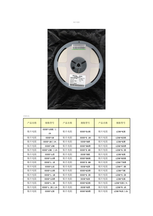
四川永星厚膜片式电阻器选型手册
贴片电阻型号及选用方法
贴片电阻详细信息:类型参考国际的分类常规系列厚膜贴片电阻General purpose General purpose, 0201 - 0805General purpose, 1206 - 2512高精度高稳定性贴片电阻High precision - high stability High precision - high stability, 0201 - 0603 High precision - high stability, 0805 - 1210High precision - high stability, 2010 - 2512高精密贴片电阻- AR 系列的特性与用途-超精密性±0.01% ~ ±1%-TaN 和NiCr 真空溅镀-温度系数只有±5PPM/°C ~ ±50PPM/°C-Wide R-Value range-Products with Pb-free Terminations Meet RoHS Requirments常应用于-医疗设备-精密量测仪器-电子通讯,转换器,印表机-Automatic Equipment Controller-Communication Device, Cell phone, GPS, PDA-一般消费性产品常规系列薄膜贴片电阻General purpose thin film General purpose thin film, 0201-2512低阻值贴片电阻Low ohmic Low ohmic, 0402 - 1206Low ohmic, 2010 - 2512贴片电阻阵列Arrays Arrays, convex and concave贴片电流传感器SMD current sensors Current Sensors - Low TCR贴片网络电阻器Network Network, T-type and L-type另有贴片厚膜排阻,贴片打线电阻,贴片高压电阻,贴片功率电阻等!片式固定电阻器,从Chip Fixed Resistor直接翻译过来的,俗称贴片电阻(SMD Resistor),是金属玻璃铀电阻器中的一种。
固定厚膜贴片电阻器; 矩形型和高功率抗浪涌 RPCH16,20,32,35说明书

No.: RPCH-K-HTS-0001 /2Date: 2017.4.21Data sheetTitle: FIXED THICK FILM CHIP RESISTORS; RECTANGULAR TYPE AND HIGH POWER ⋅ ANTI SURGEStyle: RPCH16,20,32,35AEC-Q200 qualifiedRoHS COMPLIANCE ITEMHalogen and Antimony FreeNote: ・Stock conditionsTemperature: +5°C ∼+35°CRelative humidity: 25% ∼ 75%The period of guarantee: Within 2 year from shipmen t by the company.Solderability shall be satisfied.・Product specification contained in this data sheetare subject to change at any time without notice・If you have any questions or a Purchasing Specification for any quality Agreement is necessary, please contact our sales staff. ArrayHokkaido Research CenterApproval by: T. SannomiyaDrawing by: M. Shibuya1. Scope1.1 This data sheet covers the detail requirements for fixed thick film chip resistors; rectangular type & high power ⋅ anti surge,style of RPCH16,20,32,35.1.2 Applicable documentsJIS C 5201−1: 2011, JIS C 5201−8: 2014, JIS C 5201−8−1: 2014 IEC60115−1: 2008, IEC60115−8: 2009, IEC60115−8−1: 2014 EIAJ RC −2134C −20102. ClassificationType designation shall be the following form.(Example) RPCH 32 K 123 J TP 1 2 3 4 5 6 Style1 Fixed thick film chip resistors; rectangular type & & high power ⋅ anti surge2 Rated dissipation and / or dimension3 T emperature coefficient of resistance4 Rated resistance123 E24 Series, 3 digit, Ex. 123--> 12k Ω, 1000 E96 Series, 4 digit, Ex. 1000-->100Ω1022--> 10.2k Ω5 T olerance on rated resistanceD ±0.5% F ±1% J ±5%6 Packaging formB Bulk (loose package) TP Paper taping TE Embossed tapingK ±100×10−6/ °C−(Dash ) Standard Style3. Rating3.1 The ratings shall be in accordance with T able −1.T able −1StyleRated dissipation (W) T emperature coefficient of resistance (10-6 / °C) Rated resistance range (Ω)Preferred number series for resistors T olerance on rated resistance RPCH160.33K ±100 10∼1M E24, 96 D(±0.5%), F(±1%) Standard ±200 1.0∼9.76 K ±100 10∼1M E24 J(±5%) Standard ±200 1.0∼9.1 RPCH20 0.5K ±100 10∼1M E24, 96 D(±0.5%), F(±1%) Standard ±200 1.0∼9.76 K ±100 10∼1M E24 J(±5%) Standard ±200 1.0∼9.1 RPCH32 0.66K ±100 10∼1M E24, 96 D(±0.5%), F(±1%) Standard ±200 1.0∼9.76 K ±100 10∼1M E24 J(±5%) Standard ±200 1.0∼9.1 RPCH35 0.75K ±100 10∼1M E24, 96 D(±0.5%), F(±1%) Standard ±200 1.0∼9.76 K ±100 10∼1M E24J(±5%)Standard±200 1.0∼9.1Style Limiting element voltage(V) Isolation voltage(V) Category temperaturerange(°C)RPCH16 150150 −55~+155RPCH20200500RPCH32 RPCH353.2 Climatic category55/155/56 Lower category temperature − 55 °C Upper category temperature +155 °C Duration of the damp heat, steady state test 56days 3.3 Stability class5% Limits for change of resistance:−for long −term tests ±(5%+0.1Ω) −for short −term tests ±(1%+0.05Ω)3.4 DeratingFigure–1 Derating curveAmbient temperature (°C)3.5 Rated voltaged.c.or a.c.r.m.s.voltage calculated from the square root of the product of the rated resistance and the rated dissipation. E: Rated voltage (V)E =P ·RP: Rated dissipation (W) R: Rated resistance (Ω)Limiting element voltage can only be applied to resistors when the resistance value is equal to or higher than the criticalresistance value.At high value of resistance, the rated voltage may not be applicable.4. Packaging formThe standard packaging form shall be in accordance with T able −2.T able −2Symbol Packaging form Standard packagingquantity / unitsApplicationB Bulk (loose package) 1,000 pcs .RPCH16,20,32,35 TP Paper taping 8mm width, 4mm pitches 5,000 pcs. RPCH16,20,32TE Embossed taping8mm width, 4mm pitches 4,000 pcs. RPCH355. Dimensions5.1 The resistor shall be of the design and physical dimensions in accordance with Figure −2 and T able −3.Figure −2T able −3 Unit: mmStyle L W H c d RPCH16 1.6±0.1 +0.15 0.8 -0.05 0.45±0.10 0.3±0.2 0.3±0.1 RPCH20 2.0±0.1 1.25±0.10 0.55±0.10 0.3±0.2 0.4±0.2 RPCH32 3.1±0.1 1.6±0.15 0.55±0.10 0.4±0.25 0.5±0.25 RPCH35 3.1±0.15 2.5±0.15 0.55±0.15 0.4±0.25 0.5±0.255.2 Net weight (Reference)Style Net weight(mg) RPCH16 2 RPCH20 5 RPCH32 9 RPCH35 166. MarkingResistorThe Rated resistance shall be marked in 3 digits (E24) or 4 digits (E96) and marked on over coat side.• E24 series: 3 digits, E96 series: 4 digitsIn case of the resistance value that E96 overlaps with E24, It is marked by either.The Rated resistance of RPCH16 should not be marked in 4 digits(E96)Marking example Contents Application123 12×10 3 [Ω]→ 12 [kΩ]E24(RPCH16,20,32,35)2R2 2. 2[Ω]E24(RPCH 16,20,32,35)5623 562 ×103 [Ω] → 562 [kΩ] E96(RPCH 20,32,35)12R7 12.7 [Ω] E96(RPCH 20,32,35)7. Performance7.1 The standard condition for tests shall be in accordance with Sub−clause 4.2, JIS C 5201−1: 2011.7.2 The performance shall be satisfied in T able−4.T able−4(1)No. T est items Condition of test (JIS C 5201−1) Performance requirements1 Visual examination Sub−clause 4.4.1Checked by visual examination. As in 4.4.1The marking shall be legible, as checked by visual examination.2 DimensionResistance Sub−clause 4.4.2Sub−clause 4.5As specified in T able−3 of thisspecification.As in 4.5.2The resistance value shallcorrespond with the rated resistancetaking into account the specifiedtolerance.3 Voltage proof Sub−clause 4.7Method: 4.6.1.4T est voltage: Alternating voltage with a peakvalue of 1.42 times the insulationvoltage.Duration: 60 s ± 5 sInsulation resistanceT est voltage: Insulation voltageDuration: 1 min. No breakdown or flash over R ≥ 1 G Ω4 Solderability Sub−clause 4.17Without ageingFlux: The resistors shall be immersed in anon−activated soldering flux for 2s.Bath temperature: 235 °C ± 5 °CImmersion time: 2 s ± 0.5 s As in 4.17.4.5The terminations shall be covered with a smooth and bright solder coating.T able −4(2)No T est items Condition of test (JIS C 5201−1)Performance requirements 5Mounting Overload (in the mounted state) Solvent resistance of the marking Sub −clause 4.31 Substrate material: Epoxide woven glass Sub −clause 4.13 The applied voltage shall be 2.5 times the rated voltage or twice the limiting element voltage, whichever is the less severe. Duration: 2 s Visual examination ResistanceSub −clause 4.30 Solvent: 2−propanolSolvent temperature: 23 °C ± 5 °C Method 1Rubbing material: cotton wool Without recoveryNo visible damage ∆R ≤ ± (1%+0.05Ω) Legible marking6Mounting Bound strength of the end face plating Final measurements Sub −clause 4.31 Substrate material: Epoxide woven glass Sub −clause 4.33 Bent value: 3 mm Resistance Sub −clause 4.33.6 Visual examination∆R ≤ ± (1%+0.05Ω) No visible damage7Resistance to soldering heat Component solvent resistance Sub −clause 4.18 Solder temperature: 260 °C ± 5 °C Immersion time: 10 s ± 0.5 s Visual examination Resistance Sub −clause 4.29 Solvent: 2−propanolSolvent temperature: 23 °C ± 5 °C Method 2Recovery: 48 h Visual examination ResistanceAs in 4.18.3.4No sign of damage such as cracks. ∆R ≤ ± (1%+0.05Ω)No visible damage ∆R ≤ ± (1%+0.05Ω)T able −4(3)No T est itemsCondition of test (JIS C 5201−1)Performance requirements 8MountingAdhesionRapid change temperatureSub −clause 4.31Substrate material: Epoxide woven glass Sub −clause 4.32 Force: 5 NDuration: 10 s ± 1 s Visual examination Sub −clause 4.19Lower category temperature:−55 °C Upper category temperature:+155 °CDuration of exposure at each temperature: 30 min.Number of cycles: 5 cycles. Visual examination ResistanceNo visible damageNo visible damage ∆R ≤ ±(1%+0.05Ω) 9Climatic sequence −Dry heat−Damp heat, cycle (12+12hour cycle) First cycle−Cold−Damp heat, cycle (12+12hour cycle) Remaining cycle−D.C. loadSub −clause 4.23 Sub −clause 4.23.2T est temperature: +155 °C Duration: 16 h Sub −clause 4.23.3 T est method: 2T est temperature: 55 °C [Severity(2)]Sub −clause 4.23.4T est temperature −55 °C Duration: 2hSub −clause 4.23.6 T est method: 2T est temperature: 55 °C [Severity (2)]Number of cycles: 5 cycles Sub −clause 4.23.7The applied voltage shall be the rated voltage or the limiting element voltage whichever is the smaller.Duration: 1 min. Visual examination ResistanceNo visible damage ∆R ≤ ± (5%+0.1Ω) 10MountingEndurance at 70 °C Sub −clause 4.31Substrate material: Epoxide woven glass Sub −clause 4.25.1Ambient temperature: 70 °C ± 2 °C Duration: 1000 hThe voltage shall be applied in cycles of 1.5 h on and 0.5 h.The applied voltage shall be the rated voltage or the limiting element voltage whichever is the smaller.Examination at 48 h , 500 h and 1000 h:Visual examination ResistanceNo visible damage ∆R ≤ ± (5%+0.1Ω)T able −4(4)No T est items Condition of test (JIS C 5201−1)Performance requirements 11Mounting V ariation of resistance with temperature Sub −clause 4.31 Substrate material: Epoxide woven glass Sub −clause 4.8 −55 °C / +20 °C+20 °C / +155°CAs in T able −112Mounting Damp heat, steady state Sub −clause 4.31 Substrate material: Epoxide woven glass Sub −clause 4.24Ambient temperature: 40 °C ± 2 °C +2 Relative humidity : 93 % −3 a) 1st group: without voltage applied.b) 2nd group: The d. c. voltage shall be appliedcontinuously .The voltage shall be accordance with Sub −clause 4.24.2.1 b). without polarizing voltage [4.24.2.1, c)] Visual examinationResistanceNo visible damage Legible marking ∆R ≤ ± (5%+0.1Ω) 13Dimensions (detail) Mounting Endurance at upper category temperature Sub −clause 4.4.3 Sub −clause 4.31 Substrate material: Epoxide woven glass Sub −clause 4.25.3 Ambient temperature:155 °C ± 2 °CDuration: 1000 hExamination at 48 h, 500 h and 1000 h:Visual examination Resistance As in T able −3No visible damage ∆R ≤ ± (5%+0.1Ω)8. T aping8.1 Applicable documents JIS C 0806−3: 2014, EIAJ ET −7200C: 2010 8.2 T aping dimensions8.2.1 T aping dimensions shall be in accordance with Figure −3 and T able −5.Unit: mmFigure −3T able −5 Unit: mmStyle A B t 1 t 2 RPCH16 1.15±0.15 1.9±0.2 0.6±0.1 0.8max. RPCH20 1.65±0.15 2.5±0.2 0.8±0.1 1.0max. RPCH32 2.00±0.15 3.6±0.2 0.8±0.1 1.0max.8.2.2 Embossed taping dimensions shall be in accordance with Figure −4 and T able −6.Unit: mmFigure −4T able −6 Unit: mmStyle A B W E t 1 RPCH35 2.85±0.20 3.5±0.2 8.0±0.3 3.5±0.05 1.0±0.21). The cover tapes shall not cover the sprocket holes.2). T apes in adjacent layers shall not stick together in the packing. 3). Components shall not stick to the carrier tape or to the cover tape. 4). Pitch tolerance over any 10 pitches ±0.2mm.5). The peel strength of the top cover tape shall be with in 0.1N to 0.5N on the test method as shown in the followingRPCH16,20,32:Figure −4,RPCH35:Figure-5.6). When the tape is bent with the minimum radius for 25 mm, the tape shall not be damaged and the components shallmaintain their position and orientation in the tape.7). In no case shall there be two or more consecutive components missing.The maximum number of missing components shall be one or 0.1%, whichever is greater. 8). The resistors shall be faced to upward at the over coating side in the carrier cavity .Figure −5Figure −6/min )165°to180°Carrier tape T op cover tapeP eel −off(About 300mm /min )Direction of unreelingNo: RPCH −K −HTS −0001 /2Title:FIXED THICK FILM CHIP RESISTORS; RECTANGULAR TYPE ANDHIGH POWER ⋅ ANTI SURGE RPCH16,20,32,35Page: 10/10Product specification contained in this data sheet are subject to change at any time without notice.If you have any questions or a Purchasing Specification for any quality agreement is necessary, please contact our sales staff.Issue: KAMAYA ELECTRIC CO., LTD. Research & Development Department HOKKAIDO Research center Last update: 2017.4.218.3 Reel dimensionReel dimensions shall be in accordance with the following Figure −7 and T able −7.T able −7 Unit: mmStyleA B Note RPCH16,20,32,35 +1.0 9 011.4±1.0 Injection molding13±1.0 V acuum formingNote : Marking label shall be marked on a place of Marking A or two place of marking A and B.Figure −89. Marking on packageThe label of a minimum package shall be legibly marked with follows. 9.1 Marking A(1) Classification(Style, T emperature coefficient of resistance, Rated resistance, T olerance on rated resistance, Packaging form)(2) Quantity (3) Lot number (4) Manufacturer’s name or trade mark (5) Others9.2 Marking B (KAMA Y A control label)。
厚声-晶片电阻器-应用指南说明书
Application Note 应用指南Product Name:Chip Resistor产品名称:晶片电阻器Uniroyal Electronics Global Co., Ltd. 厚声国际贸易(昆山) 有限公司Building # 3, No. 88 Longteng Road, Economic & Technical Development Zone, Kunshan City, Jiangsu Province, China 215333 中国江苏省昆山市经济技术开发区龙腾路88号3号房TEL: +86 512 3687 3924Email: **************/CONTENT目录1SAFETY CONSIDERATION安全注意事项 (1)2USAGE CONSIDERATIONS使用注意事项 (2)3MOUNTING CONSIDERATION安装注意事项 (3)4STORAGE CONSIDERATION存储的注意事项 (7)5EXPORTATION CONSIDERATION出口注意事项 (7)6INDUSTRIAL PROPERTY PROHIBITIONS工业产权禁令 (7)7TECHNICAL GUIDANCE技术指导 (8)8OTHER MATTERS其他事项 (16)NOTES说明 (18)1Safety consideration安全注意事项1.1The products are designed and produced for application in ordinary electronic equipment (AV equipment, telecommunication equipment, home appliances amusement, etc.).If the products are to be used in devices requiring extremely high reliability (medical equipment, transport equipment, aircraft/spacecraft, nuclear power controllers, car equipment including car accessories, safety devices, etc.) and whose failure or operational error may endanger human life, please consult with the company,s Sale’s Dept. to advance.产品被设计和生产用于普通电子设备(AV设备、电信设备、家电娱乐等)。
4816P-T01-471LF-精密厚膜电阻器-数据表说明书

o nl i ne c o mp*RoHS Directive 2002/95/EC Jan 27 2003 including Annex.Specifi cations are subject to change without notice.Load Life ...................................±1.00 %Moisture Resistance .................±0.50 %Resistance to Soldering Heat ...±0.25 %Thermal Shock .........................±0.25 %Physical CharacteristicsFlammability ........Conforms to UL94V-0Lead Frame Material........................Copper, solder coated Body Material ..................ThermoplasticHow To Order48 16 P - 1 - 103 __ __Model(48 = SOM Pkg.)Number of Pins Electrical Confi guration • 1 or 4 = Isolated* • 2 = Bussed*• 3 = Dual Terminator*Resistance Code• First 2 digits are signifi cant • Third digit represents the number of zeros to follow.Resistance Tolerance• Blank = ±2 % (see “Resistance Tolerance” on next page for resistance range) • F = ±1 % (100 ohms - 1 megohm) • D = ±0.5 % (100 ohms - 1 megohm)Terminations• All electrical confi gurations EXCEPT T03: LF = RoHS compliant • ONLY electrical confi guration T03: L = RoHS compliant • Blank = Tin/Lead-plated*For tube packaging, use T01, T02, T03 or T04. Consult factory for other available options.vary.For Standard Values Used inCapacitors, Inductors, and Resistors, click here .Recommended Land PatternTRADEMARKNOTE: Land pattern dimensions are based on design rules established by the Institute for Inter-connecting and Packaging Electronic Circuits in IPC-SM-782.1.27(.050).63(.025)Lead coplanarity .102mm (.004 inch) max. at mounting erning dimensions are in metric. Dimensions in parentheses are inches and are approximate.*Terminal centerline to centerline measurements made at point of emergence of the lead from the body..305 + .000/ - .101*R o H S C O M P L I A N T V E R S I O N S A V A I L A B L EMKS P/No nl i n e c o mp o ne n t s 11621531441351261171089R1R2R3R4R5R6R7R81615R81413R71211R6109R5R112R234R356R478 Specifi cations are subject to change without notice.REV . 07/10For information on specifi c applications, download Bourns’ application notes:■ DRAM Applications■ Dual Terminator Resistor Networks ■ R/2R Ladder Networks ■ SCSI ApplicationsIsolated Resistors (1 and 4 Circuits)Model 4814P-1Model 4816P-1 (Shown)Model 4818P-1 Model 4820P-1Bussed Resistors (2 Circuit)Model 4814P-2Model 4816P-2 (Shown)Model 4818P-2 Model 4820P-2Dual Terminator (3 Circuit)Model 4814P-3Model 4816P-3 (Shown)Model 4818P-3 Model 4820P-3Resistance Tolerance10 ohms to 49 ohms ..................±1 ohm 50 ohms to 2.2 megohms ............±2 %*Power Rating per Resistor1 Circuit at 70 °C ..................0.160 watt 4 Circuit at 70 °C ..................0.160 wattPopular Resistance Values (1, 4 and 2 Circuits)**OhmsCode Ohms Code Ohms Code Ohms Code Ohms Code 101001801811,80018215,000153120,000124222202202212,00020218,000183150,000154272702702712,20022220,000203180,000184333303303312,70027222,000223220,000224393903903913,30033227,000273270,000274474704704713,90039233,000333330,000334565605605614,70047239,000393390,000394686806806815,60056247,000473470,000474828208208216,80068256,000563560,0005641001011,0001028,20082268,000683680,0006841201211,20012210,00010382,000823820,0008241501511,50015212,000123100,0001041,000,000105* Add “F” after resistance code for ±1 % tolerance available from 100 Ω through 1M Ω, or add “D” after resistance code for ±0.5 % tolerance available from 100 Ω through 1M Ω.Part number suffi x examples: -103 = 10K Ω, ±2 %; -103F = 10K Ω, ±1 %; -103D = 10K Ω, ±0.5 %** Non-standard values available, within resistance range.Popular Resistance Values (3 Circuit)**ResistanceOhms CodeR 1R 2R 1R 21602401612411803901813912202702212712203302213313303903313913304703314713,0006,200302622Model 4816P-4 (Shown)Model 4820P-4Resistor Power Temp. Derating CurveResistance Tolerance10 ohms to 49 ohms ..................±1 ohm 50 ohms to 2.2 megohms ............±2 %*Power Rating per Resistor2 Circuit at 70 °C ..................0.080 wattResistor Power Temp. Derating CurveResistance Tolerance Below 100 ohms ......................±2 ohms 100 ohms to 2.2 megohms ..........±2 %*Power Rating per Resistor3 Circuit at 70 °C ..................0.080 wattResistor Power Temp. Derating CurveW A T T S 070125.225.200.175.150.125.100.075.050.02525AMBIENT TEMPERATURE (°C)W A T T SAMBIENT TEMPERATURE ( C )°070125.225.200.175.150.125.100.075.050.02525W A T T SAMBIENT TEMPERATURE ( C )°070125.225.200.175.150.125.100.075.050.02525o nl i ne c o mSpecifi cations are subject to change without notice.Electrical Confi guration *Circuit CodesExamples Tape & ReelTubes Isolated 1T014816P-1-101Bussed 2T02Isolated Circuit in Tape & Reel Package Dual Terminated 3T034816P-T01-101Adj. Isolated4T04Isolated Circuit in Slide Tube Package*4816P-X-RC: To specify package type, replace “X” with appropriate “Circuit Code”.NOTE: DIMENSIONS NOT SPECIFIED ARE PER EIA RS-481-2.DIMENSIONS:MM (IN)Model Standard Quantityper ReelCarrier Tape Width (W)Cover Tape Width(W)Reel Width(T)Pocket Center(F)4814P 2,00024.0 ± .30 (.945 ± .012) 21.0(.827) NOM. 30.4(1.197) MAX.11.5 ± .10 (.453 ± .004)4816P 4818P 4820PLeader Length = 500 min. }Empty Component Pockets Trailer Length = 500 mm min.Sealed with Cover Tape。
常用贴片电阻选型资料

我们常说的贴片电阻(SMD Resistor)学名叫:片式固定电阻器,是从Chip Fixed Resistor直接翻译过来的。
特点是耐潮湿,耐高温,可靠度高,外观尺寸均匀,精确且温度系数与阻值公差小。
按生产工艺分厚膜(Thick Film Chip Resistors)、薄膜(Thin Film Chip Resistors)两种。
厚膜是采用丝网印刷将电阻性材料淀积在绝缘基体(例如玻璃或氧化铝陶瓷)上,然后烧结形成的。
我们通常所见的多为厚膜片式电阻,精度范围±0.5% ~ 10%,温度系数:±50PPM/℃~ ±400PPM/℃。
薄膜是在真空中采用蒸发和溅射等工艺将电阻性材料淀积在绝缘基体工艺(真空镀膜技术)制成,特点是低温度系数(±5PPM/℃),高精度(±0.01%~±1%)。
封装有:0201,0402,0603,0805,1206,1210,1812,2010,2512。
其常规系列的精度为5%,1%。
阻值范围从0.1欧姆到20M欧姆。
标准阻值有E24,E96系列。
功率有1/20W、1/16W、1/8W、1/10W、1/4W、1/2W、1W。
特性:体积小,重量轻适合波峰焊和回流焊机械强度高,高频特性优越常用规格价格比传统的引线电阻还便宜生产成本低,配合自动贴片机,适合现代电子产品规模化生产使用状况:由于价格便宜,生产方便,能大面积减少PCB面积,减少产品外观尺寸,现在已取代绝大部分传统引线电阻。
除一些小厂或不得不使用引线电阻的设计,各种电器上几乎都在使用。
目前绝大部分电子产品,以0603、0805器件为主;以手机,PDA为代表的高密度电子产品多使用0201、0402的器件;一些要求稳定和安全的电子产品,如医疗器械、汽车行驶记录仪、税控机则多采用1206、1210等尺寸偏大的电阻。
市场状况:目前,在全球的市场份额中,排名依次是台湾、日本、中国、韩国,欧美几乎不再生产。
RCD高压厚膜电阻器产品说明书
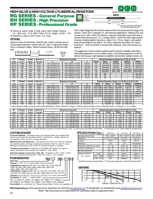
Internal construction of RP Series (non-inductive serpentine film)U U U U UU U U U UIndustry’s widest range of high value/ high voltage resistors- 1/8 ~ 20W, 1K Ω~ 1013Ω, 300V~ 90KV , TC’s to ±15ppm, ±0.05%~ 10% Available on T ape & Reel (sizes <2.5” long)RCD’s high voltage thick-film resistors represent the most advanced technology in the industry. Series RG is designed for semi-precision applications, offering a low cost solution up to 15KV . Series RH features a special composition and processing to achieve improved tolerance, TC, & voltage (60KV). Series RP utilize highest grade materials enabling tightest tolerances, lowest VC’s, TC’s to 15ppm, and superior power/temp/voltage levels (90KV). RP utilize serpentine film pattern for lowest inductance. Units are printed or banded with resistance value and tolerance as minimum.The ruggedness of these models enables superior long term reliability, especially in demanding applications such as military, space, and medical equipment, as well as electron microscopes, high impedance amplifiers, electrometer, radiation testers, etc.* Maximum working voltage is DC or AC RMS (50-60Hz sinusoidal) and is determined by E= (PR)1/2, E not to exceed value listed in column above. **Consult factory for res. values outside the standard rangeOPTIONSOptions include formed leads, matched sets, custom marking, burn-in,vacuum/space operation, custom sizes, etc. Opt. P = high pulse design,Opt.H= increased voltage, Opt.B=increased power, Opt.58=hermetic seal.* Extended temperature range available ** Tinned copper leads avail. on Series RP (specify Opt.25)DERA TING100 75 50 25 025 50 75 100 125 150 175 200 225AMBIENT TEMPERATURE (°C)% R A T E D P O W E RRPRG,RHIncreased Ratings - increased power and voltage ratings are available with special processing. By specifying Opt.H on RG series, voltage ratings are increased by 100% (by 50% on sizes 2W-4W).Matched Sets and Networks - cost savings up to 50% can often be achieved by specifying tight matching requirements instead of tight tol. and TC reqts.Resistance matching to 0.02% and TC tracking to 5ppm is available.Threaded Terminations - resistors are available with tapped end caps for series combination into virtually any voltage or resis. value.Hermetic-Sealed Construction (Opt. 58) - Available on RH1, RH2, & RH3for use in harshest environments. Add .08” to dia. & .18” to length.CUSTOM DESIGNS SPECIFICATIONS (Typ.)1RH2 is available in 400ppm TCR from 100G to 300G, 300G-600G is 1000ppm, 600G-3T is 1500ppm 2 RH3 is available in 400ppm TCR from 100G-600g, 600G-1T is 1000ppm, 1T-10T is 1500ppmG R W e g a t t a e g a tl o V c i r t c e l e i D ]m m [h c n I s n o i s n e m i D 01=K (**e g n a R e c n a ts i s e R d r a d n a t S 301=M ,601=G ,9)s e i r e S C °52@*g n i t a R h t g n e r t S L Dd m pp 52m p p 05mp p 001m p p 002m p p 0538/1G R W 8/1V 003V 005]0.1±4.3[40.±431.]46.0±7.1[520.±760.]5.[020.A /N M 01-M 1M 003-M 1M 003-M 1M 003-M 14/1G R W 4/1V 005V 005]0.1±5.6[40.±652.]46.0±5.2[520.±890.]6.[420.A /N M 05-K 001G 3-K 001G 3-K 001G 3-K 0012/1G R W 2/1V K 1V 005]0.1±4.9[40.±863.]18.0±4.3[230.±431.]46.[520.A /N M 05-K 001G 3-K 001G 3-K 001G 3-K 001S 1G R W 1V K 5.1V 005]3.1±0.21[50.±274.]18.0±0.4[230.±851.]7.[820.A /N M 05-k 002M 001-K 002M 003-K 002M 003-K 0021G R W 1V K 2V K 1]3.1±8.41[50.±185.]18.0±5.5[230.±612.}8.[130.A /N M 05-k 002M 001-K 002M 005-K 002M 005-K 0022G R W 2V K 5V K 1]6.1±9.62[260.±60.1]18.0±0.7[230.±572.}8.[130.A /N A /N ****G 5.1-M 13G R W 3V K 01V K 1]6.1±4.24[260.±76.1]18.0±0.7[230.±572.}8.[130.A /N A /N ****G 5.1-M 14G R W4VK 51VK 1]6.1±1.25[260.±50.2]20.1±5.8[230.±533.]1[040.A /N A /N ****G5.1-M 1P R W e g a t t a e g a t l o V c i r t c e l e i D ]m m [h c n I s n o i s n e m i D 01=K (**e g n a R e c n a t s i s e R d r a d n a t S 301=M ,601=G ,9)s e i r e S C °04@*g n i t a R h t g n e r t S L D d m p p 51m p p 52m p p 05m p p 001m p p 0024P R W 8.3V K 51V K 1]0.1±0.72[40.±360.1]46.±0.8[520.±513.]97.[130.G 1-K 1G 01-K 1G 01-K 1G 01-K 1G 01-K 15P R W 5V K 12V K 1]0.1±0.73[40.±754.1]46.±0.8[520.±513.]97.[130.G 1-K 1G 51-K 1G 51-K 1G 51-K 1G 51-K 18P R W 5.7V K 03V K 1]3.1±0.25[50.±740.2]46.±0.8[520.±513.]97.[130.G 1-K 1G 02-K 1G 02-K 1G 02-K 1G 02-K 101P R W 01V K 54V K 1]5.1±0.87[60.±170.3]46.±0.8[520.±513.]97.[130.G 1-K 1G 03-K 1G 03-K 1G 03-K 1G 03-K 11P R 4W 5.31V K 06V K 1]5.1±6.101[60.±000.4]46.±0.8[520.±513.]97.[130.G 1-K 1G 04-K 1G 04-K 1G 04-K 1G 04-K 161P R W 61V K 27V K 1]5.1±9.121[60.±008.4]46.±0.8[520.±513.]97.[130.G 1-K 1G 05-K 1G 05-K 1G 05-K 1G 05-K 102P R W 02V K 09V K 1]5.1±0.251[60.±489.5]46.±0.8[520.±513.]97.[130.G 1-K 1G 06-K 1G 06-K 1G 06-K 1G06-K 1s e i r e S G R s e i r e S H R s e i r e S P R e g n a R .p m e T g n i t a r e p O *C °551+o t 55-*C °551+o t 55-*C °522+o t 55-s e c n a r e l o T li a v a %1.0,%01-%1%5-%1.0%5-%50.0g n i t a o C y x o p E y x o p E e n o c i l i S ec n a t c ud n I w o L w o Le v i t c u d n I -n o N )V x 5.1e t n ,S 5,W x 5.1(d a o l r e v O %1±∆R %5.0±∆R %52.0±∆R )s r u o h 0001(ef i L d a o L %2±∆R %5.0±∆R %4.0±∆R e c n a t s i s e R e r u t s i o M %2±∆R %5.0±∆R %52.0±∆R tn e i c i f f e o C e g a t l o V G 1<ΩV /m p p 01-V /m p p 5-V /m p p 3.0-)V /m p p =C V (G 1ΩG 01-ΩV/m p p 03-V /m p p 02-V /m p p 5.1-T 7-G 01ΩA/N V/m p p 001-V/m p p 2-HR W e g a t t a e g a t l o V c i r t c e l e i D ]m m [h c n I s n o i s n e m i D 01=K (**e g n a R e c n a t s i s e R d r a d n a t S 301=M ,601=G ,901=T ,21)s e i r e S C °52@*g n i t a R h t g n e r t S L Ddm p p 52m p p 05m p p 001m p p 002≥m p p 0048/1H R W 8/1V 005V 005]0.1±1.6[40.±042.]6.0±61.2[520.±580.]6.[420.0M 05-K 001M 001-K 05M 001-K 01M 005-K 01G 4-M 0054/1H R W 4/1V 057V 005]0.1±0.9[40.±453.]0.1±00.3[40.±811.]6.[420.0M 001-K 001M 001-K 001M 003-K 01G 1-K 01G 5-G 12/1H R W 2/1V 0051V 005]0.1±7.21[40.±005.]0.1±75.4[40.±081.]8.[130.0M 001-K 001M 001-K 001G 1-K 001G 5-K 001G 5-G 11H R W 1V 0002V K 1]0.1±5.41[40.±175.]0.1±75.4[40.±081.]8.[130.0M 001-K 001M 005-K 001G 2-K 001G 51-K 001G 05-G 512H R W 2V 0005V K 1]0.2±4.52[80.±00.1]3.1±37.6[50.±562.]1/8.[40./130.M 001-K 001M 005-K 001G 2-K 001G 001-K 001T 3-G 00113H R W 3V K 01V K 1]0.2±9.14[80.±56.1]3.1±37.6[50.±562.]1/8.[40./130.M 001-K 001M 005-K 001G 2-K 001G 001-K 001T 01-G 00124H R W 4V K 51V K 1]0.2±1.25[80.±50.2]3.1±31.8[50.±023.]1/8.[40./130.-M 005-K 001G 2-K 001G 01-K 001-6H R W 6V K 02V K 1]0.2±77[80.±30.3]3.1±31.8[50.±023.]1/8.[40./130.-M 005-K 005G 2-K 005G 01-K 001-01H R W 01V K 53V K 1]1.3±4.911[21.±07.4]3.1±31.8[50.±023.]1/8.[40./130.-M 005-M 1G 2-M 1G 01-K 001-61H R W 61V K 06V K 1]1.3±091[21.±84.7]3.1±31.8[50.±023.]0.1[40.0-M 005-M 1G 2-M 1G 01-K 001-FA036C Sale of this product is in accordance with GF-061. Specifications subject to change without notice.RCD Components Inc, 520 E.Industrial Park Dr, Manchester, NH, USA 03109 Tel: 603-669-0054 Fax: 603-669-5455 Email:***********************RESISTORS CAPACITOR S C OILS DELAY LINESHIGH VALUE & HIGH VOLT AGE CYLINDRICAL RESISTORSRG SERIES - General Purpose RH SERIES - High PrecisionRP SERIES - Professional Grade69TC RCD Type1004=1M , Packaging Tolerance Options : P , Term.W is RoHS compliant & 260°C compatible。
RTR系列厚膜晶片电阻器规格标准书

F(±1%) E-24、E-96
10Ω≦R≦1MΩ
10Ω≦R≦1MΩ
100Ω≦R≦1MΩ -----
100Ω≦R≦1MΩ -----
100Ω≦R≦1MΩ -----
100Ω≦R≦1MΩ -----
100Ω≦R≦1MΩ -----
100Ω≦R≦1MΩ -----
100Ω≦R≦1MΩ -----55℃ ~ +155℃
Resistance to 下觀察焊錫面積。
(2).在電極邊緣處不應見到下層的物質
Soldering Heat
(例如白基板)。
抗焊錫熱
◎測試項目三(電烙鐵試驗): 加熱溫度:350±10℃ 電烙鐵加熱時間:3+1/-0 sec.
試驗項目三: (1).阻值變化率
取電鉻鐵加熱於電極兩端後,取出靜置60分鐘以上,再量測阻 △R%=±1.0%
-55℃ ~ +155℃
範圍
說明
周圍溫度若超過70℃至125℃之間,功率可照下 周圍溫度若超過70℃至155℃之間,功率可照下
圖曲線予以修定之。
圖曲線予以修定之。
負載功率比(%) 負載功率比(%)
70 100
功
80
率
衰
60
減
40
曲
125
線
20
圖
0
-55
20 40 60 80 100 120 140 160
RALEC
旺詮
RTR 系列厚膜晶片電阻器規格標準書
文件編號 版本日期
頁次
IE-SP-031 2019/07/02
1
1 適用範圍: 1.1 本規範適用於RTR系列無鉛、無鹵素符合RoHS條款的精密型厚膜晶片電阻器。 1.2 該產品應用於一般電子用途。
Vishay Draloric RCL e3 长端子终端厚膜片电阻器说明书

RCL12180000Z0EKRCL e3Vishay DraloricLong Side Termination Thick Film Chip ResistorsLINKS TO ADDITIONAL RESOURCESRCL e3 resistors series are the perfect choice for most fields of power measurement electronics where reliability, stability, power dissipation, and robust design is of major concern.Typical applications include power electronics in automotive and industrial appliances.FEATURES•Enhanced power rating •Long side terminations•Enhanced thermal cycling performance •AEC-Q200 qualified•Material categorization: for definitions of compliance please see /doc?99912APPLICATIONS•Automotive •Industrial •CommercialNotes(1)Please refer to APPLICATION INFORMATION below(2)Specified power rating requires dedicated mounting conditions to achieve the required thermal resistanceAPPLICATION INFORMATIONWhen the resistor dissipates power, a temperature rise above the ambient temperature occurs, dependent on the thermal resistance of the assembled resistor together with the printed circuit board. The rated dissipation applies only if the permitted film temperature is not exceeded.These resistors do not feature a limited lifetime when operated within the permissible limits. However, resistance value drift increasing over operating time may result in exceeding a limit acceptable to the specific application, thereby establishing afunctional lifetime.3D 3D3D ModelsTECHNICAL SPECIFICATIONSDESCRIPTION RCL0406 e3RCL0612 e3RCL1020 e3RCL1218 e3RCL1225 e3Imperial size 040606120612102012181225Metric size code RR1016MRR1632MRR1632MRR2550M RR3246M RR3263M Resistance range 1 Ω to 1 M Ω;jumper (0 Ω) 1 Ω to 39.2 k Ω;jumper (0 Ω)40.2 k Ω to 1 M Ω1 Ω to 1 M Ω;jumper (0 Ω)1 Ω to 2.2 M Ω;jumper (0 Ω)1 Ω to 1 M Ω;jumper (0 Ω)Resistance tolerance ± 5 %; ± 1 %Temperature coefficient ± 200 ppm/K; ± 100 ppm/K Rated dissipation, P 70 (1)0.25 W 1.0 W (2) 1.0 W (2) 1.0 W 1.0 W 2.0 W (2)Operating voltage, U max. AC RMS /DC 50 V200 V75 V200 V200 V200 VPermissible film temperature, ϑF max. (1)155 °C Operating temperature range -55 °C to +155 °CMax. resistance change at P 70 for resistance range, |ΔR /R | after:1000 h ≤ 1.0 %8000 h≤ 2.0 %Permissible voltage against ambient (insulation):1 min, U ins100 V100 V100 V300 V300 V300 VFailure rate: FIT observed≤ 0.1 x 10⁻⁹/hRCL e3Vishay DraloricNote•The temperature coefficient of resistance (TCR) is not specified for 0 Ω jumpersTEMPERATURE COEFFICIENT AND RESISTANCE RANGETYPE / SIZE TCR TOLERANCERESISTANCE E-SERIES RCL0406 e3± 200 ppm/K ± 5 % 1 Ω to 1 M ΩE24± 100 ppm/K ± 1 % 1 Ω to 1 M ΩE24; E96Jumper, I max. = 4 A ≤ 10 m Ω0 Ω-RCL0612 e3± 200 ppm/K ± 5 % 1 Ω to 1 M ΩE24± 100 ppm/K ± 1 % 1 Ω to 1 M ΩE24; E96Jumper, I max. = 6 A ≤ 10 m Ω0 Ω-RCL1020 e3± 200 ppm/K ± 5 % 1 Ω to 1 M ΩE24± 100 ppm/K ± 1 % 1 Ω to 1 M ΩE24; E96Jumper, I max. = 10 A≤ 10 m Ω0 Ω-RCL1218 e3± 200 ppm/K ± 5 % 1 Ω to 2.2 M ΩE24± 100 ppm/K ± 1 % 1 Ω to 2.2 M ΩE24; E96Jumper, I max. = 7 A ≤ 20 m Ω0 Ω-RCL1225 e3± 200 ppm/K ± 5 % 1 Ω to 1 M ΩE24± 100 ppm/K ± 1 % 1 Ω to 1 M ΩE24; E96Jumper, I max. = 12 A≤ 10 m Ω0 Ω-PACKAGINGTYPE / SIZE CODE QUANTITY PACKAGING STYLEWIDTHPITCH PACKAGING DIMENSIONS RCL0406 e3EA = ET15000Paper tape acc. to IEC 60286-3, Type 1a8 mm4 mmØ 180 mm/7"EB = ET510 000Ø 285 mm/11.25"EC = ET620 000Ø 330 mm/13"RCL0612 e3EA = ET15000 4 mm Ø 180 mm/7"EB = ET510 000Ø 285 mm/11.25"EC = ET620 000Ø 330 mm/13"RCL1020 e3EF = E024000Blister tape acc. to IEC 60286-3, Type 2a12 mm4 mmØ 180 mm/7"RCL1218 e3EK = ET94000RCL1225 e3EG = E6720008 mm EH = E8240004 mmPART NUMBER AND PRODUCT DESCRIPTIONPart Number: RCL061210K0FKEA Part Number: RCL06120000Z0EAMODEL RESISTANCE TOLERANCE TCR PACKAGINGRCL0406RCL0612RCL1020RCL1218RCL1225R = decimal K = thousand M = million 0000 = jumperF = ± 1 %J = ± 5 %Z = jumperK = ± 100 ppm/K N = ± 200 ppm/K 0 = jumperEA EB EC EF EG EH EKProduct Description: RCL0612 100 10K 1 % ET1 e3 Product Description: RCL0612 0R0 ET1 e3RCL061210010K1 %ET1e3MODEL TCR RESISTANCE TOLERANCE PACKAGING LEAD (Pb)-F REE RCL0406RCL0612RCL1020RCL1218RCL1225± 100 ppm/K ± 200 ppm/K10R = 10 Ω1K = 1 k Ω10K = 10 k Ω1M0 = 1 M Ω0R0 = jumper± 1 %± 5 %ET1ET5ET6ET9E02E67E82e3 = pure tin termination finishR C L 061210K 0F E AKRCL e3 Vishay DraloricDESCRIPTIONProduction is strictly controlled and follows an extensive set of instructions established for reproducibility. A cermet film layer and a glass-over are deposited on a high grade (Al2O3) ceramic substrate with its prepared inner contacts on both sides. A special laser is used to achieve the target value by smoothly fine trimming the resistive layer without damaging the ceramics. The resistor elements are covered by a protective coating designed for electrical, mechanical and climatic protection. The terminations receive a final pure tin on nickel plating.The result of the determined production is verified by an extensive testing procedure on 100 % of the individual chip resistors. Only accepted products are laid directly into the tape in accordance with IEC 60286-3 Type 1a and Type 2a (1).ASSEMBLYThe resistors are suitable for processing on automatic SMD assembly systems. They are suitable for automatic soldering using wave, reflow or vapor phase as shown in IEC 61760-1 (1). The encapsulation is resistant to all cleaning solvents commonly used in the electronics industry, including alcohols, esters and aqueous solutions. The suitability of conformal coatings, potting compounds and their processes, if applied, shall be qualified by appropriate means to ensure the long-term stability of the whole system.The resistors are RoHS-compliant, the pure tin plating provides compatibility with lead (Pb)-free and lead-containing soldering processes. Solderability is specified for 2 years after production or requalification. The permitted storage time is 20 years. The immunity of the plating against tin whisker growth has been proven under extensive testing.MATERIALSVishay acknowledges the following systems for the regulation of hazardous substances:•IEC 62474, Material Declaration for Products of and for the Electrotechnical Industry, with the list of declarable substances given therein (2)•The Global Automotive Declarable Substance List (GADSL) (3)•The REACH regulation (1907/2006/EC) and the related list of substances with very high concern (SVHC) (4) for its supply chain The products do not contain any of the banned substances as per IEC 62474, GADSL, or the SVHC list, see /how/leadfree.Hence the products fully comply with the following directives:•2000/53/EC End-of-Life Vehicle Directive (ELV) and Annex II (ELV II)•2011/65/EU Restriction of the Use of Hazardous Substances Directive (RoHS) with amendment 2015/863/EU•2012/19/EU Waste Electrical and Electronic Equipment Directive (WEEE)Vishay pursues the elimination of conflict minerals from its supply chain, see the Conflict Minerals Policy at /doc?49037.APPROVALSThe resistors are qualified according to AEC-Q200.Where applicable, the resistors are tested in accordance with EN 140401-802 which refers to EN 60115-1, EN 60115-8 and the variety of environmental test procedures of the IEC 60068 (1) series.RELATED PRODUCTSThe RCA-LS e3, Sulfur Resistant, Long Side Termination Thick F ilm Chip Resistors series is designed for harsh environment applications. For ordering RCA-LS e3 products please refer to latest edition of datasheet,/doc?20060.Notes(1)The quoted IEC standards are also released as EN standards with the same number and identical contents(2)The IEC 62474 list of declarable substances is maintained in a dedicated database, which is available at http://std.iec.ch/iec62474(3)The Global Automotive Declarable Substance List (GADSL) is maintained by the American Chemistry Council and available at (4)The SVHC list is maintained by the European Chemical Agency (ECHA) and available at http://echa.europa.eu/candidate-list-tableRCL e3Vishay DraloricFUNCTIONAL PERFORMANCESingle Pulse (1)Maximum pulse load, single pulse; applicable if and n < 1000 and ≤ max.;for permissible resistance change equivalent to 8000 h operationContinuous Pulse (1)Maximum pulse load, continuous pulses; applicable if ≤ P (ϑamb ) and ≤ max.;for permissible resistance change equivalent to 8000 h operationPulse Voltage (1)Maximum pulse voltage, single and continuous pulses; applicable if ≤ max.;for permissible resistance change equivalent to 8000 h operationNote(1)Pulse diagram under review to match upgraded rated dissipation and operating voltage0.010.111010010000.0000010.000010.00010.0010.010.1110100^P m a x .-P u l s e L o a d (W )t i -Pulse Duration (s)P 0→UˆU ˆ0.010.111010010000.0000010.000010.00010.0010.010.1110100^P m a x .-C o n t i n u o u s P u l s e L o a d (W )t i -Pulse Duration (s)P UˆU ˆ01002003004005006007008000.0000010.000010.00010.0010.010.1110^U m a x .-P u l s e V o l t a g e (V )t i -Pulse Duration (s)PˆP ˆRCL e3Vishay DraloricDerating0.51.01.52.02.5P -P o w e r D i s s i p a t i o n (W )ϑamb -Ambient Temperature (°C)RCL e3Vishay DraloricTESTS AND REQUIREMENTSAll executed tests are carried out in accordance with the following specifications:EN 60115-1, generic specification EN 60115-8 (successor of EN 140400), sectional specificationEN 140401-802, detail specification IEC 60068-2-xx, test methodsThe parameters stated in the Test Procedures and Requirements table are based on the required tests and permitted limits of EN 140401-802. The table presents only the most important tests, for the full test schedule refer to the documents listed above. However, some additional tests and a number of improvements against those minimum requirements have been included.The testing also covers most of the requirements specified by EIA/IS-703 and JIS-C-5201-1.The tests are carried out under standard atmospheric conditions in accordance with IEC 60068-1, 4.3, whereupon the following values are applied:Temperature: 15 °C to 35 °C Relative humidity: 25 % to 75 %Air pressure: 86 kPa to 106 kPa (860 mbar to 1060 mbar).TEST PROCEDURES AND REQUIREMENTSEN 60115-1 CLAUSE IEC60068-2 (1)TESTMETHODTESTPROCEDUREREQUIREMENTSPERMISSIBLE CHANGE (ΔR )Stability for product types:STABILITY CLASS 1OR BETTERSTABILITY CLASS 2OR BETTERRCL e31 Ω to 2.2 M Ω4.5-Resistance -± 1 %± 5 %4.8-Temperaturecoefficient(20 / -55 / 20) °C and (20 / 155 / 20) °C ± 100 ppm/K± 200 ppm/K4.25.1-Endurance at 70 °CU = or U = U max.;whichever is the less severe;1.5 h on; 0.5 h off70 °C; 1000 h ± (1 % R + 0.05 Ω)± (2 % R + 0.1 Ω)70 °C; 8000 h± (2 % R + 0.1 Ω)± (4 % R + 0.1 Ω)4.25.3-Endurance at upper category temperature 155 °C, 1000 h ± (1 % R + 0.05 Ω)± (2 % R + 0.1 Ω)4.2478 (Cab)Damp heat,steady state (40 ± 2) °C; 56 days;(93 ± 3) % RH;± (1 % R + 0.05 Ω)4.3767 (Cy)Damp heat,steady state,accelerated (85 ± 2) °C; (85 ± 5) % RH;U = ≤ 100 V;1000 h± (1 % R + 0.05 Ω)± (2 % R + 0.1 Ω)4.23-Climatic sequence:-± (1 % R + 0.05 Ω)± (2 % R + 0.1 Ω)4.23.2 2 (Bb)dry heat 125 °C; 16 h 4.23.330 (Db)damp heat, cyclic55 °C; 24 h; ≥ 90 % RH;1 cycle4.23.4 1 (Ab)cold -55 °C; 2 h4.23.513 (M)low air pressure 8.5 kPa; 2 h; (25 ± 10) °C4.23.630 (Db)damp heat, cyclic55 °C; 24 h;≥ 90 % RH; 5 cycles4.23.7-DC load U = ≤ U max.; 1 min- 1 (Aa)Cold -55 °C; 2 h ± (0.25 % R + 0.05 Ω)± (0.5 % R + 0.05 Ω)4.1914 (Na)Rapid change of temperature30 min at -55 °C and 30 min at 125 °C;1000 cycles± (1 % R + 0.05 Ω)P 70 x R 0.1 x P 85 x R P 70 x RRCL e3Vishay DraloricNote(1)The quoted IEC standards are also released as EN standards with the same number and identical contents4.13-Short time overloadU = 2.5 x ≤ 2 x U max.;whichever is the less severe;5 s ± (2 % R + 0.05 Ω)4.27-Single pulse high voltage overload Severity no. 4:U = 10 x orU = 2 x U max.;whichever is the less severe;10 pulses 10 μs/700 μs ± (1 % R + 0.05 Ω)no visible damage4.39-Periodic electricoverload U = orU = 2 x U max.;whichever is the less severe;0.1 s on; 2.5 s off;1000 cycles ± (1 % R + 0.05 Ω)no visible damage4.38-Electrostatic discharge(human body model)IEC 61340-3-1 (1);3 pos. + 3 neg. discharges;ESD voltage acc. to the size ± (1 % R + 0.05 Ω)4.22 6 (Fc)VibrationEndurance by sweeping;10 Hz to 2000 Hz;no resonance;amplitude ≤ 1.5 mm or≤ 200 m/s 2;7.5 h ± (0.25 % R + 0.05 Ω)no visible damage ± (0.5 % R + 0.05 Ω)no visible damage4.1758 (Td)SolderabilitySolder bath method;Sn60Pb40non-activated flux;(235 ± 5) °C;(2 ± 0.2) s Good tinning (≥ 95 % covered)no visible damageSolder bath method;Sn96.5Ag3Cu0.5non-activated flux;(245 ± 5) °C;(3 ± 0.3) s 4.1858 (Td)Resistance to soldering heat Solder bath method(260 ± 5) °C;(10 ± 1) s ± (0.25 % R + 0.05 Ω)± (0.5 % R + 0.05 Ω)4.2945 (XA)Component solventresistanceIsopropyl alcohol;+50 °C; method 2No visible damage 4.3221 (Uu 3)Shear (adhesion)17.7 N No visible damage4.3321 (Uu 1)Substrate bending Depth 2 mm;3 times ± (0.25 % R + 0.05 Ω)no visible damage, no open circuit in bent position4.7-Voltage proof U = 1.4 x U ins ; 60 s No flashover or breakdown 4.35-Flammability,needle flame testIEC 60695-11-5 (1);10 sNo burning after 30 sTEST PROCEDURES AND REQUIREMENTSEN 60115-1 CLAUSE IEC60068-2 (1)TESTMETHODTESTPROCEDUREREQUIREMENTSPERMISSIBLE CHANGE (ΔR )Stability for product types:STABILITY CLASS 1OR BETTERSTABILITY CLASS 2OR BETTERRCL e31 Ω to 2.2 M ΩP 70 x R P 70 x R 15 x P 70 x RRCL e3Vishay DraloricDIMENSIONSSOLDER PAD DIMENSIONSNotes•The given solder pad dimensions reflect the considerations for board design and assembly as outlined e.g in standards IEC 61188-5-x (1) orin publication IPC-7351.Still, the given solder pad dimensions will be found adequate for most general applications(1)The quoted IEC standards are also released as EN standards with the same number and identical contentsDIMENSIONS AND MASSTYPE / SIZE L (mm)W (mm)H (mm)T1(mm)T2(mm)MASS (mg)RCL0406 e3 1.0 ± 0.10 1.6 ± 0.100.35 ± 0.100.2 +0.10 / -0.150.2 ± 0.102RCL0612 e3 1.6 ± 0.20 3.2 ± 0.200.55 ± 0.100.35 ± 0.150.25 ± 0.1511RCL1020 e3 2.5 ± 0.20 5.0 ± 0.200.55 ± 0.100.38 ± 0.150.25 ± 0.1525.5RCL1218 e3 3.2 +0.10 / -0.20 4.6 ± 0.150.55 ± 0.050.45 ± 0.200.4 ± 0.2029.5RCL1225 e33.2 ± 0.206.3 ± 0.200.70 ± 0.100.8 ± 0.200.4 ± 0.2055RECOMMENDED SOLDER PAD DIMENSIONSTYPE / SIZE WAVE SOLDERINGREFLOW SOLDERING G (mm)Y (mm)X (mm)Z (mm)G (mm)Y (mm)X (mm)Z (mm)RCL0406 e30.300.80 1.95 1.900.350.60 1.75 1.55RCL0612 e30.50 1.20 3.70 2.900.60 1.00 3.50 2.60RCL1020 e3 1.30 1.25 5.50 3.80 1.30 1.10 5.25 3.50RCL1218 e3 1.80 1.30 5.10 4.40 1.90 1.10 4.90 4.10RCL1225 e31.101.806.804.701.201.606.604.40Legal Disclaimer Notice VishayDisclaimerALL PRODU CT, PRODU CT SPECIFICATIONS AND DATA ARE SU BJECT TO CHANGE WITHOU T NOTICE TO IMPROVE RELIABILITY, FUNCTION OR DESIGN OR OTHERWISE.Vishay Intertechnology, Inc., its affiliates, agents, and employees, and all persons acting on its or their behalf (collectively,“Vishay”), disclaim any and all liability for any errors, inaccuracies or incompleteness contained in any datasheet or in any other disclosure relating to any product.Vishay makes no warranty, representation or guarantee regarding the suitability of the products for any particular purpose or the continuing production of any product. To the maximum extent permitted by applicable law, Vishay disclaims (i) any and all liability arising out of the application or use of any product, (ii) any and all liability, including without limitation special, consequential or incidental damages, and (iii) any and all implied warranties, including warranties of fitness for particular purpose, non-infringement and merchantability.Statements regarding the suitability of products for certain types of applications are based on Vishay's knowledge of typical requirements that are often placed on Vishay products in generic applications. Such statements are not binding statements about the suitability of products for a particular application. It is the customer's responsibility to validate that a particular product with the properties described in the product specification is suitable for use in a particular application. Parameters provided in datasheets and / or specifications may vary in different applications and performance may vary over time. All operating parameters, including typical parameters, must be validated for each customer application by the customer's technical experts. Product specifications do not expand or otherwise modify Vishay's terms and conditions of purchase, including but not limited to the warranty expressed therein.Hyperlinks included in this datasheet may direct users to third-party websites. These links are provided as a convenience and for informational purposes only. Inclusion of these hyperlinks does not constitute an endorsement or an approval by Vishay of any of the products, services or opinions of the corporation, organization or individual associated with the third-party website. Vishay disclaims any and all liability and bears no responsibility for the accuracy, legality or content of the third-party website or for that of subsequent links.Except as expressly indicated in writing, Vishay products are not designed for use in medical, life-saving, or life-sustaining applications or for any other application in which the failure of the Vishay product could result in personal injury or death. Customers using or selling Vishay products not expressly indicated for use in such applications do so at their own risk. Please contact authorized Vishay personnel to obtain written terms and conditions regarding products designed for such applications. No license, express or implied, by estoppel or otherwise, to any intellectual property rights is granted by this document or by any conduct of Vishay. Product names and markings noted herein may be trademarks of their respective owners.© 2023 VISHAY INTERTECHNOLOGY, INC. ALL RIGHTS RESERVEDRCL12180000Z0EK。