
molex 5566规格图
ADuM3160_cn
GND2
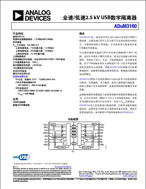
图1.
1
受美国专利5,952,849号、6,873,065号、7,075,329号和8,432,812号保护。 Document Feedback
Rev. C
Information furnished by Analog Devices is believed to be accurate and reliable. However, no responsibility is assumed by Analog Devices for its use, nor for any infringements of patents or other rights of third parties that may result from its use. Speci cations subject to change without notice. No license is granted by implication or otherwise under any patent or patent rights of Analog Devices. Trademarks and registered trademarks are the property of their respective owners.
概述
ADuM31601是一款采用 ADI公司 iCoupler®技术的 USB端口 隔离器,它将高速CMOS工艺与单片空芯变压器技术相结 合,可提供优异的工作性能,并且很容易与低速和全速 USB兼容外设集成。 许多微控制器实施的 USB 只向外部引脚提供 D+ 和 D− 线 路。这在许多情况下都符合需求,因为它仅需极少的外部 器件,并简化了设计;不过,当需要隔离时,这会带来难 题。由于USB线路必须在主动驱动D+/D−与允许外部电阻 设置总线状态之间切换,因此ADuM3160结构既可以检测 数据流向,也能够控制输出缓冲的状态。数据流向根据逐 包处理确定。 ADuM3160将基于边沿检测的 iCoupler技术与内部逻辑结 合使用,实现透明、易于配置、面对上游的端口隔离器。 隔离上游端口具有电路简单、电源管理和操作稳健等多种 优势。 这款隔离器的传播延迟与标准集线器和电缆的传播延迟相 当。它可以采用任一侧的4.5 V至5.5 V总线电压供电,并能 在内部将该电压调节至信号电平,从而与VBUSx直接相连。 ADuM3160对上拉电阻进行隔离控制,以便外设能控制连 接时序。该器件在空闲状态下消耗的电流非常低,因此不 需要挂起状态。也可提供5 kV强化隔离版本ADuM4160。
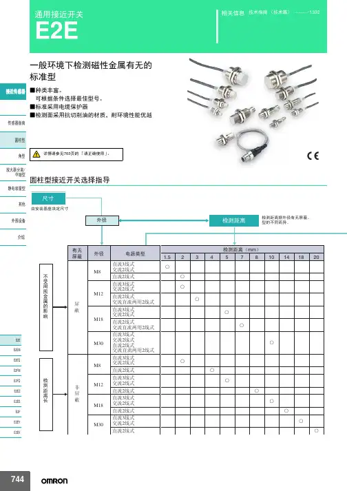
omron E2E通用接近开关 说明书
10mm 8mm
E2E-X10D1S-M1
D
——
—
E2E-X8MD1S-M1
D
——
—
M18
14mm
E2E-X14MD1S-M1
D
——
—
M30
20mm
E2E-X20MD1S-M1
D
——
—
M8
2mm
M12
ሣ㬑
M12 3mm
E2E-X2D1-M1G
A E2E-X2D2-M1G
D
E2E-X3D1-M1G *1
㾦ൟ
ᬒ఼ߚ行 Ё㒻ൟ
M30
10mm
无
M8
4mm
䴲ሣ㬑
M12
8mm
M18
14mm
E2E-X10D1-N E2E-X4MD1 E2E-X8MD1 E2E-X14MD1
*1*2*3 *2*3 *1*2*3 *1*2*3
E2E-X10D2-N E2E-X4MD2 E2E-X8MD2 E2E-X14MD2
ሣ㬑
1.5mm
E2E-X1R5E1-M3
M8 䴲ሣ㬑
M8 2mm
E2E-X2ME1-M3
输出形态PNP NO E2E-CR8B1 E2E-X1B1 E2E-C1B1 E2E-X1R5F1 E2E-X2F1 E2E-X5F1 E2E-X10F1 E2E-X2MF1 E2E-X5MF1 E2E-X10MF1 E2E-X18MF1
Ⳉ⌕2㒓ᓣ
ƻ ƻ
Ⳉ⌕3㒓ᓣ M18 Ѹ⌕2㒓ᓣ
Ⳉ⌕2㒓ᓣ
ƻ ƻ
Ⳉ⌕3㒓ᓣ M30 Ѹ⌕2㒓ᓣ
Ⳉ⌕2㒓ᓣ
ƻ ƻ
744
E2E
⬉⑤䕧ߎ Փ⫼⦃๗
黑金刚
铝电解电容器
小型铝电解电容器产品一览表
分类
高 小信 型赖 铝性 电 解 电特 容殊 器用
途
系列名
FL GPA GXE GXL LBG KZG LLA PH
特长·用途
小型尺寸长寿命品 125℃高温度小型化品 125℃高温度小型化品 125℃超长寿命 SRS安全气囊用 PC主板用 低漏电流品 闪光灯用
铝电解电容器
产品指南
接前页
标 准
小 型 ·
低
长 寿
高 信 形状
品
薄 型 化
Z化 命
赖 性
工作上限温度· 标准寿命 (hours)
额定电压范围 (Vdc)
04 105℃
3,000 6.3 ~ 50
04 125℃ 3,000/5,000 25 ~ 50
04 125℃ 2,000~5,000 10 ~ 450
小低长
型
·
寿
ห้องสมุดไป่ตู้
薄 型 化
Z化 命
高 信 形状 赖 性
工作上限温度· 标准寿命 (hours)
额定电压范围 (Vdc)
32 105℃
5,000 4 ~ 16
32 105℃
2,000 2.5 ~ 6.3
32 105℃
2,000 2.5 ~ 16
32 105℃ 1,000/2,000 2.5 ~ 25
04 105℃ 8,000/10,000 160 ~ 450
04 85℃
2,000 160 ~ 450
04 105℃
2,000 160 ~ 450
04 105℃
2,000 200 ~ 450
04 105℃
2,000 200、400
印制电路板设计要求-SMD元器件封装库尺寸要求
深圳市中兴通讯股份有限公司企业标准(技术标准)源自Q/ZX 04.100.5 -
2001
- 2001
印制电路板设计规范 ——SMD 元器件封装库尺寸要求
2001-12-11 发布
2002-01-01 实施
深圳市中兴通讯股份有限公司 发 布
Q/ZX 04.100.5 - 2001
目次
1 范围............................................................................. 1
6.1.6 SMD 排阻............................................................ 18
6.1.7 SOT 23.............................................................. 20
6.3.1 SOJ 元件尺寸........................................................ 50
6.3.2 SOJ 的焊盘尺寸...................................................... 51 6.4 四边有翼形引脚的元件.................................................... 54
6.1.15
SOT-323 元件(对应物料代码为 15100001)............................ 36
6.1.16
SOT-363 元件(对应物料代码为 15100001)............................ 38
PB系统闭环中文版

AC 电源规格
Type P
aP19
Type M
a P25
DC 电源规格
Type R 多轴
a P31
*脉冲控制时 按上位装置的脉冲输入指令进行工 作。
*I/O起动时 由I/O起动事先存储在驱动器内的位置指令或程序。
*串行通信起动时 由串行通信发送速度,加减速和移动量等数据进行控制。
*脉冲控制时 按上位装置的脉冲输入指令进行工作。
P/R
P/R
P/R
200
500
100
ɾɾɾɾɾɾɾɾɾɾɾ
800
1000
1600
2000
3200
4000
6400
5000
12800
10000 电子齿轮 16000
由于步进电机最大静止扭矩的特点,可实现稳定停止。 AC 电源输入型配有位置修正功能,不会因负荷变化造成错位。
可进行高分辨率的设定。而且,AC 系列配有电子齿轮比功能, 可配合装置进行灵活的分辨率设定。
RS-485,脉冲列共用(Type M) 500×4倍频=2000P/R PBM282FXE20 PBM284FXE20 PBM282FGAE20 PBM282FGBE20 PBM282FGEE20 PBM282FGGE20 PBM282FGJE20 PBM282FGLE20 PBM282FHLE20 PBM282FHME20 PBM282FCE20 PBM284FCE20 PBM423FXE20 PBM423FGAE20 PBM423FGBE20 PBM423FGEE20 PBM423FGGE20 PBM423FGJE20 PBM423FHJE20 PBM423FHLE20 PBM423FHME20 PBM423FCE20 PBM603FXE20 PBM604FXE20 PBM603FGAE20 PBM603FGBE20 PBM603FGEE20 PBM603FGGE20 PBM603FGJE20 PBM603FHLE20 PBM603FHME20 PBM603FCE20 PBM604FCE20
摩尔克斯 MLX 6.35mm 接头电源连接头文档说明书
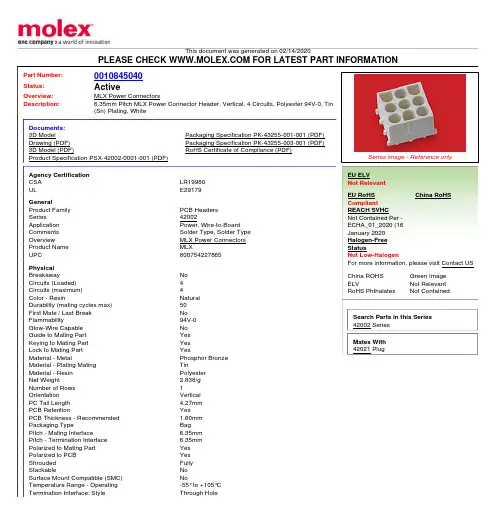
LR19980 E29179
PCB Headers 42002 Power, Wire-to-Board Solder Type, Solder Type MLX Power Connectors MLX 800754227865
No 4 4 Natural 50 No 94V-0 No Yes Yes Yes Phosphor Bronze Tin Polyester 2.838/g 1 Vertical 4.27mm Yes 1.60mm Bag 6.35mm 6.35mm Yes Yes Fully No No -55° to +105°C Through Hole
China ROHS ELV RoHS Phthalates
Green Image Not Relevant Not Contained
Search Parts in this Series 42002 Series
Mates With 42021 Plug
Electrical Current - Maximum per Contact Voltage - Maximum
Part Number:
Status:
Overview: Description:
This document was generated on 02/14/2020
PLEASE CHECK FOR LATEST PART INFORMATION
0010845040 Active
This document was generated on 02/14/2020
PLEASE CHECK FOR LATEST PART INFORMATION
Solder Process Data Duration at Max. Process Temperature (seconds) Lead-freeProcess Capability Process Temperature max. C
5634开发板硬件图(TRKMPC5634M)
VBAT
R14 1K C46 0.1 uF GND J3 2 3 21 1 3 20 15
RST INT
22 23
CT14 2
PCSB5
GND
C
J2 2
4.7K R37 15K RED LED D6
I/O-0 I/O-3 I/O-1 CS SCLK MOSI MISO U2A
AN18_SEL
GND Vsup 1 3
C40 220nF GND TP2 GND TP3 GND TP4 GND TP5 GND
AN15 C104 10nF GND
C103 10K
R41 C105 10K
VDD VDD VDD VDD
VSS VSS VSS VSS VSS VSS VSS VSS
MCU_RESETOUT MCU_RESET WKPCFG R28 BOOTCFG1 10K PLLRESheet 1 of 10
5
6
1
2
3
4
5
6
AN0_IN C90 AN1_IN AN2_IN P5V_MCU FB1 FERRITE BEAD D C26 10 uF GND + C27 10nF VDDA AN3_IN AN4_IN C96 10nF GND AN5_IN C98 10nF GND AN6_IN C84 10nF GND P5V 2 CT10 1 VRH_EN VRH FB3 FERRITE BEAD C61 10nF 1 GND CT11 2 VRL_EN FB4 FERRITE BEAD VRL C62 0.1 uF C48 0.1 uF REFBYPC AN7_IN C86 10nF GND AN9_IN C88 10nF GND AN11_IN C C34 10nF P5V R3 10k 1 1 P5V R29 10k GND AN12_IN P5V 2 P5V 3 C36 10nF GND WKPCFG AN13_IN C92 10nF GND P5V_MCU GND AN14_IN GND GND 10nF GND AN15_IN 10nF GND P5V_MCU AN16_IN C1 B 1nF GND P5V_MCU C5 1nF GND C6 0.1uF C7 1nF GND C8 0.1uF C2 0.1uF C3 1nF GND AN17_IN 10nF GND C4 0.1uF GND 10nF C94 1nF 1nF
mb202i,max202芯片资料datasheet
5 V DINROUTDOUT RS-232RIN RS-232120 kb/s15 kV HBMCopyright © 2016,Texas Instruments IncorporatedProduct FolderSample &BuyTechnical Documents Tools &SoftwareSupport &CommunityAn IMPORTANT NOTICE at the end of this data sheet addresses availability,warranty,changes,use in safety-critical applications,intellectual property matters and other important disclaimers.PRODUCTION DATA.MAX202SLLS576F –JULY 2003–REVISED SETPEMBER 2016MAX2025-V Dual RS-232Line Driver and Receiver With ±15-kV ESD Protection1Features•Meets or Exceeds the Requirements of TIA/EIA-232-F and ITU v.28Standards•ESD Protection for RS-232Bus Pins:±15-kV Human-Body Model•Operates at 5-V V CC Supply •Operates Up to 120kbit/s•Two Drivers and Two Receivers•Latch-Up Performance Exceeds 100mA Per JESD 78,Class II2Applications•Battery-Powered Systems •Notebooks •Laptops•Palmtop PCs•Hand-Held Equipment3DescriptionThe MAX202device consists of two line drivers,two line receivers,and a dual charge-pump circuit with ±15-kV ESD protection pin to pin (serial-port connection pins,including GND).The device meets the requirements of TIA/EIA-232-F and provides the electrical interface between an asynchronous communication controller and the serial-port connector.The charge pump and four small external capacitors allow operation from a single 5-V supply.The device operates at data signaling rates up to 120kbit/s and a maximum of 30-V/µs driver output slew rate.Device Information (1)PART NUMBER PACKAGE BODY SIZE (NOM)MAX202CD MAX202ID SOIC (16)9.90mm ×3.91mm MAX202CDW MAX202IDW SOIC WIDE (16)10.30mm ×7.50mm MAX202CPW MAX202IPWTSSOP (16)5.00mm x 4.40mm(1)For all available packages,see the orderable addendum atthe end of the data sheet.Block Diagram2MAX202SLLS576F –JULY 2003–REVISED SETPEMBER 2016Product Folder Links:MAX202Submit Documentation FeedbackCopyright ©2003–2016,Texas Instruments IncorporatedTable of Contents1Features ..................................................................12Applications ...........................................................13Description .............................................................14Revision History .....................................................25Pin Configuration and Functions . (36)Specifications .........................................................46.1Absolute Maximum Ratings......................................46.2ESD Ratings..............................................................46.3Recommended Operating Conditions.......................46.4Thermal Information..................................................46.5Electrical Characteristics...........................................56.6Switching Characteristics..........................................56.7Typical Characteristics .............................................67Parameter Measurement Information ..................78Detailed Description . (8)8.1Overview...................................................................88.2Functional Block Diagram.. (8)8.3Feature Description...................................................88.4Device Functional Modes (8)9Application and Implementation (10)9.1Application Information............................................109.2Typical Application.. (10)10Power Supply Recommendations .....................1311Layout . (13)11.1Layout Guidelines ................................................1311.2Layout Example. (13)12Device and Documentation Support (14)12.1Receiving Notification of Documentation Updates 1412.2Community Resources..........................................1412.3Trademarks...........................................................1412.4Electrostatic Discharge Caution............................1412.5Glossary................................................................1413Mechanical,Packaging,and OrderableInformation (14)4Revision HistoryNOTE:Page numbers for previous revisions may differ from page numbers in the current version.Changes from Revision E (April 2007)to Revision F Page•Added ESD Ratings table,Feature Description section,Device Functional Modes ,Application and Implementation section,Power Supply Recommendations section,Layout section,Device and Documentation Support section,andMechanical,Packaging,and Orderable Information section..................................................................................................1•Removed the Ordering Information table;see POA at the end of the data sheet .................................................................1•Changed values in the Thermal Information table to align with JEDEC standards (4)C1+ V CC V+ GND C1± DOUT1C2+ RIN1C2± ROUT1V ± DIN1DOUT2 DIN2RIN2ROUT23MAX202SLLS576F –JULY 2003–REVISED SETPEMBER 2016Product Folder Links:MAX202Submit Documentation FeedbackCopyright ©2003–2016,Texas Instruments Incorporated 5Pin Configuration and FunctionsD,DW,or PW Package 16-Pin SOIC or TSSOPTop ViewPin FunctionsPINI/O DESCRIPTION 1C1+—Positive lead of C1capacitor2V+O Positive charge pump output for storage capacitor only 3C1–—Negative lead of C1capacitor 4C2+—Positive lead of C2capacitor 5C2–—Negative lead of C2capacitor6V–O Negative charge pump output for storage capacitor only 7DOUT2O RS-232line data output (to remote RS-232system)8RIN2I RS-232line data input (from remote RS-232system)9ROUT2O Logic data output (to UART)10DIN2I Logic data input (from UART)11DIN1I Logic data input (from UART)12ROUT1O Logic data output (to UART)13RIN1I RS-232line data input (from remote RS-232system)14DOUT1O RS-232line data output (to remote RS-232system)15GND —Ground16V CC—Supply voltage,connect to external 5-V power supply4MAX202SLLS576F –JULY 2003–REVISED SETPEMBER 2016Product Folder Links:MAX202Submit Documentation FeedbackCopyright ©2003–2016,Texas Instruments Incorporated(1)Stresses beyond those listed under Absolute Maximum Ratings may cause permanent damage to the device.These are stress ratings only,which do not imply functional operation of the device at these or any other conditions beyond those indicated under Recommended Operating Conditions .Exposure to absolute-maximum-rated conditions for extended periods may affect device reliability.(2)All voltages are with respect to network GND.6Specifications6.1Absolute Maximum Ratingsover operating free-air temperature range (unless otherwise noted)(1)MINMAX UNIT Supply voltage,V CC (2)–0.36V Positive charge pump voltage,V+(2)V CC –0.314V Negative charge pump voltage,V–(2)–140.3V Input voltage,V I Drivers –0.3V++0.3V Receivers ±30Output voltage,V ODrivers V––0.3V++0.3VReceivers–0.3V CC +0.3Short-circuit duration,D OUTContinuousOperating junction temperature,T J 150°C Storage temperature,T stg –65150°C (1)JEDEC document JEP155states that 500-V HBM allows safe manufacturing with a standard ESD control process.(2)JEDEC document JEP157states that 250-V CDM allows safe manufacturing with a standard ESD control process.6.2ESD RatingsVALUEUNITV (ESD)Electrostatic dischargeHuman-body model (HBM),per ANSI/ESDA/JEDEC JS-001(1)Pins 7,8,13,and 14±15000V All other pins±2000Charged-device model (CDM),per JEDEC specification JESD22-C101(2)±1500(1)Test conditions are C1–C4=0.1µF at V CC =5V ±0.5V.6.3Recommended Operating Conditionsover operating free-air temperature range (unless otherwise noted (1);see Figure 10)MINNOMMAX UNIT Supply voltage4.555.5V V IH Driver high-level input voltage (D IN )2V V IL Driver low-level input voltage (D IN )0.8V V I Driver input voltage (D IN )0 5.5V Receiver input voltage –3030T A Operating free-air temperatureMAX202C 070°CMAX202I–4085(1)For more information about traditional and new thermal metrics,see the Semiconductor and IC Package Thermal Metrics application report.6.4Thermal InformationTHERMAL METRIC (1)MAX202UNITD (SOIC)DW (SOIC)PW (TSSOP)16PINS 16PINS 16PINS R θJA Junction-to-ambient thermal resistance 76.276.8101°C/W R θJC(top)Junction-to-case (top)thermal resistance 36.839.636.4°C/W R θJB Junction-to-board thermal resistance 33.941.545.9°C/W ψJT Junction-to-top characterization parameter 6.712.6 2.7°C/W ψJB Junction-to-board characterization parameter33.640.945.3°C/W5MAX202SLLS576F –JULY 2003–REVISED SETPEMBER 2016Product Folder Links:MAX202Submit Documentation FeedbackCopyright ©2003–2016,Texas Instruments Incorporated (1)Test conditions are C1–C4=0.1µF at V CC =5V ±0.5V.(2)All typical values are at V CC =5V,and T A =25°C.(3)Short-circuit durations should be controlled to prevent exceeding the device absolute power-dissipation ratings,and not more than one output should be shorted at a time.6.5Electrical Characteristicsover recommended ranges of supply voltage and operating free-air temperature (unless otherwise noted;see Figure 10)(1)PARAMETERTEST CONDITIONSMINTYP (2)MAX UNIT I CC Supply currentNo load,V CC =5V815mADRIVER SECTIONV OH High-level output voltage D OUT at R L =3k Ωto GND,D IN =GND 59V V OL Low-level output voltage D OUT at R L =3k Ωto GND,D IN =V CC –5–9V I IH High-level input current V I =V CC 0200µA I IL Low-level input current V I at 0V0–200µA I OS (3)Short-circuit output current V CC =5.5V,V O =0V±10±60mA r O Output resistance V CC ,V+,and V–=0V,V O =±2V 300ΩRECEIVER SECTIONV OH High-level output voltage I OH =–1mA 3.5V CC –0.4V V OL Low-level output voltageI OL =1.6mA 0.4V V IT+Positive-going input threshold voltage V CC =5V,T A =25°C 1.7 2.4V V IT–Negative-going input threshold voltage V CC =5V,T A =25°C0.8 1.2V V hys Input hysteresis (V IT+–V IT–)0.20.51V r i Input resistanceV I =±3V to ±25V357k Ω(1)Test conditions are C1–C4=0.1µF at V CC =5V ±0.5V.(2)All typical values are at V CC =5V,and T A =25°C.(3)Pulse skew is defined as |t PLH –t PHL |of each channel of the same device.6.6Switching Characteristicsover recommended ranges of suply voltage and operating free-air temperature (unless otherwise noted;see Figure 10)(1)PARAMETERTEST CONDITIONSMINTYP (2)MAXUNITDRIVER SECTIONMaximum data rateC L =50pF to 1000pF,R L =3k Ωto 7k ΩoneD OUT switching,see Figure 6120kbit/s t PLH(D)Propagation delay time,low-to high-level output C L =2500pF,R L =3k Ω,all drivers loaded,see Figure 62µs t PHL(D)Propagation delay time,high-to low-level output C L =2500pF,R L =3k Ω,all drivers loaded,see Figure 62µs t sk(p)Pulse skew (3)C L =150to 2500pF,R L =3k Ωto 7k Ω,see Figure 7300ns SR(tr)Slew rate,transition regionC L =50to 1000pF,R L =3k Ωto 7k Ω,V CC =5V,see Figure 63630V/µsRECEIVER SECTION (SEE Figure 8)t PLH(R)Propagation delay time,low-to high-level output C L =150pF 0.510µs t PHL(R)Propagation delay time,high-to low-level output C L =150pF 0.510µs t sk(p)Pulse skew (3)C L =150pF300ns6MAX202SLLS576F –JULY 2003–REVISED SETPEMBER 2016Product Folder Links:MAX202Submit Documentation FeedbackCopyright ©2003–2016,Texas Instruments Incorporated6.7Typical Characteristicsat T A =25°C (unless otherwise noted)TEST CIRCUITVOLTAGE WAVEFORMS50%50%–3 V3 V1.5 V1.5 VOutputInputV OL V OHt PHL (R)t PLH (R)OutputA)TEST CIRCUITVOLTAGE WAVEFORMS0 V 3 VOutputInputV OLV OHt PLH (D)t PHL (D)50%50%1.5 V1.5 VRS-232OutputA)TEST CIRCUITVOLTAGE WAVEFORMS0 V3 VOutputInputV OLV OH t PLH (D)RS-232Outputt PHL (D)A)1.5 V1.5 V3 V –3 V3 V –3 VSR(tf) =6 Vt or t PHL(D PLH(D))7MAX202SLLS576F –JULY 2003–REVISED SETPEMBER 2016Product Folder Links:MAX202Submit Documentation FeedbackCopyright ©2003–2016,Texas Instruments Incorporated 7Parameter Measurement InformationA.C L includes probe and jig capacitance.B.The pulse generator has the following characteristics:PRR =120kbit/s,Z O =50Ω,50%duty cycle,t r ≤10ns,t f ≤10ns.Figure 6.Driver Slew RateA.C L includes probe and jig capacitance.B.The pulse generator has the following characteristics:PRR =120kbit/s,Z O =50Ω,50%duty cycle,t r ≤10ns,t f ≤10ns.Figure 7.Driver Pulse SkewA.C L includes probe and jig capacitance.B.The pulse generator has the following characteristics:Z O =50Ω,50%duty cycle,t r ≤10ns,t f ≤10ns.Figure 8.Receiver Propagation Delay Times5 V DINROUTDOUT RS-232RIN RS-232120 kb/s15 kV HBMCopyright © 2016,Texas Instruments Incorporated8MAX202SLLS576F –JULY 2003–REVISED SETPEMBER 2016Product Folder Links:MAX202Submit Documentation FeedbackCopyright ©2003–2016,Texas Instruments Incorporated8Detailed Description8.1OverviewThe MAX202device is a dual driver and receiver that includes a capacitive voltage generator using four capacitors to supply TIA/EIA-232-F voltage levels from a single 5-V supply.Each receiver converts TIA/EIA-232-F inputs to 5-V TTL/CMOS levels.These receivers have shorted and open fail safe.The receiver can accept up to ±30-V inputs and decode inputs as low as ±3V.Each driver converts TTL/CMOS input levels into TIA/EIA-232-F levels.Outputs are protected against shorts to ground.8.2Functional Block Diagram8.3Feature Description8.3.1PowerThe power block increases and inverts the 5-V supply for the RS-232driver using a charge pump that requires four 0.1-µF external capacitors.8.3.2RS-232DriverTwo drivers interface standard logic levels to RS-232levels.The driver inputs do not have internal pullup resistors.Do not float the driver inputs.8.3.3RS-232ReceiverTwo Schmitt trigger receivers interface RS-232levels to standard logic levels.Each receiver has an internal 5-k Ωload to ground.An open input results in a high output on ROUT.8.4Device Functional Modes8.4.1V CC Powered by 5-VThe device is in normal operation when powered by 5V.8.4.2V CC UnpoweredWhen MAX202is unpowered,it can be safely connected to an active remote RS-232device.DIN1DOUT1RIN1ROUT1DIN2DOUT2RIN2ROUT29MAX202SLLS576F –JULY 2003–REVISED SETPEMBER 2016Product Folder Links:MAX202Submit Documentation FeedbackCopyright ©2003–2016,Texas Instruments Incorporated Device Functional Modes (continued)8.4.3Truth TablesTable 1and Table 2list the function for each driver and receiver (respectively).(1)H =high level,L =low levelTable 1.Function Table forEach Driver (1)INPUT DIN OUTPUT DOUTL H HL(1)H =high level,L =low level,Open =input disconnected or connected driver offTable 2.Function Table forEach Receiver (1)INPUT RIN OUTPUT ROUTL H H L OpenHFigure 9.Logic Diagram (Positive Logic)CBYPASS = 0.1F,m C10.1F,m 6.3 VCopyright © 2016,Texas Instruments Incorporated10MAX202SLLS576F –JULY 2003–REVISED SETPEMBER 2016Product Folder Links:MAX202Submit Documentation FeedbackCopyright ©2003–2016,Texas Instruments Incorporated9Application and ImplementationNOTEInformation in the following applications sections is not part of the TI component specification,and TI does not warrant its accuracy or completeness.TI’s customers are responsible for determining suitability of components for their purposes.Customers should validate and test their design implementation to confirm system functionality.9.1Application InformationFor proper operation,add capacitors as shown in Figure 10.Pins 9through 12connect to UART or general purpose logic lines.RS-232lines on pins 7,8,13,and 14connect to a connector or cable.9.2Typical ApplicationA.C3can be connected to V CC or GND.B.Resistor values shown are nominal.C.Nonpolarized ceramic capacitors are acceptable.If polarized tantalum or electrolytic capacitors are used,they must be connected as shown.Figure 10.Typical Operating Circuit and Capacitor Values9.2.1Design Requirements •V CC minimum is 4.5V and maximum is 5.5V.•Maximum recommended bit rate is 120kbps.RVHBM MAX202 SLLS576F–JULY2003–REVISED SETPEMBER2016 Typical Application(continued)9.2.2Detailed Design Procedure9.2.2.1Capacitor SelectionThe capacitor type used for C1through C4is not critical for proper operation.The MAX202requires0.1-µF capacitors.Capacitors up to10µF can be used without harm.Ceramic dielectrics are suggested for the0.1-µF capacitors.When using the minimum recommended capacitor values,make sure the capacitance value does not degrade excessively as the operating temperature varies.If in doubt,use capacitors with a larger(for example, 2×)nominal value.The capacitors'effective series resistance(ESR),which usually rises at low temperatures, influences the amount of ripple on V+and V–.Use larger capacitors(up to10µF)to reduce the output impedance at V+and V–.Bypass V CC to ground with at least0.1µF.In applications sensitive to power-supply noise generated by the charge pumps,decouple V CC to ground with a capacitor the same size as(or larger than)the charge-pump capacitors(C1to C4).9.2.2.2ESD ProtectionMAX202devices have standard ESD protection structures incorporated on all pins to protect against electrostatic discharges encountered during assembly and handling.In addition,the RS-232bus pins(driver outputs and receiver inputs)of these devices have an extra level of ESD protection.Advanced ESD structures were designed to successfully protect these bus pins against ESD discharge of±15-kV when powered down.9.2.2.3ESD Test ConditionsStringent ESD testing is performed by TI based on various conditions and procedures.Please contact TI for a reliability report that documents test setup,methodology,and results.9.2.2.4Human-Body Model(HBM)The HBM of ESD testing is shown in Figure11.Figure12shows the current waveform that is generated during a discharge into a low impedance.The model consists of a100-pF capacitor,charged to the ESD voltage of concern,and subsequently discharged into the device under test(DUT)through a1.5-kΩresistor.Figure11.HBM ESD Test Circuit1001502005001.51.00.50.0I -AD U T MAX202SLLS576F –JULY 2003–REVISED SETPEMBER Typical Application (continued)Figure 12.Typical HBM Current Waveform9.2.3Application Curve120kbit/s,1-nF loadFigure 13.Driver and Receiver Loopback SignalMAX202 SLLS576F–JULY2003–REVISED SETPEMBER201610Power Supply RecommendationsThe V CC voltage must be connected to the same power source used for logic device connected to DIN and ROUT pins.V CC must be between4.5V and5.5V.11Layout11.1Layout GuidelinesKeep the external capacitor traces short.This is more important on C1and C2nodes that have the fastest rise and fall times.For best ESD performance,make the impedance from MAX202ground pin to the ground plane of the circuit board as low as e wide metal and multiple vias on both sides of ground pin.11.2Layout ExampleFigure14.MAX202Circuit Board LayoutMAX202SLLS576F–JULY2003–REVISED 12Device and Documentation Support12.1Receiving Notification of Documentation UpdatesTo receive notification of documentation updates,navigate to the device product folder on .In the upper right corner,click on Alert me to register and receive a weekly digest of any product information that has changed.For change details,review the revision history included in any revised document.12.2Community ResourcesThe following links connect to TI community resources.Linked contents are provided"AS IS"by the respective contributors.They do not constitute TI specifications and do not necessarily reflect TI's views;see TI's Terms of Use.TI E2E™Online Community TI's Engineer-to-Engineer(E2E)Community.Created to foster collaboration among engineers.At ,you can ask questions,share knowledge,explore ideas and helpsolve problems with fellow engineers.Design Support TI's Design Support Quickly find helpful E2E forums along with design support tools and contact information for technical support.12.3TrademarksE2E is a trademark of Texas Instruments.All other trademarks are the property of their respective owners.12.4Electrostatic Discharge CautionThese devices have limited built-in ESD protection.The leads should be shorted together or the device placed in conductive foam during storage or handling to prevent electrostatic damage to the MOS gates.12.5GlossarySLYZ022—TI Glossary.This glossary lists and explains terms,acronyms,and definitions.13Mechanical,Packaging,and Orderable InformationThe following pages include mechanical,packaging,and orderable information.This information is the most current data available for the designated devices.This data is subject to change without notice and revision of this document.For browser-based versions of this data sheet,refer to the left-hand navigation.PACKAGING INFORMATIONAddendum-Page 1(1) The marketing status values are defined as follows:ACTIVE: Product device recommended for new designs.LIFEBUY: TI has announced that the device will be discontinued, and a lifetime-buy period is in effect.NRND: Not recommended for new designs. Device is in production to support existing customers, but TI does not recommend using this part in a new design.PREVIEW: Device has been announced but is not in production. Samples may or may not be available.OBSOLETE: TI has discontinued the production of the device.(2) Eco Plan - The planned eco-friendly classification: Pb-Free (RoHS), Pb-Free (RoHS Exempt), or Green (RoHS & no Sb/Br) - please check /productcontent for the latest availability information and additional product content details.TBD: The Pb-Free/Green conversion plan has not been defined.Pb-Free (RoHS): TI's terms "Lead-Free" or "Pb-Free" mean semiconductor products that are compatible with the current RoHS requirements for all 6 substances, including the requirement that lead not exceed 0.1% by weight in homogeneous materials. Where designed to be soldered at high temperatures, TI Pb-Free products are suitable for use in specified lead-free processes.Pb-Free (RoHS Exempt): This component has a RoHS exemption for either 1) lead-based flip-chip solder bumps used between the die and package, or 2) lead-based die adhesive used between the die and leadframe. The component is otherwise considered Pb-Free (RoHS compatible) as defined above.Green (RoHS & no Sb/Br): TI defines "Green" to mean Pb-Free (RoHS compatible), and free of Bromine (Br) and Antimony (Sb) based flame retardants (Br or Sb do not exceed 0.1% by weight in homogeneous material)(3) MSL, Peak Temp. - The Moisture Sensitivity Level rating according to the JEDEC industry standard classifications, and peak solder temperature.(4) There may be additional marking, which relates to the logo, the lot trace code information, or the environmental category on the device.Addendum-Page 2(5) Multiple Device Markings will be inside parentheses. Only one Device Marking contained in parentheses and separated by a "~" will appear on a device. If a line is indented then it is a continuation of the previous line and the two combined represent the entire Device Marking for that device.(6) Lead/Ball Finish - Orderable Devices may have multiple material finish options. Finish options are separated by a vertical ruled line. Lead/Ball Finish values may wrap to two lines if the finish value exceeds the maximum column width.Important Information and Disclaimer:The information provided on this page represents TI's knowledge and belief as of the date that it is provided. TI bases its knowledge and belief on information provided by third parties, and makes no representation or warranty as to the accuracy of such information. Efforts are underway to better integrate information from third parties. TI has taken and continues to take reasonable steps to provide representative and accurate information but may not have conducted destructive testing or chemical analysis on incoming materials and chemicals. TI and TI suppliers consider certain information to be proprietary, and thus CAS numbers and other limited information may not be available for release.In no event shall TI's liability arising out of such information exceed the total purchase price of the TI part(s) at issue in this document sold by TI to Customer on an annual basis.Addendum-Page 3TAPE AND REEL INFORMATION*All dimensions are nominal Device Package Type Package DrawingPinsSPQ Reel Diameter (mm)Reel Width W1(mm)A0(mm)B0(mm)K0(mm)P1(mm)W (mm)Pin1Quadrant MAX202CDR SOICD 162500330.016.4 6.510.3 2.18.016.0Q1MAX202CDWR SOICDW 162000330.016.410.7510.7 2.712.016.0Q1MAX202CPWR TSSOPPW 162000330.012.4 6.9 5.6 1.68.012.0Q1MAX202IDR SOICD 162500330.016.4 6.510.3 2.18.016.0Q1MAX202IDWR SOICDW 162000330.016.410.7510.7 2.712.016.0Q1MAX202IPWR TSSOP PW 162000330.012.4 6.9 5.6 1.68.012.0Q1*All dimensions are nominalDevice Package Type Package Drawing Pins SPQ Length(mm)Width(mm)Height(mm) MAX202CDR SOIC D162500333.2345.928.6 MAX202CDWR SOIC DW162000367.0367.038.0 MAX202CPWR TSSOP PW162000367.0367.035.0 MAX202IDR SOIC D162500333.2345.928.6 MAX202IDWR SOIC DW162000367.0367.038.0MAX202IPWR TSSOP PW162000367.0367.035.0IMPORTANT NOTICETexas Instruments Incorporated and its subsidiaries(TI)reserve the right to make corrections,enhancements,improvements and other changes to its semiconductor products and services per JESD46,latest issue,and to discontinue any product or service per JESD48,latest issue.Buyers should obtain the latest relevant information before placing orders and should verify that such information is current and complete.All semiconductor products(also referred to herein as“components”)are sold subject to TI’s terms and conditions of sale supplied at the time of order acknowledgment.TI warrants performance of its components to the specifications applicable at the time of sale,in accordance with the warranty in TI’s terms and conditions of sale of semiconductor products.Testing and other quality control techniques are used to the extent TI deems necessary to support this warranty.Except where mandated by applicable law,testing of all parameters of each component is not necessarily performed.TI assumes no liability for applications assistance or the design of Buyers’products.Buyers are responsible for their products and applications using TI components.To minimize the risks associated with Buyers’products and applications,Buyers should provide adequate design and operating safeguards.TI does not warrant or represent that any license,either express or implied,is granted under any patent right,copyright,mask work right,or other intellectual property right relating to any combination,machine,or process in which TI components or services are rmation published by TI regarding third-party products or services does not constitute a license to use such products or services or a warranty or endorsement e of such information may require a license from a third party under the patents or other intellectual property of the third party,or a license from TI under the patents or other intellectual property of TI.Reproduction of significant portions of TI information in TI data books or data sheets is permissible only if reproduction is without alteration and is accompanied by all associated warranties,conditions,limitations,and notices.TI is not responsible or liable for such altered rmation of third parties may be subject to additional restrictions.Resale of TI components or services with statements different from or beyond the parameters stated by TI for that component or service voids all express and any implied warranties for the associated TI component or service and is an unfair and deceptive business practice. TI is not responsible or liable for any such statements.Buyer acknowledges and agrees that it is solely responsible for compliance with all legal,regulatory and safety-related requirements concerning its products,and any use of TI components in its applications,notwithstanding any applications-related information or support that may be provided by TI.Buyer represents and agrees that it has all the necessary expertise to create and implement safeguards which anticipate dangerous consequences of failures,monitor failures and their consequences,lessen the likelihood of failures that might cause harm and take appropriate remedial actions.Buyer will fully indemnify TI and its representatives against any damages arising out of the use of any TI components in safety-critical applications.In some cases,TI components may be promoted specifically to facilitate safety-related applications.With such components,TI’s goal is to help enable customers to design and create their own end-product solutions that meet applicable functional safety standards and requirements.Nonetheless,such components are subject to these terms.No TI components are authorized for use in FDA Class III(or similar life-critical medical equipment)unless authorized officers of the parties have executed a special agreement specifically governing such use.Only those TI components which TI has specifically designated as military grade or“enhanced plastic”are designed and intended for use in military/aerospace applications or environments.Buyer acknowledges and agrees that any military or aerospace use of TI components which have not been so designated is solely at the Buyer's risk,and that Buyer is solely responsible for compliance with all legal and regulatory requirements in connection with such use.TI has specifically designated certain components as meeting ISO/TS16949requirements,mainly for automotive use.In any case of use of non-designated products,TI will not be responsible for any failure to meet ISO/TS16949.Products ApplicationsAudio /audio Automotive and Transportation /automotiveAmplifiers Communications and Telecom /communicationsData Converters Computers and Peripherals /computersDLP®Products Consumer Electronics /consumer-appsDSP Energy and Lighting /energyClocks and Timers /clocks Industrial /industrialInterface Medical /medicalLogic Security /securityPower Mgmt Space,Avionics and Defense /space-avionics-defense Microcontrollers Video and Imaging /videoRFID OMAP Applications Processors /omap TI E2E Community Wireless Connectivity /wirelessconnectivityMailing Address:Texas Instruments,Post Office Box655303,Dallas,Texas75265Copyright©2016,Texas Instruments Incorporated。
罗克韦尔-安全产品
存在感应式安全设备
典型接线图
安全光幕的典型接线图
安全边沿典型接线图
安全地毯典型接线图
安全互锁开关
优化生产的核心产品
舌片操作互锁开关
这些设备专用于滑动、铰链和提升防护门,可实 现防护门机器控制电路的电气互锁。操作这些设 备时需要实际接触执行器,防护门可立即打开。
保护闸互锁开关
这些设备专用于滑动、铰链和提升防护门,可实 现防护门机器控制电路的电气互锁。操作这些设 备时需要实际接触执行器,只有在该设备收到信 号防护门后才可以打开。这些设备非常适用于那 些需要防护门始终保持锁定直到潜在危险已停止 并达成安全条件的应用。
近似尺寸-mm(英寸) 以下尺寸不适合用作安装尺寸
注:TLA-1 GD2, TLS-2 GD2, TLS-3 GD2 互锁开关 安装尺寸图
安全继电器
优化生产的核心产品
安全继电器-可选延时输出
这些设备被设计用于检测与安全电路有关的故障,例 如传感器、接线、接触器等的故障,以及作为中间继 电器提供有保证的开关动作。对于各种输入和输出而 言,包括中间动作输出以及延时动作输出,有多种版 本可以适用。这些单元非常适用于像互锁、急停开 关、光幕和安全地毯等这样的安全设备。
•
•
•
•
•
•
立即输出
延时输出
电压
重置
输出开关
[A]
安全
辅助
安全
辅助 时间 24V AC/DC 115V AC 230V AC 24V DC 自动/ 监控
(EM) (SS) (EM) (SS) (SS) (EM) (EM) (SS) (EM) (SS) 延时 产品目录号 产品目录号 产品目录号 产品目录号 手动 手动 250V 24V
电磁兼容(EMC)设计参考电路
1000pF/2KV FBMA-11-160808-601A10T
1 2 3.3V-Earth
L5
1000pF
C5
C6
1000pF
C1 1000pF
L3
C4 100nF
C3
100nF
C13 1000pF/2KV C14 1000pF/2KV
A
备注: 1、C2、C9、C10、C11 为预设计,根据实际的情况增加,一般不需要增加; 2、C13、C14为预设计,根据实际的情况增加或调整; 3.如防雷等级需要打空接(4、5、7、8)pin,可接上D5做防护。 4.此方案相比中心抽头的方案有了明显的差摸保护。如果要测试绝缘阻抗,请与工程师确认具体的方案。 5.如果4、5、7、8 PIN 不需要测试的话,这部分的器件可以不加
5
3
2
1
千兆网口EMC设计标准电路
D
C1 100nF
1 TCT1 TD1+ TD1-
U1
MCT1 MX1+ MX124 23 22 MX1+ MX1MX1+ MX1MX2+ MX3+ MX3MX2MX4+ MX41 2 3 4 5 6 7 8 MX1+ MX1MX2+ MX3+ MX3MX2MX4+ MX49
MCT3 MX3+ MX3-
18 17 16 MX3+ MX3-
TVS3
BV03C
330R R5 link_o
C4 100nF
10 11 12
TCT4 TD4+ TD4-
MCT4 MX4+ MX4-
15 14 13 MX4+ MX4-