LC185EXE-TEA1屏规格书
MEMORY存储芯片MT48LC8M16A2TG-6A IT L中文规格书
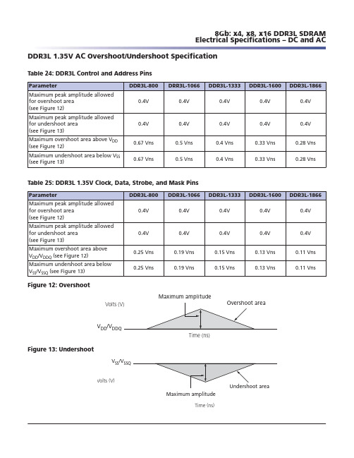
Parameter
Maximum peak amplitude allowed for overshoot area (see Figure 12)
Maximum peak amplitude allowed for undershoot area (see Figure 13)
Maximum overshoot area above VDD (see Figure 12)
ACTIVATE to internal READ or WRITE delay time
PRECHARGE command period
ACTIVATE-to-ACTIVATE or REFRESH command period
ACTIVATE-to-PRECHARGE command period
4
ns
3
ns
4
ns
4
ns
3
ns
4
ns
3
ns
4
ns
4
ns
3
ns
4
ns
4
ns
4
ns
4
ns
3
CK
CK
Notes:
1. The -107 speed grade is backward compatible with 1600, CL = 11 (-125) , 1333, CL = 9 (-15E) and 1066, CL = 7 (-187E).
4. Reserved settings are not allowed.
8Gb: x4, x8, x16 DDR3L SDRAM Electrical Specifications – DC and AC
BenQ 18.5 宽屏 液晶显示器 用戶手冊
18.5"宽屏 液晶显示器用戶手冊预防措施入门第一层第三层按键启动。
按其它4个的任一按键启动菜单。
按在OSD的跳出窗口上的对应的功能图标按键。
第二层定制您的显示器重要:屏幕显示(OSD)系统提供了全套的可定制工具来优化您的显示器。
重要:此外,我们也准备了其它比较简单的方法去改变不同的显示模式,有4种模式,包含:一般,电影,写真,游戏。
虽然您可以执行丰富的自定义,但我们还是强烈建议您使用“自动调整”功能。
它使用默认值来优化显示器的性能。
激活OSD 选择右边的第二个按钮“自动调整”功能。
疑难解答现象 检查项目1.下列频率范围是工作周期。
如果所选的模式处于下列周期范围内,但不符合所支持的时脉频率,那就不能保证最佳的显示性能。
如果所选的模式超出了工作周期,那么屏幕就会变成空白(只显示“Input Not Supported ”(只显示不支持的输入),然后进入省电模式。
2.模式判断基本上与同步极性无关,除非两个以上的模式都属于所支持的时脉列表,并且只能通过同步极性来加以判断。
3.同时,并不需要为所支持的时脉输入确切的频率。
4.可以对VGA 卡的偏差进行校正。
5.横向频率6.纵向频率机能规格与特性接口频率30 ~ 83KHz 50 ~ 76Hz1 640x350 25.18 31.47 70.092 640x480 25.17 31.47 59.94 3640x480 31.5 37.5 754720x400 28.32 31.47 70.085 832x624 57.27 49.71 74.53 6800x600 40 37.88 60.327800x600 49.5 46.88 7581024x768 65 48.36 60 9 1024x768 80 60.24 74.93 101024x768 78.75 60.02 75.03 11 1152x720 66.75 44.86 60 12 1280x720 74.25 45 59.94 131280x720 74.5 44.77 59.86141280x720 95.75 56.46 74.7815 1280x768-R 68.25 47.4 6016 1280x768 79.5 47.78 59.87 17 1360x768 85.5 47.71 60.01 18 1366x768 85.5 47.71 59.79输入预设型号输入预设型号 编号分辨率像素时钟 (MHz)水平同步 (KHz) 垂直同步 (Hz)。
ELAN EM78F811N 8位微控制器 产品规格书说明书
产品规格书版本1.5义隆电子股份有限公司2021.07商标告之:IBM 为一个注册商标,PS/2是IBM 的商标之一。
Windows 是微软公司的商标。
ELAN 和ELAN 标志是义隆电子股份有限公司的商标。
版权所有 © 2021义隆电子股份有限公司所有权利保留台湾印制本规格书内容如有变动恕不另作通知。
关于该规格书的准确性、适当性或者完整性,义隆电子股份有限公司不承担任何责任。
义隆电子股份有限公司不承诺对本规格书之内容及信息有更新及校正之义务。
本规格书的内容及信息将为符合确认之指示而变更。
在任何情况下,义隆电子股份有限公司对本规格书中的信息或内容的错误、遗漏,或者其它不准确性不承担任何责任。
由于使用本规格书中的信息或内容而导致的直接,间接,特别附随的或结果的损害,义隆电子股份有限公司没有义务负责。
本规格书中提到的软件(如果有),都是依据授权或保密合约所合法提供的,并且只能在这些合约的许可条件下使用或者复制。
义隆电子股份有限公司的产品不是专门设计来应用于生命维持的用具,装置或者系统。
义隆电子股份有限公司的产品不支持而且禁止在这些方面的应用。
未经义隆电子股份有限公司书面同意,任何个人或公司不得以任何形式或方式对本规格书的内容之任一部分进行复制或传输。
义隆电子股份有限公司 总公司:地址: 30076新竹科学工业园区创新一路12号电话: +886 3 563-9977 传真: +886 3 563-9966 *****************.tw http :// 香港分公司:义隆电子(香港)股份有限公司 地址:九龙观塘巧明街95号世达 中心19楼A 室电话: +852 2723-3376 传真: +852 2723-7780美国:Elan InformationTechnology Group (U.S.A.) 地址: 10268 Bandley Drive Suite 101 , Cupertino , CA 95014,USA 电话: +1 408 366-8225 传真: +1 408 366-8225深圳分公司:义隆电子(深圳)有限公司地址:518057深圳市南山区高新技术产业园南区高新南六道迈科龙大厦8A电话: +86 755 2601-0565 传真: +86 755 2601-0500 ******************.cn上海分公司:义隆电子(上海)有限公司地址:上海市浦东新区盛荣路88弄3号703室(盛大天地源创谷内)电话:+86 21 5080-3866 ******************.cn目录目录1 综述 (1)2 特性 (1)3 引脚配置 (2)3.1 10-Pin MSOP (2)3.2 16-Pin DIP/SOP (2)3.3 14-Pin SOP (2)4 引脚描述 (3)5 系统概述 (5)5.1 内存图 (5)5.2 模块图 (6)6 功能描述 (7)6.1 操作寄存器 (7)6.1.1 R0:IAR (间接寻址寄存器) (7)6.1.2 R1 :TCC(定时器时钟) (7)6.1.3 R2:PC (程序计数器和堆栈) (7)6.1.4 R3 :SR(状态寄存器) (10)6.1.5 R4 :RSR(RAM选择寄存器) (10)6.1.6 Bank 0 R5 ~ R6, R8 (Port 5 ~ Port 6, Port 8) (10)6.1.7 Bank 0 R9:TBLP (指令TBRD表指针寄存器) (11)6.1.8 Bank 0 RA:WUPC (唤醒控制寄存器) (11)6.1.9 Bank 0 RB:EECR (EEPROM控制寄存器) (12)6.1.10 Bank 0 RC: EEPA (128 字节 EEPROM 地址) (12)6.1.11 Bank 0 RD: EEPD (128字节EEPROM 数据) (12)6.1.12 Bank 0 RE: OMCR (模式选择寄存器) (12)6.1.13 Bank 0 RF: ISR1 (中断状态寄存器 1) (15)6.1.14 R10 ~ R3F (15)6.1.15 Bank 1 R5~R7 (16)6.1.16 Bank 1 R8 (IRC 选择寄存器) (16)6.1.17 Bank 1 R9: TM1CR1 (定时器/计数器 1控制寄存器1) (16)6.1.18 Bank 1 RA: TM1CR2(定时器/计数器 1控制寄存器 2) (17)6.1.19 Bank 1 RB: TM1DAH (定时器/计数器 1数据缓冲A高字节) (18)6.1.20 Bank 1 RC: TM1DAL (定时器/计数器 1数据缓冲A低字节) (18)6.1.21 Bank 1 RD: TM1DBH (定时器/计数器 1数据缓冲B高字节) (18)6.1.22 Bank 1 RE: TM1DBL (定时器/计数器 1数据缓冲B低字节) (18)6.1.23 Bank 1 RF: ISR2 (中断状态寄存器 2) (19)6.1.24 Bank 2 R5:AISR (ADC输入选择寄存器) (19)6.1.25 Bank 2 R6: ADCON (A/D控制寄存器) (20)6.1.26 Bank 2 R7: ADCON2 (A/D控制寄存器2) (21)6.1.27 Bank 2 R8 : ADDH (AD高 8位数据缓存) (22)6.1.28 Bank 2 R9 : ADDL (AD低4位数据缓存) (22)6.1.29 Bank 2 RA: URCR (UART控制寄存器) (22)6.1.30 Bank 2 RB: URS (UART 状态寄存器) (23)6.1.31 Bank 2 RC: URTD (UART 发送数据缓冲寄存器) (24)6.1.32 Bank 2 RD: URRDL (UART 接收数据低位缓冲寄存器) (24)目录6.1.33 Bank 2 RE: URRDH (UART 接收数据高位缓冲寄存器) (24)6.1.34 Bank 2 RF (24)6.1.35 Bank 3 R5 (24)6.1.36 Bank 3 R6 : TBHP(指令TBRD的表指针寄存器) (24)6.1.37 Bank 3 R7: CMP2CON(比较器2控制寄存器) (25)6.1.38 Bank 3 R8 ~ RC (25)6.1.39 Bank 3 RD :TC3CR (定时器3控制) (25)6.1.40 Bank 3 RE :TC3D (定时器 3 数据缓存) (27)6.1.41 Bank 3 RF (27)6.2 特殊功能寄存器 (28)6.2.1 A (累加器) (28)6.2.2 CONT (控制寄存器) (28)6.2.3 IOC5 ~ IOC6, IOC8 (I/O端口控制寄存器) (28)6.2.4 IOC7, IOC9 (28)6.2.5 IOCA:WDTCR (WDT 控制寄存器) (29)6.2.6 IOCB: P6PDCR (下拉控制寄存器2) (29)6.2.7 IOCC: P6ODCR (漏极开路控制寄存器) (30)6.2.8 IOCD: P9PHCR (上拉控制寄存器2) (30)6.2.9 IOCE:IMR2 (中断屏蔽寄存器2) (31)6.2.10 IOCF: IMR1(中断屏蔽寄存器1) (31)6.3 TCC/WDT 与预分频器 (33)6.4 I/O 端口 (34)6.4.1 使用端口6输入状态改变唤醒/中断功能 (36)6.5 复位和唤醒 (37)6.5.1 复位 (37)6.5.2 总结唤醒和中断模式操作 (39)6.5.3 寄存器初始值的总结 (42)6.5.4 状态寄存器的T和P状态 (49)6.6 中断 (50)6.7 数据EEPROM (52)6.7.1 数据EEPROM控制寄存器 (52)6.7.2 编程步骤 / 举例示范 (52)6.8 模拟数字转换器(ADC) (53)6.8.1 A/D 取样时间 (53)6.8.2 A/D 转换时间 (54)6.8.3 睡眠期间的A/D转换 (54)6.8.4 编程步骤/注意事项 (55)6.9 定时器/计数器1 (TM1) (58)6.9.1 定时器/计数器模式 (58)6.9.2 窗口模式 (59)6.9.3 捕捉模式 (60)6.9.4 可编程分频输出模式和脉冲宽度调制模式 (62)6.9.5 蜂鸣器 (63)6.10 定时器/计数器3 (63)6.11 UART (65)6.11.1 UART 模式 (66)6.11.2 发送 (67)目录6.11.3 接收 (67)6.11.4 波特率发生器 (68)6.11 .5 UART 时序 (68)6.12 比较器 (69)6.12.1 外部参考信号 (69)6.12.2 内部参考电压 (70)6.12.3 比较器输出 (70)6.12.4 中断 (70)6.12.5 从睡眠至唤醒 (70)6.12.6 比较器初始化步骤 (71)6.13 振荡器 (71)6.13.1 振荡模式 (71)6.13.2 晶振 / 陶瓷谐振器(晶体) (72)6.13.3 外部RC振荡模式 (73)6.13.4 内部 RC 振荡模式 (74)6.14 代码选项寄存器 (75)6.14.1 代码选项寄存器 (Word 0) (75)6.14.2 代码选项寄存器(Word 1) (77)6.14.3 客户ID寄存器(Word 2) (78)6.15 上电注意事项 (79)6.16 外部上电复位电路 (79)6.17 残留电压保护 (80)6.18 指令集 (81)7片上调试系统(OCDS) (84)7.1 片上调试的限制 (84)8 时序图 (85)9 绝对最大额定参数 (86)10 DC电气特性 (87)11 AC电气特性 (92)A 编码与制造信息 (93)B 封装类型 (94)C 封装结构 (95)C.1 EM78F811NMS10 (95)C.2 EM78F811NSO14 (96)C.3 EM78F811NAD16 (97)C.4 EM78F811NASO16A (98)D 品质保证和可靠性 (99)D.1 地址缺陷检测 (99)目录规格修订历史目录用户应用注意事项(使用此IC前,应注意如下描述的注意事项,它包含重要信息)1. 如果IRC频率从A频率变为B频率,MCU需要等待一些时间才可以工作。
雅特力 AT32F415系列 数据手册说明书

基于ARM®32位的Cortex®-M4微控制器,带64 K字节至256 K字节闪存、sLib、USB OTG、11个定时器、1个ADC、2个比较器、12个通信接口功能⏹内核:ARM®32位的Cortex®-M4 CPU−最高150 MHz工作频率,带存储器保护单元(MPU),内建单周期乘法和硬件除法−具有DSP指令集⏹存储器−从64 K字节至256 K字节的闪存程序/数据存储器− 18 K字节的系统存储器可作启动加载程序(Bootloader)用外,也可一次性配置成一般用户程序和数据区− 32 K字节的SRAM− sLib:将指定之主存储区设为执行代码安全库区,此区代码仅能调用无法读取⏹时钟、复位和电源管理− 2.6至3.6伏供电和I/O引脚−上电/断电复位(POR/PDR)、可编程电压监测器(PVD)− 4至25 MHz晶体振荡器−内嵌经出厂调校的48 MHz RC振荡器(25 °C达1 %精度,-40 °C至+105 °C达2.5 %精度),带自动时钟校准功能(ACC)−内嵌带校准的40 kHz RC振荡器−带校准功能的32 kHz晶体振荡器⏹低功耗−睡眠、停机、和待机模式− V BAT为ERTC和20个32位的后备寄存器供电⏹1个12位A/D转换器,0.5 μs转换时间(多达16个输入通道)−转换范围:0至3.6 V−一组采样和保持功能−温度传感器⏹2个比较器⏹DMA:14通道DMA控制器−支持的外设:定时器、ADC、SDIO、I2S、SPI、I2C、和USART⏹调试模式−串行线调试(SWD)和JTAG接口⏹多达55个快速I/O端口− 27/39/55个多功能双向的I/O口,所有I/O口可以映像到16个外部中断;几乎所有I/O口可容忍5V输入信号−所有I/O口均为快速I/O,寄存器存取速度最高f AHB/2⏹多达11个定时器−多达5个16位定时器+2个32位定时器,每个定时器有多达4个用于输入捕获/输出比较/PWM或脉冲计数的通道和增量编码器输入− 1个16位带死区控制和紧急刹车,用于电机控制的PWM高级控制定时器− 2个看门狗定时器(独立的和窗口型的)−系统时间定时器:24位自减型计数器⏹ERTC:增强型RTC,具亚秒级精度及硬件日历⏹多达12个通信接口− 2个I2C接口(支持SMBus/PMBus)−多达5个USART接口(支持ISO7816,LIN,IrDA接口和调制解调控制)− 2个SPI接口(50M位/秒),2个均可复用为I2S接口− CAN接口(2.0B主动),内置256字节的专用SRAM− USB 2.0全速设备/主机/OTG控制器,内置1280字节的专用SRAM,设备模式时支持无晶振(Crystal-less)− SDIO接口⏹CRC计算单元⏹96位的芯片唯一代码⏹封装− LQFP64 10 x 10 mm− LQFP64 7 x 7 mm− LQFP48 7 x 7 mm− QFN48 6 x 6 mm− QFN32 4 x 4 mm目录1介绍 (9)2规格说明 (10)2.1器件一览 (11)2.2概述 (12)2.2.1ARM®Cortex®-M4,配有DSP指令 (12)2.2.2存储器保护单元(MPU) (14)2.2.3闪存存储器 (14)2.2.4循环冗余校验(CRC)计算单元 (14)2.2.5内置SRAM (14)2.2.6嵌套的向量式中断控制器(NVIC) (14)2.2.7外部中断/事件控制器(EXTI) (15)2.2.8时钟和启动 (15)2.2.9启动模式 (17)2.2.10供电方案 (17)2.2.11供电监控器 (17)2.2.12电压调压器 (17)2.2.13低功耗模式 (18)2.2.14直接存储器访问控制器(DMA) (18)2.2.15增强型实时时钟(ERTC)和后备份寄存器 (18)2.2.16定时器和看门狗 (19)2.2.17内部集成电路总线(I2C) (21)2.2.18通用同步/异步收发器(USART) (21)2.2.19串行外设接口(SPI) (21)2.2.20内部集成音频接口(I2S) (21)2.2.21安全数字输入/输出接口(SDIO) (21)2.2.22控制器区域网络(CAN) (21)2.2.23通用串行总线OTG全速(USB OTG FS) (22)2.2.24通用输入输出口(GPIO) (22)2.2.26模拟/数字转换器(ADC) (22)2.2.27温度传感器 (22)2.2.28比较器(COMP) (23)2.2.29串行线JTAG调试口(SWJ-DP) (23)3引脚定义 (24)4存储器映像 (30)5电气特性 (31)5.1测试条件 (31)5.1.1最小和最大数值 (31)5.1.2典型数值 (31)5.1.3典型曲线 (31)5.1.4负载电容 (31)5.1.5引脚输入电压 (31)5.1.6供电方案 (32)5.1.7电流消耗测量 (32)5.2绝对最大额定值 (33)5.3工作条件 (34)5.3.1通用工作条件 (34)5.3.2上电和掉电时的工作条件 (34)5.3.3内嵌复位和电源控制模块特性 (35)5.3.4内置的参照电压 (36)5.3.5供电电流特性 (36)5.3.6外部时钟源特性 (44)5.3.7内部时钟源特性 (48)5.3.8PLL特性 (50)5.3.9存储器特性 (50)5.3.10EMC特性 (51)5.3.11绝对最大值(电气敏感性) (52)5.3.13NRST引脚特性 (55)5.3.14TMR定时器特性 (55)5.3.15通信接口 (56)5.3.16CAN(控制器局域网络)接口 (64)5.3.1712位ADC特性 (64)5.3.18比较器特性 (68)5.3.19温度传感器特性 (69)6封装特性 (70)6.1LQFP64 – 10 x 10 mm封装数据 (70)6.2LQFP64 – 7 x 7 mm封装数据 (72)6.3LQFP48 – 7 x 7 mm封装数据 (74)6.4QFN48 – 6 x 6 mm封装数据 (76)6.5QFN32 – 4 x 4 mm封装数据 (78)6.6热特性 (80)7订货代码 (81)8版本历史 (82)表目录表1. 选型列表 (1)表2. AT32F415系列器件功能和配置 (11)表3. 启动加载程序(Bootloader)的管脚配置 (17)表4. 定时器功能比较 (19)表5. AT32F415系列引脚定义 (27)表6. 电压特性 (33)表7. 电流特性 (33)表8. 温度特性 (33)表9. 通用工作条件 (34)表10. 上电和掉电时的工作条件 (34)表11. 内嵌复位和电源控制模块特性 (35)表12. 内置的参照电压 (36)表13. 运行模式下的最大电流消耗 (37)表14. 睡眠模式下的最大电流消耗 (38)表15. 停机和待机模式下的典型和最大电流消耗 (38)表16. V BAT的典型和最大电流消耗(LSE和ERTC开启) (40)表17. 运行模式下的典型电流消耗 (41)表18. 睡眠模式下的典型电流消耗 (42)表19. 内置外设的电流消耗 (43)表20. 高速外部用户时钟特性 (44)表21. 低速外部用户时钟特性 (45)表22. HSE 4~25 MHz振荡器特性 (46)表23. LSE振荡器特性(f LSE = 32.768 kHz) (47)表24. HSI振荡器特性 (48)表25. LSI振荡器特性 (48)表26. 低功耗模式的唤醒时间 (49)表27. PLL特性 (50)表28. 闪存存储器特性 (50)表29. 闪存存储器寿命和数据保存期限 (50)表30. EMS特性 (51)表31. ESD绝对最大值 (52)表32. 电气敏感性 (52)表33. I/O静态特性 (53)表34. 输出电压特性 (54)表35. 输入交流特性 (54)表36. NRST引脚特性 (55)表37. TMRx特性 (55)表38. I2C接口特性 (56)表39. SCL频率(f PCLK1 = 36 MHz,V DD = 3.3 V) (57)表40. SPI特性 (58)表41. I2S特性 (60)表42. SD/MMC接口特性 (62)表43. USB OTG全速启动时间 (63)表44. USB OTG全速直流特性 (63)表45. USB OTG全速电气特性 (63)表46. ADC特性 (64)表47. f ADC = 14MHz时的最大R AIN (65)表48. f ADC = 28MHz时的最大R AIN (65)表49. ADC精度(V DDA = 3.0~3.6 V, T A = 25 °C) (66)表50. ADC精度(V DDA = 2.6~3.6 V, T A = -40~105 °C) (66)表51. 比较器特性 (68)表52. 温度传感器特性 (69)表53. LQFP64 – 10 x 10 mm 64脚薄型正方扁平封装机械数据 (71)表54. LQFP64 – 7 x 7 mm 64脚薄型正方扁平封装机械数据 (73)表55. LQFP48 – 7 x 7 mm 48脚薄型正方扁平封装机械数据 (75)表56. QFN48 – 6 x 6 mm 48脚正方扁平无引线封装机械数据 (77)表57. QFN32 – 4 x 4 mm 32脚正方扁平无引线封装机械数据 (79)表58. 封装的热特性 (80)表59. AT32F415系列订货代码信息图示 (81)表60. 文档版本历史 (82)图目录图1. AT32F415系列功能框图 (13)图2. 时钟树 (16)图3. AT32F415系列LQFP64引脚分布 (24)图4. AT32F415系列LQFP48引脚分布 (25)图5. AT32F413系列QFN48引脚分布 (25)图6. AT32F415系列QFN32引脚分布 (26)图7. 存储器图 (30)图8.引脚的负载条件 (31)图9. 引脚输入电压 (31)图10. 供电方案 (32)图11. 电流消耗测量方案 (32)图12. 上电复位和掉电复位波形图 (35)图13.调压器在运行模式时,停机模式下的典型电流消耗在不同的V DD时与温度的对比 (39)图14.调压器在低功耗模式时,停机模式下的典型电流消耗在不同的V DD时与温度的对比 (39)图15. 待机模式下的典型电流消耗在不同的V DD时与温度的对比 (40)图16. V BAT的典型电流消耗(LSE和ERTC开启)在不同的V BAT电压时与温度的对比 (40)图17. 外部高速时钟源的交流时序图 (44)图18. 外部低速时钟源的交流时序图 (45)图19. 使用8 MHz晶体的典型应用 (46)图20. 使用32.768 kHz晶体的典型应用 (47)图21. HSI振荡器精度与温度的对比 (48)图22. 建议的NRST引脚保护 (55)图23. I2C总线交流波形和测量电路 (57)图24. SPI时序图–从模式和CPHA = 0 (59)图25. SPI时序图–从模式和CPHA = 1 (59)图26. SPI时序图–主模式 (59)图27. I2S从模式时序图(Philips协议) (60)图28. I2S主模式时序图(Philips协议) (61)图29. SDIO高速模式 (62)图30. SD默认模式 (62)图31. USB OTG全速时序:数据信号上升和下降时间定义 (63)图32. ADC精度特性 (66)图33. 使用ADC典型的连接图 (67)图34. 供电电源和参考电源去藕线路 (67)图35. 比较器迟滞图 (68)图36. V SENSE对温度理想曲线图 (69)图37. LQFP64 – 10 x 10 mm 64脚薄型正方扁平封装图 (70)图38. LQFP64 – 10 x 10 mm标记(封装俯视图) (71)图39. LQFP64 – 7 x 7 mm 64脚薄型正方扁平封装图 (72)图40. LQFP64 – 7 x 7 mm标记(封装俯视图) (73)图41. LQFP48 – 7 x 7 mm 48脚薄型正方扁平封装图 (74)图42. LQFP48 – 7 x 7 mm标记(封装俯视图) (75)图43. QFN48 – 6 x 6 mm 48脚正方扁平无引线封装图 (76)图44. QFN48 – 6 x 6 mm标记(封装俯视图) (77)图45. QFN32 – 4 x 4 mm 32脚正方扁平无引线封装图 (78)图46. QFN32 – 4 x 4 mm标记(封装俯视图) (79)1 介绍本文给出了AT32F415系列产品的订购信息和器件的机械特性。
林克尔尼克电子产品说明书

| 1CODE 50019, 50020, 50021, 50022ASSEMBLY M a c h i n e A s s e m b l yM a c h i n e a s s e m b l y (r e a r s i d e )PAGE NAMECODE NO.: K NO.: FIGURE NO.:A B 50019 K14013-1 POWERTEC 280C PRO 1 1 50020 K14014-1 POWERTEC 350C PRO 2 1 50021 K14015-1A POWERTEC 420C PRO 3 2 50022 K14015-1W POWERTEC 420C PRO W 4 3FIGURE A: Machine assemblyItem Descriptionpart number QTY 1 2 3 4 1 MAIN TRANSFORMER T1 B-4247-486-2R 1 X - - - 2 MAIN TRANSFORMER T1 B-4247-484-2R 1 - X - - 3 MAIN TRANSFORMER T1 B-4247-485-2R 1 - - X X 4CHOKE L1C-4244-383-2R1X-- -5 CHOKE L1 C-4244-383-4R 1 - X X X6 RECTIFIER SET V1 1156-112-069R 1 X - - -7 RECTIFIER SET V1 1156-112-070R 1 - X - -8 RECTIFIER SET V1 1156-112-071R 1 - - X X9 FAN M1 1111-311-081R 1 X X - -10 FAN M1 0874-111-002R 1 - - X X11 AUXILIARY TRANSFORMER T2 C-4244-384-1R 1 X X X X12 CONTROL P.C BOARD G4560 C-3731-399-2R 1 X X X X13 CONTROL P.C BOARD US-67 0918-432-068R 1 X X X X14 CONTROL P.C BOARD PD-5 0918-432-073R 1 X X X X15 RECTIFIER SET V2 1156-112-044R 1 X X X X16 CONTACTOR K1 1115-212-177R 1 X - - -17 CONTACTOR K1 1115-212-178R 1 - X - -18 CONTACTOR K1 1115-212-179R 1 - - X X19 GAS VALVE K2 0972-423-012R 1 X X X X20 CAPACITORS C1,C2,C3 1158-121-010R 3 X X X X21 CAPACITOR C4 1158-121-045R 1 X X - -22 CAPACITOR C4 1158-121-001R 1 - - X X23 VOLTAGE SWITCH S2 1115-260-166R 1 X - - -24 VOLTAGE SWITCH S2 1115-260-073R 1 - X X X25 VOLTAGE SWITCH S1 1115-260-167R 1 X - - -26 VOLTAGE SWITCH S1 1115-260-074R 1 - X - -27 MAIN SWITCH S3 1115-270-019R 1 X X X X28 SWITCH S7 1158-650-021R 1 X X X X29 SWITCH S6 1158-650-022R 1 X X X X30 LAMP H1 0917-421-024R 1 X X X X31 SWITCH S4,S5 1115-299-052R 2 X X X X32 POTENTIOMETERS R11,R12 1158-113-304R 2 X X X X33 KNOB 9ET10491R 1 X X X X34 KNOB 9ET13639-3R 4 X X X X35 FEEDING UNIT (complete) C-6713-007-1R 1 X X X X36 EURO SOCKET (outlet guide) C-2985-006-1R 1 X X X X37 SLEEVE 0744-000-192R 1 X X X X38 SOCKET X2,X3 C-2986-001-2R 2 X X X X39 SHUNT B1 0941-712-026R 1 X X X X40 FERRITE TUBE 1158-290-036R 1 X X X X41 FUSE F1 1158-660-006R 1 X X X X42 TURNING WHEEL 1029-660-127R 2 X X X X43 WHEEL 1029-660-250R 2 X X X X44 HINGE 0654-610-004R 5 X X X X45 EDGE SHIELD 1362-212-010R 1 X X X X46 LEFT HOLDER 1362-212-002R 1 X X X X47 RIGHT HOLDER 1362-212-003R 1 X X X X48 EURO SOCKET (insulator) 1362-212-009R 1 X X X X49 CAP 1362-212-004R 2 X X X X50 LEFT SIDE HANDLE ASSEMBLY 1362-212-006R 1 X X X X51 RIGHT SIDE HANDLE ASSEMBLY 1362-212-007R 1 X X X X52 SMALL FLAP 1362-212-001R 1 X X X X53 GAS HOSE -2m D-5578-174-1R 1 X X X X54 GROUND CABLE with WORK CLAMP -3m K14011-1 1 X - - -55 GROUND CABLE with WORK CLAMP -3m K14018-1 1 - X - -56 GROUND CABLE with WORK CLAMP -3m K14019-1 1 - - X X57 QUICK CONNECT COUPLING (ONLYWATER)0744-000-151R 4 - - - X58 FRONT PANEL C-3721-828-1/08R 1 - X X X59 FRONT PANEL C-3721-828-2/08R 1 X - - -60 LEFT SIDE PANEL WITH LABELS C-3721-836-1R 1 X - - -61 LEFT SIDE PANEL WITH LABELS C-3721-836-2R 1 - X - -61 LEFT SIDE PANEL WITH LABELS C-3721-836-3R 1 - - X -62 LEFT SIDE PANEL WITH LABELS C-3721-836-4R 1 - - - X63 RIGHT SIDE PANEL WITH LABEL D-3721-392-4R 1 X - - -64 RIGHT SIDE PANEL WITH LABEL D-3721-392-5R 1 - X - -65 RIGHT SIDE PANEL WITH LABEL D-3721-392-6R 1 - - X X66 LEFT SIDE PANEL D-3721-401-1/33R 1 X X X X67 RIGHT SIDE PANEL C-3721-814-2/33R 1 X X X X68 REAR PANEL C-3721-827-1/08R 1 X X X X69 TOP PANEL D-3773-044-2R 1 X X X X70 FRONT LABEL 2719-107-086R 1 X - - -71 FRONT LABEL 2719-107-087R - X X XFIGURE B: Machine assembly (rear side)Item Description part number QTY 1 2 31 HANDLE 0562-230-005R 1 X X X2 GAS INLET SOCKET D-1891-135-1R 1 X X X3 MAINS CORD whitout PLUG -5m(4x4mm²) D-5578-171-2R 1 X - -3 MAINS CORD whitout PLUG -5m(4x6mm²) D-5578-171-3R 1 - X X4 CIRCUIT BREAKER Q1 (ONLY WATER) 1115-299-027R 1 - - X5 SOCKET X16 (ONLY WATER) 1131-222-004R 1 - - X6 WATER COOLER (ONLY WATER) K10329 1 - - X7 COOLER BRACKET (ONLY WATER) D-2632-641-1/33R 1 - - X。
液晶电视控制板规格书LM1EA

七、 接口定义
XS501(10PIN/2.54)板卡供电接口
管脚号
定义
1
12V
2
GND
3
5V
4
5V
5
5V
6
5V
7
GND
8
GND
9
STB
描述 12V 电源输入
地 5V 电源输入 5V 电源输入 5V 电源输入 5V 电源输入
地 地 开关电源待机控制
版权所有,内容如有更改,恕不另行通知
6
中国液晶之家 -
管脚号
定义
1
GND
2
GND
3
24V
4
24V
描述 地 地 功放电源输入 功放电源输入
XS803/XS805(4PIN/2.54)扬声器输出接口
管脚号
定义
描述
1
RO
扬声器右声道输出
2
GND
地
3
GND
地
4
LO
扬声器左声道输出
XS607(4PIN/2.0):IIC 接口
管脚号
定义
1
WP
2
GND
3
5VSB
上海战诚电子科技有限公司(Shanghai Kitking Electronic Co. LTD)
输出 外挂模块 DVD 或者 DVB/T
PC-RGB PC-RGB 音频输入 HDMI USB 耳机输出
1 D-Sub 15 针端子(蓝色) 1 耳机端子(绿色) 2 HDMI 端子 2 USB 端子 1 耳机端子(黑)
4
SDA
5
SCL
描述 写保护脚
地 5V 电源 IIC 总线的 SDA 线 IIC 总线的 SCL 线
HP E27q 显示器用户手册说明书
用户指南©Copyright 2016 HP Development Company, L.P.HDMI、HDMI 徽标和 High-Definition Multimedia Interface 是 HDMI Licensing LLC 的商标或注册商标。
Windows 是 Microsoft Corporation 在美国和/或其他国家/地区的注册商标或商标。
本文档中包含的信息如有变更,恕不另行通知。
HP 产品与服务的仅有保修已在这些产品与服务随附的书面保修声明中阐明。
本网站中的任何信息均不应被视为构成额外保修。
HP 不为本网站中包含的技术或编辑错误或者疏忽承担责任。
产品通知本指南介绍大多数型号共有的功能。
您的产品上可能未提供某些功能。
要获取最新版本的用户指南,请访问 /support。
选择查找您的产品,然后按照屏幕上的说明进行操作。
第 3 版:2016 年 10 月第 1 版:2016 年 8 月文档部件号:861846-AA3关于此手册本指南提供有关显示器功能特性、设置方式和技术规格的信息。
指示一种危险情况,如果不避免,可能导致轻度或中度受伤。
切记:表示重要但与危险无关的信息(例如,与财产损失相关的消息)。
系统会发出一个通知,提醒用户如果不完全按照所述的步骤进行操作,将可能导致数据丢失或硬/软件损坏。
此外还包含用于解释概念或完成任务的基本信息。
注:包含其他信息,以强调或补充正文的要点。
提示:提供完成任务的有用提示。
本产品采用了 HDMI 技术。
iiiiv 关于此手册目录1 使用入门 (1)重要安全信息 (1)产品特性和组件 (2)特性 (2)背面组件 (3)正面和侧面组件 (4)安装显示器 (5)连接电缆 (5)调整显示器 (9)打开显示器 (9)安装安全电缆 (10)2 使用显示器 (11)软件和实用程序 (11)安装信息文件 (11)图像色彩匹配文件 (11)安装 .inf 和 .icm 文件 (11)从光盘安装 (11)从 Web 下载 (11)使用无线充电器 (12)使用屏幕显示 (OSD) 菜单 (13)分配功能按钮 (14)使用 Picture-in-Picture (PIP) 和 Picture-beside-Picture (PBP) (15)调整到“低蓝光”模式 (15)使用 Auto-Sleep 模式 (15)更改电源模式设置 (16)3 支持和故障排除 (17)解决常见问题 (17)按钮锁定 (18)产品支持 (18)准备致电技术支持 (18)找到序列号和产品编号 (19)v4 维护显示器 (20)维护准则 (20)清洁显示器 (20)装运显示器 (20)附录 A 技术规格 (21)60.5 厘米/23.8 英寸型号 (21)预设显示分辨率 (22)60.5 厘米/23.8 英寸型号 (22)进入用户模式 (22)节能功能 (23)附录 B 辅助工具 (24)支持的辅助技术 (24)联系技术支持 (24)vi1使用入门重要安全信息显示器可能附带一个交流电源线和适配器。
JC035_V01集成UART串口屏规格书 A版本20180822
文件名称 3.5寸集成串口屏规格书文件LC10/SP版次A页码第1页共13页编号文件名称 3.5寸集成串口屏规格书文件LC10/SP版次A页码第2页共13页编号概述3.5寸集成串口屏是一款串口屏模块,点阵分辨率是320x480。
其内置国标一级、二级简体中文字库和英文ASCII字符集,同时开放内部点阵DDRAM,能够在屏幕上的任意位置显示图片及任意的图形。
硬件方面它提供UART接口方式,接线简单。
软件驱动方面,只要几条简单指令就能设计出美观的和绚丽的用户界面,从此用户不再需要花费高昂的硬件成本及漫长的开发周期来为设备仪器配置LCD彩屏,集成串口屏丰富的片上资源及强大的指令集,是客户项目开发的首选方案。
基本特性◆工作电压范围:输入电压(VDD:+3.3V.+5.0V可选)◆工作电流(I:20mA-180mA)◆模组分辨率:320X480◆内置中英文字库◆8192个GB231216X16点阵汉字◆8192个GB231224X24点阵汉字◆8192个GB231232X32点阵汉字◆8192个GB231248X48点阵汉字◆8X16点阵ASCII字库文件名称 3.5寸集成串口屏规格书文件LC10/SP版次A页码第3页共13页编号◆16X24点阵ASCII字库◆16X32点阵ASCII字库◆24X48点阵ASCII字库◆开放内部DDRAM◆300K显存◆任意位置的窗口图片显示◆内置3M的图片存储空间,能存储10张全屏图片,通过指令显示◆横竖屏可切换◆背光亮度256级可调◆彩色度:65K色◆硬件接口方式:UART接口◆工作温度:-30℃-+70℃,存储温度:-40℃-+85℃◆高亮白色LED灯外形图纸文件名称 3.5寸集成串口屏规格书文件LC10/SP版次A页码第4页共13页编号注意:如果VCC是3.3V输入时,需要通知我司进行模块内部电路切换。
模块出厂默认的为5.0V供电输入。
文件名称 3.5寸集成串口屏规格书文件LC10/SP版次A页码第5页共13页编号功能说明指令表列表文件名称 3.5寸集成串口屏规格书文件LC10/SP版次A页码第8页共13页编号典型应用实例、1.字符及图片叠加功能2.横竖屏切换功能文件名称 3.5寸集成串口屏规格书文件LC10/SP版次A页码第9页共13页编号3.图形函数功能4.背光亮度调节功能文件名称 3.5寸集成串口屏规格书文件LC10/SP版次A页码第10页共13页编号5、显示代码演示:UartSend(“CLR(0);SBC(3);DC16(0,0,'Uart显示屏',1);DC24(0,20,'Uart显示屏',1);DC32(0,48,'Uart显示屏',1);DCV16(0,84,'Uart显示屏',1);DCV24(0,104,'Uart显示屏',1);DCV32(0,132,'Uart显示屏',1);PL(0,170,175,170,1);BOXF(110,180,170,210,1);CIR(50,195,20,1);\r\n”);Delay_ms(100);文件名称 3.5寸集成串口屏规格书文件LC10/SP版次A页码第11页共13页编号硬件接口框图文件名称 3.5寸集成串口屏规格书文件LC10/SP版次A页码第12页共13页编号可靠性测试条件文件名称3.5寸集成串口屏规格书文件编号LC10/SP版次A页码第13页共13页软件上电流程主机配置串口并等待900ms 主机上电从机进入就绪状态主机配置串口(波特率115200,1开始位、1停止位,无奇偶校验)并等待1秒钟。
松下触摸屏GT_系列技术手册
All Rights Reseved
Copyright Panasonic Electric Works, Ltd.
目录
使用前的注意事项 关于使用手册 关于 GT 主体版本及可使用的功能
第 1 章 特点与功能 ........................................................................................................................ 1-1
可编程智能操作面板
GT系列
技术手册
[适用机型] ・GT01 ・GT05 ・GT11 ・GT21 ・GT32 使用前请务必仔细通读本手册,确保产品的正确使用。
可编程智能操作面板 GT系列 ARCT1F432C-1 ’08年4月
All Rights Reseved
Copyright Panasonic Electric Works, Ltd.
第 2 章 各部位的名称和功能 .......................................................................................................... 2-1
2.1 各部位的名称 ........................................................................................................................................ 2-2 2.1.1 GT01·GT11·GT21 .................................................................................................................... 2-2 2.1.2 GT05·GT32 ................................................................................................................................. 2-4 2.2 COM 端口的端子排列图 ....................................................................................................................... 2-6 2.2.1 GT01.............................................................................................................................................. 2-6 2.2.2 GT11.............................................................................................................................................. 2-7 2.2.3 GT21.............................................................................................................................................. 2-8 2.2.4 GT05·GT32 ................................................................................................................................. 2-9 2.3 与画面编制工具 GTWIN 的连接 ......................................................................................................... 2-10 2.3.1 TOOL 端口(GT01·GT11·GT21) ......................................................................................... 2-10 2.3.2 USB 端口(GT05·GT32) ........................................................................................................ 2-10 2.3.3 Ethernet 端口(GT32T1) .......................................................................................................... 2-13
美菱冰箱 BCD-185LCR2 使用说明书
使用说明书BCD-185LCR2美菱微信美菱微博★ ★ 使用前请仔细阅读说明书请妥善保存 以备查阅目 录产品概述 (1)安全注意事项 (2)使用准备与要求 (3)使用说明 (4)保养与服务 (6)技术数据、装箱单 (9)有害物质含量表 (10)保修凭证 (11)............产品概述冰箱结构简图本说明书中某些特征和装置的说明可能与您的冰箱不完全一致,请以实物为准。
尊敬的用户:感谢您选择、使用美菱冰箱!★ 为了您安全、方便地使用及合理地维护,请在使用前仔细阅读本 使用说明书,并妥善保存以备查看。
★ 请遵守本说明书操作规程及注意事项。
★ 若冰箱出现故障,请勿自行拆卸修理或交由未经本公司授权的维 理,请拨打我公司的服务热线电话:4008111666、 姓名、地址、电话、冰箱型号、购机时 务。
★ 由于产品的改进,您所购买的美菱冰箱可能与说明书中的介绍不 谨此致歉。
修部门修4006111666,告之您的间、故障现象等,我们将竭诚为您服完全一致,★本器具用于家用和类似用途,如:商店、办公室或其它工作场合的厨房区域; 农场以及宾馆、 汽车旅店和居住型环境的顾客; 家庭旅馆型环境;餐饮业和类似的非零售业应用。
★ 产品执行标准:GB/T 8059 GB 4706.1 GB 4706.13 GB 12021.2 GB 4343.1 GB 17625.1 GB 19606(注:以上标准最新版本适用于本产品。
)瓶框冷藏室搁架果菜盒冷冻室抽屉果菜盒盖板该系列冰箱是双门双温机控变频冷藏冷冻箱。
冰箱的上部为冷藏室,可放置瓜果蔬菜、蛋类、奶类等需要进行冷藏保鲜的食品;冰箱的下部为冷冻室,可放置鱼类、肉类等需冻结存放的食品。
安全注意事项使用准备与要求★ 务必使用独立三孔专用插座,并进行可靠接地。
接地线不得引到电话线、水管、煤气 管道及避雷针上。
★ 冰箱适用电压在187V-242V,频率为50Hz。
如电压超出此范围, 可能导致压缩机烧 坏或不启动,此时须加装合适的交流稳压器,以确保冰箱正常运行。
- 1、下载文档前请自行甄别文档内容的完整性,平台不提供额外的编辑、内容补充、找答案等附加服务。
- 2、"仅部分预览"的文档,不可在线预览部分如存在完整性等问题,可反馈申请退款(可完整预览的文档不适用该条件!)。
- 3、如文档侵犯您的权益,请联系客服反馈,我们会尽快为您处理(人工客服工作时间:9:00-18:30)。
Product SpecificationProduct Specification18.5”HD TFT LCDTitleMODELBUYER *When you obtain standard approval,please use the above model name without suffixLC185EXE*MODEL TEA1 (RoHS Verified)SUFFIXLG Display Co., Ltd.SUPPLIER SPECIFICATIONFOR APPROVALTV Product Development Dept.LG Display Co., Ltd.D.U. Lee / EngineerPREPARED BYB.Y. Park / Project LeaderREVIEWED BYO.H. Lee/ Team LeaderSIGNATUREDATEAPPROVED BY Please return 1 copy for your confirmation withyour signature and comments.///SIGNATUREDATEAPPROVED BY))((Final Specification●Preliminary SpecificationProduct SpecificationContents11LVDS characteristics3)31ELECTROSTATIC DISCHARGE CONTROL 3)31PRECAUTIONS FOR STRONG LIGHT EXPOSURE 4)31STROAGE5)30OPERATING PRECAUTIONS2)30MOUNTING PRECAUTIONS 1)30PRECAUTIONS931HANDLING PRECAUTIONS FOR PROTECTION FILM6)2)1)2)1)8)7)6)5)4)2)1)PACKING FORM DESIGNATION OF LOT MARK PACKINGEMC SAFETY INTERNATIONAL STANDARDS RELIABILITYMECHANICAL CHARACTERISTICS OPTICAL SFECIFICATIONS POWER DIP CONDITION POWER SEQUENCE COLOR INPUT DATA REFERNECE SIGNAL TIMING WAVEFORMS SIGNAL TIMING SPECIFICATIONS INTERFACE CONNECTIONSELECTRICAL CHARACTERISTICS ELECTRICAL SPECIFICATIONS ABSOLUTE MAXIMUM RATINGS GENERAL DESCRIPTION RECORD OF REVISIONSCONTENTSCOVER ITEM28298178292928123415263615161819204245276287PageNoProduct SpecificationRecord of revisionsRevision No DescriptionDate PageVer 0.0 Ver0.1Ver1.0Preliminary SpecificationsUpdate REAR VIEWUpdate StorageFinal CAS releaseOCT. 12, 2011OCT. 26, 2011NOV. 24, 20112631Product Specification1. General descriptionLC185EXE-TEA1 is a Color Active Matrix Liquid Crystal Display with a Light Emitting Diode( White LED) backlight system without LED Driver. The matrix employs a-Si Thin Film Transistor as the active element. It is a transmissive type display operating in the normally white mode. It has a 18.5 inch diagonally measured active display area with HD resolution (768 vertical by 1366 horizontal pixel array) Each pixel is divided into Red, Green and Blue sub-pixels or dots which are arranged in vertical stripes. Gray scale or the brightness of the sub-pixel color is determined with a 8-bit gray scale signal for each dot, thus, presenting a palette of more than 16,7M colors with Advanced-FRC(Frame Rate Control). It has been designed to apply theinterface method that enables low power, high speed, low EMI. FPD Link or compatible must be used as a LVDS chip. It is intended to support applications where thin thickness, wide viewing angle, low power are critical factors and graphic displays are important. In combination with the vertical arrangement of the sub-pixels, the LC185EXE-TEA1 characteristics provide an excellent flat panel display for office automation products such as monitors.General featuresOutline Dimension 430.4(H) x 254.6(V) x 9.7(D) mm(Typ.)Active screen size 18.51 inches (470.1mm) diagonal Pixel Pitch 0.10*RGB(H)mm x 0.30(V)mmPixel Format 1366 horizontal By 768 vertical Pixels. RGB stripe arrangement Color depth 16.7M colorsLuminance, white 250 cd/m 2 ( Center 1Point, typ)Power Consumption Weight1,000g (Typ.)Display operating mode Transmissive mode, Normally WhiteSurface treatments Hard coating(3H), Anti-glare treatment of the front polarizer Interface LVDS 1Port Viewing Angle (CR>10)R/L 170(Typ.), U/D 160(Typ.)Total 12.80W(Typ.), (3.60W@VLCD , 9.20W@IBL = 110 mA)CN1LVDS pair #1Power circuitblock+5V V LCDSource driver circuitTFT-LCD Panel(1366×RGB ×768 pixels)G1S1S1366G768RGBTiming controllerFIG. 1 Block diagramBacklight assembly (R/G LED)Vled 2chColor Gamut72% CIE1931Product Specification90%1020304050607080-2001020304050Dry Bulb Temperature [℃]Wet BulbTemperature [℃]StorageOperationH u m i d i t y [(%)R H ]10%40%60%602. Absolute maximum ratingsThe following are maximum values which, if exceeded,may cause faulty operation or damage to the unit.Notes : 1. Temperature and relative humidity range are shown in the figure below.Wet bulb temperature should be 39 °C Max, and no condensation of water.2. Storage condition is guaranteed under packing condition.Table 1. Absolute maximum ratingsUnits %RH 9010H OP Operating Ambient Humidity 1, 2%RH9010H STStorage Humidity°C 60-20T ST Storage Temperature °C 500T OP Operating Temperature At 25℃Vdc +6.0-0.3V LCD Power Supply Input Voltage Max Min ParameterNotes Values Symbol FIG. 2 Temperature and relative humidityProduct Specification3. Electrical specifications 3-1. Electrical characteristicsIt requires two power inputs. One is employed to power the LCD electronics and to drive the TFT array and liquid crystal. The second input power for the LED/Backlight, is typically generated by a LED Driver. The LED Driver is an external unit to the LCDs.Table 2. Electrical characteristicsNotes :1. The specified current and power consumption are under the V LCD =5.0V, 25 ±2°C,f V =60Hz conditionwhereas mosaic pattern(8 x 6) is displayed and f V is the frame frequency.2. The current is specified at the maximum current pattern.3. Permissive power ripple should be measured under VCC=5.0V, 25°C, f V (frame frequency)=75Hzcondition and At that time, we recommend the bandwidth configuration of oscilloscope is to be under 20MHz.4. The duration of rush current is about 5ms and rising time of power Input is 500us ±20%.I LCD-BLACKVdc 5.55.04.5V LCD Power Supply Input Voltage 2mA 1170900-1Watt 4.703.60-P LCD Power Consumption 4A3.0--I RUSHInrush current3V 0.3--V LCD Permissive Power Input Ripple 1mA 940720-I LCD-MOSAIC Power Supply Input Current MODULE :ParameterSymbolMaxTypMinNotesUnitValuesMosaic Pattern(8 x 6)White : 255Gray Black : 0Graypower consumption measurementFull Black Patternpower input rippleFIG.3 pattern for Electrical characteristicsProduct SpecificationTable 3. LED array ELECTRICAL CHARACTERISTICS4,6Watt 10.09.2-P array Power Consumption5Hrs--30,000LED_LTLED Life Time3V 45.541.637.7Vs LED String Voltage 1LED :2mA 120110-Is LED String Current Note s Max.Typ.Min.UnitValuesConditionSymbolParameter LED driver design guide:The design of the LED driver must have specifications for the LED in LCD Assembly .The performance of the LED in LCM, for example life time or brightness, is extremely influenced by the characteristics of the LED driver.So all the parameters of an LED driver should be carefully designed and output current should be constant current control.Please control feedback current of each string individually to compensate the current variation among the strings of LEDs.When you design or order the LED driver, please make sure unwanted lighting caused by the mismatch of the LED and the LED driver (no lighting, flicker, etc) never occurs.When you confirm it, the LCD module should be operated in the same condition as installed in your instrument.Notes :1. Specified values are for a single LED bar.2. The specified current is input LED chip 100% duty current.3. The specified voltage is input LED string voltage at typical 110mA 100% duty current.4. The specified power consumption is input LED bar power consumption at typical 110mA 100%duty current.5. The life time is determined as the time at which luminance of the LED is 50% compared to that of initial value at the typical LED current on condition of continuous operating at 25 ±2°C.6. The LED bar power consumption shown above does not include loss of external driver.The used LED string current is the LED typical current.Typ Power Consumption is calculated with PBar = Vs(Typ.) x Is(Typ.) x Nstring Max Power Consumption is calculated with PBar = Vs(Max.) x Is(Typ) x NstringProduct Specification3-2. Interface connectionsTable 4. Module connector(CN1) pin configurationLCD Connector(CN1): GT103-30S-HF15-E2500(LSM) or IS100-L30O-C23 (UJU)Mating connector : FI-X30H and FI-X30HL (JAE) or Equivalent 123456789101112131415161718192021222324252627282930Pin No Symbol DescriptionNo Connection (For LCD internal use only.)Reference signal for inverter controlNo Connection (For LCD internal use only.)GroundMinus signal of channel 0 (LVDS)Plus signal of channel 0 (LVDS)GroundMinus signal of channel 1 (LVDS)Plus signal of channel 1 (LVDS)GroundMinus signal of channel 2 (LVDS)Plus signal of channel 2 (LVDS)GroundMinus signal of clock channel (LVDS)Plus signal of clock channel (LVDS)GroundMinus signal of channel 3 (LVDS)Plus signal of channel 3 (LVDS)GroundNo Connection (For LCD internal use only.)No Connection (For LCD internal use only.)No Connection (For LCD internal use only.)Ground Ground GroundPower Supply (5.0V)Power Supply (5.0V)Power Supply (5.0V)Power Supply (5.0V)Power Supply (5.0V)NCPWM_OUT NC GND RX0-RX0+GND RX1-RX1+GND RX2-RX2+ GND RXCLK-RXCLK+GND RX3-RX3+GND NC NC NC GND GND GND V LCD V LCD V LCD V LCD V LCDProduct SpecificationFIG. 4 Connector diagramNotes:1. NC: No Connection.2. All GND(ground) pins should be connected together and to Vss which should alsobe connected to the LCD’s metal frame.3. All V LCD (power input) pins should be connected together.4. Input Level of LVDS signal is based on the IEA 664 Standard.5. PWM_OUT is a reference signal for inverter control.This PWM signal is synchronized with vertical frequency.Its frequency is 3 times of vertical frequency, and its duty ratio is 50%.If the system don’t use this pin, do not connect.Rear view of LCM#1#30signal pairsPower(5V)PWM signalGT103-30S-HF15-E2500 (LSM)#1#30LC185EXE Liquid Crystal DisplayProduct SpecificationTable 5. BACKLIGHT CONNECTOR PIN CONFIGURATION The LED interface connector is a model 10019HR-H06B manufactured by Yeonho Electronics. The mating connector is a FFC/FPC specified in LED interface connector specification. The pin configuration for the connector is shown in the table below.Pin 1 2 3 4 5 6Symbol FB1 NC VLED VLED NC FB2Description Channel1 Current Feedback No connection LED Power Supply LED Power Supply No connection Channel2 Current FeedbackNotesFIG. 5 Backlight connector viewBack ViewLED1 6 PCBBack ViewVer. 1Nov. 24, 201111 / 31LC185EXE Liquid Crystal DisplayProduct Specification3-3. LVDS characteristics 3-3-1. DC SpecificationLVDS -LVDS+V CM # V CM = {( LVDS +) + ( LVDS - )} /2 0VV IN _ MAXV IN _ MINDescription LVDS Common mode Voltage LVDS Input Voltage Range Change in common mode VoltageSymbol VCM VIN ΔVCMMin 1.0 0.7 -Max 1.5 1.8 250Unit V V mVNote -3-3-2. AC SpecificationTclk LVDS ClockALVDS DatatSKEW tSKEW( F clk = 1 /T clk )ATclk80%LVDS 1’st Clock LVDS 2nd / 3rd / 4th Clock20% tRFtSKEW_min tSKEW_maxDescription LVDS Differential Voltage LVDS Clock to Data Skew LVDS Clock/DATA Rising/Falling time Effective time of LVDS LVDS Clock to Clock Skew (Even to Odd)Symbol VTH VTL tSKEW tRF teff tSKEW_EOMin 100 -600 260 |±360| -Max 600 -100 |(0.25*Tclk)/7| |(0.3*Tclk)/7| |1/7* Tclk|Unit mV mV ps ps ps psNote Tested with Differential Probe 3 2 -Note 1. All Input levels of LVDS signals are based on the EIA 644 Standard. 2. If tRF isn’t enough, teff should be meet the range. 3. LVDS Differential Voltage is defined within teffVer. 1 Nov. 24, 2011 12 / 31LC185EXE Liquid Crystal DisplayProduct Specification0.5tui LVDS Data 360pstuiVTH 0V (Differential) VTL360ps teff LVDS CLK0V (Differential)* This accumulated waveform is tested with differential probeVer. 1Nov. 24, 201113 / 31LC185EXE Liquid Crystal DisplayProduct SpecificationNote 4 : This SSC specifications are just T-CON operation specification. In case of various system condition, the optimum setting value of SSC can be different. LGD recommend the SI should be adjust the SSC deviation and modulation frequency in order not to happen any kinds of defect phenomenon.Freq. Fmax Fcenter * FDEV Fcenter Fmin 1 FMOD Time< Spread Spectrum >3-3-3. LVDS Data format< LVDS Data Format >Ver. 1Nov. 24, 201114 / 31LC185EXE Liquid Crystal DisplayProduct SpecificationTable 6. Required signal assignment for Flat Link(NS:DS90CF383) transmitterPin # Pin Name1 2 3 4 5 6 7 8 9 10 11 12 13 14 15 16 17 18 19 20 21 22 23 24 25 26 27 28 VCC D5 D6 D7 GND D8 D9 D10 VCC D11 D12 D13 GND D14 D15 D16 VCC D17 D18 D19 GND D20 D21 D22 D23 VCC D24 D25Require SignalPower Supply for TTL Input TTL Input (R7) TTL Input (R5) TTL Input (G0) Ground pin for TTL TTL Input (G1) TTL Input (G2) TTL Input (G6) Power Supply for TTL Input TTL Input (G7) TTL Input (G3) TTL Input (G4) Ground pin for TTL TTL Input (G5) TTL Input (B0) TTL Input (B6) Power Supply for TTL Input TTL Input (B7) TTL Input (B1) TTL Input (B2) Ground pin for TTL Input TTL Input (B3) TTL Input (B4) TTL Input (B5) TTL Input (RSVD) Power Supply for TTL Input TTL Input (HSYNC) TTL Input (VSYNC)Pin #29 30 31 32 33 34 35 36 37 38 39 40 41 42 43 44 45 46 47 48 49 50 51 52 53 54 55 56Pin NameGND D26 TX CLKIN PWR DWN PLL GND PLL VCC PLL GND LVDS GND TxOUT3+ TxOUT3- TX CLKOUT+ TX CLKOUT- TX OUT2+ TX OUT2- LVDS GND LVDS VCC TX OUT1+ TX OUT1- TX OUT0+ TX OUT0- LVDS GND D27 D0 D1 GND D2 D3 D4Require SignalGround pin for TTL TTL Input (DE) TTL Level clock Input Power Down Input Ground pin for PLL Power Supply for PLL Ground pin for PLL Ground pin for LVDS Positive LVDS differential data output 3 Negative LVDS differential data output 3 Positive LVDS differential clock output Negative LVDS differential clock output Positive LVDS differential data output 2 Negative LVDS differential data output 2 Ground pin for LVDS Power Supply for LVDS Positive LVDS differential data output 1 Negative LVDS differential data output 1 Positive LVDS differential data output 0 Negative LVDS differential data output 0 Ground pin for LVDS TTL Input (R6) TTL Input (R0) TTL Input (R1) Ground pin for TTL TTL Input (R2) TTL Input (R3) TTL Input (R4)Notes : Refer to LVDS Transmitter Data Sheet for detail descriptions.Ver. 1Nov. 24, 201115 / 31LC185EXE Liquid Crystal DisplayProduct Specification3-4. Signal timing specificationsThis is the signal timing required at the input of the User connector. All of the interface signal timing should be satisfied with the following specifications for it’s proper operation.Table 7. Timing table (DE Only mode)ITEM Display Period Horizontal Blank Total Display Period Vertical Blank Symbol tHV tHB tHP tVV tVB Min 90 1456 20 (126) 788 (894) Min 63.0 45 Typ 1366 162 1528 768 22 (180) 790 (948) Typ 72.4 47.4 Max 410 1776 240 (295) 1008 (1063) Max 80.0 55 Unit tclk tclk tclk tHP tHP 1 NoteTotaltVPtHPITEM DCLK Horizontal Frequency VerticalSymbol fCLK fHUnit MHz KHzNote2 2 NTSC : 57~63Hz (PAL : 47~53Hz)fV57 (47)60 (50)63 (53)HzNote: 1. The input of HSYNC & VSYNC signal does not have an effect on normal operation (DE Only Mode). If you use spread spectrum of EMI, add some additional clock to minimum value for clock margin. 2. The performance of the electro-optical characteristics may be influenced by variance of the vertical refresh rate and the horizontal frequency ※ Timing should be set based on clock frequency.Ver. 1Nov. 24, 201116 / 31LC185EXE Liquid Crystal DisplayProduct Specification3-5. Signal timing waveformsDE, Data0.7VDD 0.3VDDDCLKtCLK0.5 VccValid data1366Invalid data11366Invalid dataDE(Data Enable)tHV tHTDE(Data Enable) 768 1 768tVV tVTVer. 1Nov. 24, 201117 / 31LC185EXE Liquid Crystal DisplayProduct Specification3-6. Color input data referenceThe brightness of each primary color (red,green and blue) is based on the 8bit gray scale data input for the color ; the higher the binary input, the brighter the color. The table below provides a reference for color versus data input. Table 8. Color data referenceColorRed MSB 0 1 0 0 0 1 1 1 0 0 0 1 1 1 0 0 0 0 0 0 0 0 0 0 0 0 0 1 0 0 0 1 1 1 0 0 0 1 1 1 0 0 0 0 0 0 0 0 0 0 0 0 0 1 0 0 0 1 1 1 0 0 0 1 1 1 0 0 0 0 0 0 0 0 0 0 0 0 0 1 0 0 0 1 1 1 0 0 0 1 1 1 0 0 0 0 0 0 0 0 0 0 0 0 0 1 0 0 0 1 1 1 0 0 0 1 1 1 0 0 0 0 0 0 0 0 0 0 0 0 0 1 0 0 0 1 1 1 0 0 0 1 1 1 0 0 0 0 0 0 0 0 0 0 0 0 LSB 0 1 0 0 0 1 1 1 0 0 1 0 1 1 0 0 0 0 0 0 0 0 0 0 0 0 0 1 0 0 0 1 1 1 0 1 0 1 0 1 0 0 0 0 0 0 0 0 0 0 0 0Input Color Data Green MSB LSB 0 0 1 0 1 0 1 1 0 0 0 0 0 0 0 0 0 1 1 1 0 0 0 0 0 0 0 0 1 0 1 0 1 1 0 0 0 0 0 0 0 0 0 1 1 1 0 0 0 0 0 0 0 0 1 0 1 0 1 1 0 0 0 0 0 0 0 0 0 1 1 1 0 0 0 0 0 0 0 0 1 0 1 0 1 1 0 0 0 0 0 0 0 0 0 1 1 1 0 0 0 0 0 0 0 0 1 0 1 0 1 1 0 0 0 0 0 0 0 0 0 1 1 1 0 0 0 0 0 0 0 0 1 0 1 0 1 1 0 0 0 0 0 0 0 0 0 1 1 1 0 0 0 0 0 0 0 0 1 0 1 0 1 1 0 0 0 0 0 0 0 0 1 0 1 1 0 0 0 0 0 0 0 0 1 0 1 0 1 1 0 0 0 0 0 0 0 1 0 1 0 1 0 0 0 0 0 0Blue MSB 0 0 0 1 1 1 0 1 0 0 0 0 0 0 0 0 0 0 0 0 0 0 0 1 1 1 0 0 0 1 1 1 0 1 0 0 0 0 0 0 0 0 0 0 0 0 0 0 0 1 1 1 0 0 0 1 1 1 0 1 0 0 0 0 0 0 0 0 0 0 0 0 0 0 0 1 1 1 0 0 0 1 1 1 0 1 0 0 0 0 0 0 0 0 0 0 0 0 0 0 0 1 1 1 0 0 0 1 1 1 0 1 0 0 0 0 0 0 0 0 0 0 0 0 0 0 0 1 1 1 0 0 0 1 1 1 0 1 0 0 0 0 0 0 0 0 0 0 0 0 0 0 0 1 1 1 LSB 0 0 0 1 1 1 0 1 0 0 0 0 0 0 0 0 0 0 0 0 0 0 1 0 1 1 0 0 0 1 1 1 0 1 0 0 0 0 0 0 0 0 0 0 0 0 0 1 0 1 0 1R7 R6 R5 R4 R3 R2 R1 R0 G7 G6 G5 G4 G3 G2 G1 G0 B7 B6 B5 B4 B3 B2 B1 B0 Black Red (255) Green (255) Basic Blue (255) Color Cyan Magenta Yellow White Red(000) Dark Red(001) Red(002) ----------------Red(253) Red(254) Red(255) BrightRedGreen(000) Dark Green(001) Green(002) --------Green --------Green(253) Green(254) Green(255)Bright Blue(000) Dark Blue(001) Blue(002) ----------------Blue(253) Blue(254) Blue(255) BrightBlueVer. 1Nov. 24, 201118 / 31LC185EXE Liquid Crystal DisplayProduct Specification3-7. Power sequence90%90%VLCD Power Supply For LCD10%10%T1T2 Valid dataT5T7Interface Signal (Tx)0V T3 T4Power for LEDLED on OFFOFFTable 9. Power sequence Parameter T1 T2 T3 T4 T5 T7 Values Min 0.5 0.01 500 200 0.01 1 Typ Max 10 50 50 Units ms ms ms ms ms sNotes : 1. Please avoid floating state of interface signal at invalid period. 2. When the interface signal is invalid, be sure to pull down the power supply for LCD VLCD to 0V. 3. Lamp power must be turn on after power supply for LCD an interface signal are valid.Ver. 1Nov. 24, 201119 / 31LC185EXE Liquid Crystal DisplayProduct Specification3-8. VLCD Power dip conditionFIG. 6 Power dip conditionVLCDtd1) Dip condition 3.5V ≤VLCD< 4.5V , td≤20ms 2) VLCD< 3.5V VLCD-dip conditions should also follow the Power On/Off conditions for supply voltage.3.5VGND(ground)4.5VVer. 1Nov. 24, 201120 / 31Product Specification4. Optical specificationOptical characteristics are determined after the unit has been ‘ON’for 30 minutes in a dark environment at 25°C.Table 10. Optical characteristicsTa= 25°C, V =5.0V, fV=60Hz f = 77.0MHz, I S =110mA(PR880)%1.5Crosstalk8570θdy axis, down (φ=270°)y axis, down (φ=270°)y axis, up (φ=90°)x axis, left (φ=180°)x axis, right(φ=0°)Viewing Angle (CR>5)5(PR-880)Degree8875θr 8875θl 8570θu 8570θd9Py axis, up (φ=90°)x axis, left (φ=180°)x axis, right(φ=0°)7560θu 8570θl Degree8570θr Viewing Angle (CR>10)WHITEBLUEGREENRED0.631Gy 0.305Gx 0.062By 0.154Bx 0.329Wy0.313Wx Decay Time Rise Time ms 7.43.9-Tr D 0.329Ry (PR-650)Typ +0.030.648Typ -0.03Rx Color Coordinates [CIE1931]4(RD80S)ms 2.61.1-Tr R Response Time3(PR-880)%75δWHITELuminance Variation 2(PR-880)cd/m 2-250200L WHSurface Luminance, white 1(PR-880)Notes Units-1000600CR Contrast RatioMax Typ Min ValuesSymbol ParameterProduct SpecificationNotes :FIG. 8 Luminance measuring point <Measuring point for luminance variation><Measuring point for surface luminance>HH/2V/2VH : 409.800mm V : 230.400 mm @ H,V : Active AreaActive Area1427HV35689V/10V/2H/2H/10The values specified are at an approximate distance 50cm from the LCD surface at a viewing angle of Φand θequal to 0 °.FIG. 7 presents additional information concerning the measurement equipment and method.FIG. 7 Optical characteristic measurement equipment and method50cmOptical Stage(x,y)LCD ModulePritchard 880 or equivalent1. Contrast ratio(CR) is defined mathematically as :It is measured at center point(1)Surface luminance with all white pixelsContrast ratio = ---------------------------------------------------------Surface luminance with all black pixels 2. Surface luminance is the luminance value at center 1 point(1) across the LCD surface 50cm from the surface with all pixels displaying white.For more information see FIG 8.3. The variation in surface luminance , δWHITEis defined asMinimum (P1,P2 (9)δWHITE= ---------------------------------------------*100Maximum (P1,P2 (9)For more information see Figure 8.Product SpecificationFIG. 9 Response time4. Response time is the time required for the display to transition from black to white (Decay Time, Tr D ) and from white to black (Rise Time, Tr R )The sampling rate is 2,500 sample/sec. For additional information see FIG. 9. The response time is defined as the following figure and shall be measured by switching the input signal for each gray to gray.5. Viewing angle is the angle at which the contrast ratio is greater than 10 or 5. The angles are determined for the horizontal or x axis and the vertical or y axis with respect to the z axis which is normal to the LCD surface. For more information see FIG. 10 .FIG. 10 Viewing angle10090100[%]Optical response whiteblackwhiteTr RTr DNotes :<Dimension of viewing angle range>NormalYEφθφ = 0°, Rightφ = 180°, Leftφ = 270°, Downφ = 90°, UpProduct SpecificationTable 11. Gray scale6. Gray scale specification77.00L223100L25511.06L9521.13L12734.88L15954.53L191 4.43L630.97L310.10L0Luminance [%] (Typ)Gray levelNotes :Product Specification5. Mechanical characteristicsThe contents provide general mechanical characteristics. In addition the figures in the next page are detailed mechanical drawing of the LCD.Notes : Please refer to a mechanic drawing in terms of tolerance at the next page.Table 12. Mechanical characteristics1,000g (Typ.) 1,050g (Max)Weight 230.400mmVerticalHard coating(3H)Anti-glare treatment of the front polarizerSurface treatment234.0 mm Vertical 254.6 mm Vertical 9.70 mm Depth409.800mm Horizontal Active display area413.4 mm Horizontal Bezel area430.4 mm HorizontalOutline dimensionProduct Specification <FRONT VIEW>Product Specification <REAR VIEW>Product Specification6. ReliabilityTable 13. Environment test conditions{ Result evaluation criteria }There should be no change which might affect the practical display function when the display quality test is conducted under normal operating condition.Wave form : randomVibration level : 1.0GRMS Bandwidth : 10-300Hz Duration : X,Y,Z, 30 minOne time each directionVibration test (non-operating)50 -10,000 feet(3,048m)0 -40,000 feet(12,192m)Altitudeoperatingstorage / shipment7Shock level : 120GWaveform : half sine wave, 2msec Direction :±X, ±Y, ±ZOne time each direction Shock test(non-operating)6Ta= 0°C 240hrsLow temperature operation test 4Ta= 50°C 50%RH 240hrs High temperature operation test 3Ta= -20°C 240hrsLow temperature storage test 2Ta= 60°C 240hrs High temperature storage test 1No Test ItemConditionProduct Specification7. International standards 7-1. Safetya) UL 60950-1, Second Edition, Underwriters Laboratories Inc.Information Technology Equipment -Safety -Part 1 : General Requirements.b) CAN/CSA C22.2 No.60950-1-07, Second Edition, Canadian Standards rmation Technology Equipment -Safety -Part 1 : General Requirements.c) EN 60950-1:2006 + A11:2009,European Committee for Electrotechnical Standardization(CENELEC).Information Technology Equipment -Safety -Part 1 : General Requirements.d) IEC 60950-1:2005, Second Edition,The International Electrotechnical Commission (IEC).Information Technology Equipment -Safety -Part 1 : General Requirements.(Including report of IEC60825-1:2001 clause 8 and clause 9)Notes1. Laser (LED Backlight) Information7-3. Environmenta) RoHS, Directive 2002/95/EC of the European Parliament and of the council of 27January 20037-2. EMCa) ANSI C63.4 “American National Standard for Methods of Measurement of Radio-Noise Emissions from Low-Voltage Electrical and Electronic Equipment in the Range of 9 kHz to 40 GHz.”American National Standards Institute (ANSI), 2003.b) CISPR 22 “Information technology equipment –Radio disturbance characteristics –Limit and methods of measurement." International Special Committee on Radio Interference (CISPR), 2005.c) CISPR 13 “Sound and television broadcast receivers and associated equipment –Radio disturbance characteristics –Limits and method of measurement.“International Special Committee on Radio Interference (CISPR), 2006.Class 1M LED Product IEC60825-1 : 2001Embedded LED Power (Class 1M)2. Caution: LED inside.Class 1M laser (LEDs) radiation when open.Do not open while operating.Product Specification8. Packing8-1. Designation of lot marka) Lot markABCDEFGHIJKLMA,B,C : Size (Inch) D : YearE : MonthF ~ M : Serial No.Note:1. Year2. MonthMarkYear 02010620067200782008920094200452005321200320022001BNov MarkMonth AOct 6Jun 7Jul 8Aug 9Sep 4Apr 5May C321Dec Mar Feb Jan b) Location of lot markSerial No. is printed on the label. The label is attached to the backside of the LCD module.This is subject to change without prior notice.8-2. Packing forma) Package quantity in one box : 16 pcsb) Box size : 365 mm X 315 mm X 492 mmProduct Specification9. PrecautionsPlease pay attention to the followings when you use this TFT LCD module.9-1. Mounting Precautions(1) You must mount a module using holes arranged in four corners or four sides.(2) You should consider the mounting structure so that uneven force (ex. Twisted stress) isnot applied to the Module. And the case on which a module is mounted should havesufficient strength so that external force is not transmitted directly to the module.(3) Please attach the surface transparent protective plate to the surface in order to protectthe polarizer. Transparent protective plate should have sufficient strength in order to the resist external force.(4) You should adopt radiation structure to satisfy the temperature specification.(5) Acetic acid type and chlorine type materials for the cover case are not desirable becausethe former generates corrosive gas of attacking the polarizer at high temperature and the latter causes circuit break by electro-chemical reaction.(6) Do not touch, push or rub the exposed polarizers with glass,tweezers or anything harderthan HB pencil lead. And please do not rub with dust clothes with chemical treatment.Do not touch the surface of polarizer for bare hand or greasy cloth.(Some cosmetics are detrimental to the polarizer.)(7) When the surface becomes dusty, please wipe gently with absorbent cotton or other softmaterials like chamois soaks with petroleum benzene. Normal-hexane is recommended for cleaning the adhesives used to attach front / rear polarizers. Do not use acetone,toluene and alcohol because they cause chemical damage to the polarizer.(8) Wipe off saliva or water drops as soon as possible. Their long time contact with polarizercauses deformations and color fading.(9) Do not open the case because inside circuits do not have sufficient strength.9-2. Operating precautions(1) The spike noise causes the mis-operation of circuits. It should be lower than followingvoltage : V=±200mV(Over and under shoot voltage)(2) Response time depends on the temperature.(In lower temperature, it becomes longer.)(3) Brightness depends on the temperature. (In lower temperature, it becomes lower.)And in lower temperature, response time(required time that brightness is stable after turned on) becomes longer.(4) Be careful for condensation at sudden temperature change. Condensation makes damageto polarizer or electrical contacted parts. And after fading condensation, smear or spot will occur.(5) When fixed patterns are displayed for a long time, remnant image is likely to occur.(6) Module has high frequency circuits. Sufficient suppression to the electromagneticinterference shall be done by system manufacturers. Grounding and shielding methods may be important to minimized the interference.(7) Please do not give any mechanical and/or acoustical impact to LCM. Otherwise, LCM cannot be operated its full characteristics perfectly.(8) A screw which is fastened up the steels should be a machine screw (if not, it causes metalforeign material and deal LCM a fatal blow)(9)Please do not set LCD on its edge.。