CYT1000AE产品规格书_V0.3
SDS1000ESDS1000F系列数字示波器-Siglent
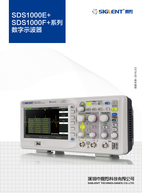
数据手册-2016.03SDS1000E+/SDS1000F+系列数字示波器产品综述SDS1000E+/SDS1000F+系列是一款普及型双通道数字示波器产品,拥有120 MHz 到200 MHz 带宽机型;高达1 Mpts(SDS1000E+)的存储深度,在捕获长信号的同时,保证了精细的波形分辨率;配备7英寸彩色 TFT-LCD (800*480)液晶屏,帮助您更好地洞察信号细节; 1 GSa/s 采样率让您轻松考察瞬时信号;简洁的操作界面保证了示波器的易用性;32种参数自动测量和常用的数学运算功能,大大提升了工作效率,轻松应对复杂信号的测量需求。
特性与优点模拟通道带宽: 120 MHz、200 MHz 实时采样高达1 GSa/s,等效采样50 GSa/s 存储深度达1 Mpts(SDS1000E+机型)5种触发功能:边沿、脉宽、视频、斜率、交替5种数学运算:+、-、*、/、FFT 6位硬件频率计实时计数显示支持12种语言显示及嵌入式在线帮助系统屏幕保护功能(1分钟至5小时)独特的数字滤波和波形记录仪功能便捷的一键式设计,支持一键式打印和存储7英寸TFT-LCD 显示屏,分辨率800*480标准配置接口:USB Host、USB Device(USBTMC)、Pass/Fail、LAN(VXI-11)SDS1000E+/SDS1000F+系列数字示波器型号与主要指标设计特色32种参数自动测量功能,支持5组参数的配置显示一键ZOOM功能SDS1000E+/SDS1000F+系列产品支持电压、时间和延迟测试种类,共计32种参数,用户可根据需求配置5组参数显示,也可全部显示32种参数的测量结果一键式设计的视窗扩展功能可对整体波形的局部做波形扩展显示,极大方便了用户对波形的观察、测量和分析最大存储深度达1 Mpts高达1 Mpts 的存储深度,用户能够使用更高的采样率捕获更长时间的信号,然后快速放大需要关注的区域,保证了精细的波形分辨率,既能纵览全局,也能细节呈现普通存储模式下 长存储模式下(1 Mpts)SDS1000E+/SDS1000F+系列数字示波器设计特色数字记录仪功能嵌入式在线帮助系统丰富的硬件接口数字记录仪功能可实时、无死区的记录波形数据仪器内置7 M 的数据存储空间,支持外部U 盘等存储器扩展支持记录后的波形数据回放功能,适合观测慢速信号的一致性问题SDS1000E+/SDS1000F+支持USB Host、USB Device(USBTMC)、LAN(VXI-11)、Pass/Fail 接口提供多种语言的嵌入式帮助系统,让您在最短的时间内熟悉产品的所有功能按键和设置实用的分析测量功能Pass/Fail测试Pass/Fail 功能可根据用户自定义的垂直和水平容限,将被测信号与创建的模板信号进行比较,适用于长期监测信号或进行生产线测试SDS1000E+/SDS1000F+系列产品提供5种常用的波形运算:+、-、*、/、FFT,支持通道波形和FFT 波形分屏显示,方便用户同时观测SDS1000E+/SDS1000F+系列数字示波器参数规格SDS1000E+/SDS1000F+系列数字示波器SDS1000E+/SDS1000F+系列数字示波器SDS1000E+/SDS1000F+系列数字示波器SDS1000E+/SDS1000F+系列数字示波器探头及选配件SDS1000E+/SDS1000F+系列数字示波器。
GTH1000一氧化碳传感器说明书
GTH10O0一氧化碳传感器使用说明特别提示:安装使用产品前,请仔细阅读产品使用说明书! 版本:第2版日期:2008年3月执行标准:Q/JLD 02-2008« GTHIOOO T用一氧化碳传感器》北京中煤安泰机电设备有限公司GTH1000矿用一氧化碳传感器使用说明书1概述GTH1000矿用一氧化碳传感器是采用进口的电化学敏感元件制成的固定式智能测量仪器,该传感 器适用于煤矿井下各作业场所中测量空气中的一氧化碳浓度。
传感器具有红外线遥控调校功能;具有超 限声、光报警功能。
另外,由于传感器没有调节孔和需要调节的零件, 使得密封性能更好,工作更可靠。
传感器具有多种信号输出制式,可与国内各种监测系统配套使用。
2术语和定义下列术语和定义适用于本标准。
型号G T H 1000 —测量范围:T T —— 敏感元件类型“电化学”代号氧化碳代号产品类型“传感器”代号3基本参数本安参数:U i 21V l i 75mA C i : 0.5nF L i : OmH 。
3.10.1显示稳定性当一氧化碳浓度恒定时,传感器的显示值或输出信号值变化量不超过3.10.2传感器的基本误差应满足下列表 1的要求。
-6 0 〜1000 XW CO3.1 工作环境条件温度:0〜40Ca) b) 相对湿度:W 98% (25C 时)C ) 大气压力: 80kPa 〜116kPad) 风 速:0〜8m/s3.2 e) 工作电压 12— 21VDC煤矿井下具有甲烷气体爆炸性危险的环境中,测量空气中的一氧化碳浓度。
3.3 3.4 贮存温度为(—40〜60)C 。
3.5 输出信号制式:3.6 200〜1000Hz 、 5〜15Hz 、 5〜155Hz 。
传感器以10-6单位表示测量值,采用数字显示( 4位LED ),分辨率:频率: -6 1 X 10 CO 。
3.7 3.9 传感器具有避免因断电而影响化学原理敏感元件工作稳定的措施。
某新能源科技公司产品规格书

某新能源科技公司产品规格书 产品规格书 产品型号: SR-2LT 文件编号: 版本编号: V1.0 发行日期: 2010-3-20
制定 审核 批准 地址:深圳市宝安区西乡鹤洲恒丰工业城C6栋 目 录 1 产品规格 1.1 产品简介 本操纵器专为太阳能路灯系统设计,太阳能庭院灯系统设计,具有两路负载输出,每路可分别实现双时段晨亮功能。同时具有丰富的参数设置,用户能够设置光控点电压、光控推断时间、延时开灯时间、蓄电池类型等,可根据实际环境设置不一致参数,使系统达到最优设置。本产品支持铅酸电池、开口电池、胶体电池、锂铁电池等各类电池的使用,应用范围十分广泛。同时加入先进的自学习算法,能够自动识别夜晚长度,智能的调节二次开灯时间,使定时操纵更加精确。本产品特有测试按键,方便安装调试使用。系统具有短路、过载、与特殊的防反接保护,充满、过放自动关断、恢复等全功能保护措施,全面的充电指示、蓄电池状态、负载及各类故障指示。本操纵器通过电脑芯片对蓄电池电压、光电池电压、放电电流、环境温度等参数进行采样,通过专用操纵模型计算,实现符合蓄电池特性的放电率、温度补偿修正的高准确操纵,并使用了智能高效的PWM模糊充电方式对蓄电池进行充电,使用7段式电压操纵,保证蓄电池工作在最佳状态,大大延长了蓄电池的使用寿命。关于具有自动识别的型号,系统上电时将检测系统电压,假如是12V系统数码管显示“12”;假如是24V系统数码管将显示“24”。
1.2 产品型号识别 SR – 2 L T 24 10 A 额定输出电流 自动识别型号
额定输入电压 产品功能代码,T表示双时段系列 产品型号代码,2L表示双路系列
硕日产品型号 1.3 基本参数 参数 密封电池 开口电池 胶体电池 锂铁电池 空载损耗 <5mA 充电回路压降 不大于0.20V 放电回路压降 不大于0.15V 超压保护 17.0V 提升充电电压 14.6V 14.4V 14.8V 15.0V 直充充电电压 14.4V 14.2V 14.6V 14.8V 浮充电压 13.6V 13.6V 13.8V 14.4V 充电返回电压 13.2V 13.2V 13.2V 13.2V 过放返回电压 12.5V 12.5V 12.4V 12.6V 欠压电压 12.0V 12.0V 11.8V 11.8V 过放电压 11.1V 11.3V 10.8V 10.8V 充电方式 串联PWM 工作温度 -35℃至+65℃ 其中锂铁电池参数仅供参考,可根据用户实际所用电池参数进行修改。
STI1000资料
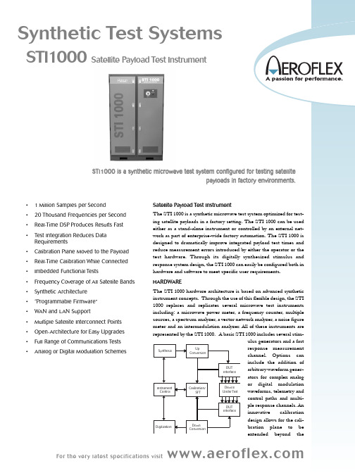
STI1000 Satellite Payload Test Instrument
STI1000 is a synthetic microwave test system configured for testing satellite payloads in factory environments.
• • • • • • • • • • • • • • •
1 Million Samples per Second 20 Thousand Frequencies per Second Real-Time DSP Produces Results Fast Test Integration Reduces Data Requirements Calibration Plane Moved to the Payload Real-Time Calibration While Connected Imbedded Functional Tests Frequency Coverage of All Satellite Bands Synthetic Architecture “Programmable Firmware” WAN and LAN Support Multiple Satellite Interconnect Points Open-Architecture for Easy Upgrades Full Range of Communications Tests Analog or Digital Modulation Schemes
Satellite Payload Test Instrument The STI 1000 is a synthetic microwave test system optimized for testing satellite payloads in a factory setting. The STI 1000 can be used either as a stand-alone instrument or controlled by an external network as part of enterprise-wide factory automation. The STI 1000 is designed to dramatically improve integrated payload test times and reduce measurement errors introduced by either the operator or the test hardware. Through its digitally synthesized stimulus and response system design, the STI 1000 can easily be configured both in hardware and software to meet specific user requirements. HARDWARE The STI 1000 hardware architecture is based on advanced synthetic instrument concepts. Through the use of this flexible design, the STI 1000 replaces and replicates several microwave test instruments including: a microwave power meter, a frequency counter, multiple sources, a spectrum analyzer, a vector network analyzer, a noise figure meter and an intermodulation analyzer. All of these instruments are represented by the STI 1000. A basic STI 1000 includes several stimulus generators and a fast response measurement Up Synthesis Conversion channel. Options can include the addition of DUT arbitrary waveform generInterface ators for complex analog or digital modulation Device Instrument Calibration/ waveforms, telemetry and Under Test Control SFT control paths and multiple response channels. An DUT Interface innovative calibration design allows for the caliDown Digitization bration plane to be Conversion extended beyond the
VOLTECH - Voltech PM1000 Data Sheet

VoltechPM1000+Precision Power Analyzer• Easy to use.• 0.1% basic accuracy.• Special standby power, inrush, and W-hr integration modes.• Comprehensive high-speed interfacing for automated use.• Ideal for the design and test of all electrical products.
Versatile, Accurate, Fully Featured and Easy-to-UseThe No Compromise Power AnalyzerDriven by consumer demand and energy efficiency legislation, tomorrow’s electrical and electronic products must operate with ever-greater efficiency and employ increasingly complex control methods such as a low-power standby operation. The accurate measurement of electrical power has never been more important than it is today.
The Voltech PM1000+ is the first power analyzer to combine bench instrument accuracy with sophisticated energy consumption features and low-power standby measurements at an affordable price. The PM1000+ measures power consumption from milliwatts to megawatts, providing accurate power and harmonic data on products ranging from the tiniest cell phone charger to the latest electric hybrid bus.
Keysight N1000A DCA -X 说明书

N1000A DCA-XWide Bandwidth Oscilloscope Mainframe and ModulesTable of ContentsIntroduction (3)N1000A DCA-X Specifications (4)Module Selection Guide (12)Module Specifications, General Notes (13)54754A (13)86105C (16)86105D (19)86108B (23)86115D (25)86116C (29)N1045A (36)N1045B (39)N1046A (41)N1055A (44)N1060A (49)Modules no longer available but supported by the N1000A DCA-X Mainframe (53)Ordering Information (53)N1000A DCA-X (54)Dual/Quad Electrical Channel Modules (56)TDR/TDT Modules (57)Precision Waveform Analyzer Modules (57)External Clock Recovery Solutions (58)Warranty Options (for All Products) (59)Accessories (60)Connectivity Solutions (60)IntroductionThe N1000A DCA-X performs precision measurements on high speed digital designs from50 MBd to more than 80 GBd on up to 16 channels simultaneously. Applications include: •Optical transceiver design and production test•Electrical ASIC/FPGA/IC design and characterization•Serial bus characterization, measurements and trouble-shooting via TDR/TDT and S-parameter measurements of channels, cables and PCBsKeysight offers complete Digital Communication Analyzer solutions that can be combinedwith or used alongside the DCA-X, including clock recovery, stand-alone Digital Communication Analyzers (DCA-M) and software. For complete information on Keysight’sentire DCA family, please refer to these other helpful documents:•Keysight DCA Wide Bandwidth Oscilloscope Family Brochure•Keysight DCA Family FlexDCA Sampling Oscilloscope Software Technical Overview •Keysight N1000A DCA Wide Bandwidth Oscilloscope Family Configuration Guide, 5992-0038EN•Keysight DCA Family Clock Data Recovery Solutions Data Sheet, 5991-2340EN•Keysight N1090A, N1092A/B/C/D/E and N1094A/B DCA-M Optical and Electrical Sampling Oscilloscope Data Sheet, 5992-1454EN.Optical + Electrical andOptical + Electrical DCA-M FlexDCA Software Electrical Clock RecoveryN1000A DCA-X SpecificationsGeneral NotesNote: All specifications describe warranted performanceover the temperature range +10° C to + 40° C (unlessotherwise noted). The specifications are applicable after thetemperature is stabilized, which occurs after 1 hour ofcontinuous operation in final setup configuration, and whilemodule calibration is valid. Many performance parametersare enhanced through frequent, simple user calibrations.Note: Specifications describe warranted performance. Characteristics provide useful, non-warranted information about the functions and performance of the instrument. Characteristics are printed in green italics.Note: Factory Calibration Cycle. For optimum performance, the instrument should have a complete verification of specifications once every 12 months.Note: Nominal Value indicates the expected, but not warranted, value of the parameter. Computer System and Storage SpecificationsItem DescriptionCPU Intel I5 Quad CoreRAM 8 GBOperating System Windows 10, 64 bitMass Storage 240 GB internal SSD hard diskDisplay SpecificationsItem DescriptionDisplay Area •210.4 mm x 157.8 mm•10.4-inch diagonal color active matrix LCD module incorporating amorphous silicon TFTs.Entire Display Resolution 1024 pixels horizontally x 768 pixels verticallyWaveform Colors Select from over 16 colors. User may change color assignment of all traces (channels, waveform memory, and signal processing functions).Persistence Modes Gray scale, color grade, infinite, variableFind us at Page 4Environmental SpecificationsWarning: The Mains wiring and connectors shall be compatible with the connector used in the premise electrical system. Failure, to ensure adequate earth grounding by not using the correct components may cause product damage, and serious injury.Caution: This product is designed for use in INSTALLATION CATEGORY II and POLLUTION DEGREE 2 environment.Note:Only Keysight approved accessories shall be used.Horizontal (Timebase) Specifications1Dual marker measurement performed at a temperature within ±5° C of horizontal calibration temperature.2Dual marker measurement performed at a temperature within ±1.5° C of horizontal calibration temperature.Input and Output SpecificationsFront-Panel Inputs and Outputs3Dual marker measurement performed at a temperature within ±5° C of horizontal calibration temperature.4 Dual marker measurement performed at a temperature within ±1.5° C of horizontal calibration temperature.5 The time interval resolution is the smallest time you can characterize between two points.Rear-Panel Inputs and OutputsInternal Precision Timebase Specifications (Option PTB) SpecificationsTrigger Specifications SpecificationsTrigger Mode Specifications Internal Trigger ModeClock Trigger/Pattern Lock ModeEdge Trigger Mode6 These specifications refer to the signal input to the front-panel Trigger Input connector. The sampled input signal timing is recreated by using an externally supplied trigger signal that is synchronous with the sampled signal input.7Verified at 10 GHz with a clock and signal slew rate ≥ 15V/ns.8 Verified at 28 GHz with a cloc k and signal slew rate ≥ 20V/ns.9 Verified at 2.5 GHz with a clock and signal slew rate ≥ 2V/nsVertical (Channel) SpecificationsModule Selection GuideModule Specifications, General NotesNOTE:All specifications describe warranted performance over the temperature range +10° C to + 40° C (unless otherwise noted). The specifications are applicable after the temperature is stabilized, which occurs after 1 hour of continuous operation in final setup configuration and while module calibration is valid. Many performance parameters are enhanced through frequent, simple user calibrations.NOTE:Specifications describe warranted performance. Characteristics provide useful, non-warranted information about the functions and performance of the instrument. Characteristics are printed in green italics.NOTE:Factory Calibration Cycle. For optimum performance, the instrument should have a complete verification of specifications once every 12 months.NOTE:Nominal Value indicates the expected, but not warranted, value of the parameter.TDR SystemNormalized information is a characteristic, not a specification. The information is presented here for comparison purposes only. Normalization characteristics are achieved only with the use of the TDR calibration using the firmware routines. Rise time is measured in the Averaged Display mode with best flatness on (default in TDR mode). The rise time of the generator is less than 35 ps, as calculated by:Note:This is a note. Flatness is measured in the Averaged Display mode with best flatness on (default in TDR mode).Caution:This is a caution. Flatness is measured in the Averaged Display mode with best flatness on (default in TDR mode).Warning: This is a warning. Flatness is measured in the Averaged Display mode with best flatness on (default in TDR mode).86105C Module SpecificationsElectrical Channel Specifications86105D Module Specifications86108B Module Specifications86115D Module SpecificationsOptical Channel Specifications (option 025):Optical FWHM at 40 GHz BW. Measured with 1550 nm optical impulse with a pulse of 700 fs FWHM, 5 MHz repetition rate, and 4 mW peak power. System jitter less than 800 fs RMS.Description: 12 ps (characteristic)Electrical Channel Specifications (Option 025)and 30 GHzThis graph shows the electrical channel frequency response (characteristic) at the 80 GHz setting. The blue curve is the unfiltered data, the red curve is a curve fit.Optical Channel Specifications (Option 041)Optical FWHM at 65 GHz BW.Measured with 1550 nm optical impulse with a pulse of 700 fs FWHM, 5 MHz repetition rate, and 10 mW peak power. System jitter less than 800 fs RMS.Description:7.4 ps (characteristic)This graph shows the electrical channel frequency response (characteristic) at the 80 GHz setting. The blue curve is the unfiltered data, the red curve is a curve fit.N1045A Module SpecificationsInput ImpedanceGraph of S11 (Characteristic)N1045B Module SpecificationsInput ImpedanceGraph of S11 (Characteristic)N1046A Module SpecificationsSpecifications10Tuned to be –3 dB (±measurement uncertainty) at stated bandwidth(s), except for 122 GHz which is tuned for highest bandwidth while keeping channel noise ≤ 2.5 mV RMS.Input ImpedanceGraph of S11 (Characteristic)N1055A Module Specifications11 Upgradable from 2 channel to 4 channel after purchase (return to Keysight).12 Connector style is the same on all channels and is selected at time of order.13 Upgradable from 35 GHz to 50 GHz after purchase (return to Keysight).14 Tuned to be –3 dB (±measurement uncertainty) at stated bandwidth(s) using NIST traceable swept-sine test systemTDR System Specifications15 FlexDCA software auto-selects the mainframe or module timebase based on DUT setup. In cases where the mainframetimebase is used, the maximum sample rate will be:86100D Mainframe: 40 kSa/s for standard modules and modules withoption-FS1, (characteristic).N1000A Mainframe: 80 kSa/s for standard modules and 250 kSa/s for modules with option-FS1, (characteristic).16 Incident TDR edge speed is defined as the transition time at the output of the remote head. It is calculatedby de-convolving the receiver transition time from the measured transition time when the remote head is terminated with a short.17 Measured on a negative TDR step, terminated in a short.Step Flatness (Graphs of Combined Oscilloscope and TDR Performance)Performance Characteristics for the N1055A when used with N1010300A Signal Integrity Package for FlexDCA Sampling Oscilloscope SoftwareTest Conditions–Mainframe and module have been turned on for at least one hour and have been calibrated–TDR calibration has been performed using appropriate electronic or mechanical calibration units–Derived from measurements made on 1.85 mm verification devices that were calibrated by Keysight metrology lab –Averages of 512 except as noted in dynamic range49 | Keysight | 86100D-202 Enhanced Impedance and S-Parameter Software for 86100D DCA-X Oscilloscope - Data SheetN1060A Module18 Tuned to be –3 dB (±measurement uncertainty) at stated bandwidth(s), except for 95 GHz which is tuned for highest bandwidth while keeping channel noise ≤ 2 mV RMS.19**************************************************************.20Verifiedwithinputsignal1Vpp@10GHz,*********************************,∼1Vpp to PTB input. 21Ships with ruggedized 1.0 mm (f) to 1.85 mm (f) adaptors.。
仪表规格书模板-电导率分析仪
本体材质 BODY MATERIAL
PES,钛
过程连接 PROCESS CONNECTION
法兰连接
法兰标准及等级 FLANGE STD. & RATING
HG/T 20592-2009
法兰尺寸及密封面 FLANGE SIZE & FACING PN16/DN80/RF
电气接口尺寸 ELEC. CONN. SIZE
型号 MODEL
CLM253-CD0505
变送器形式 TRANSMITTER TYPE
仪表箱内安装
测量范围 MEAS. RANGE
0-10000us/cm
输出信号 OUTPUT SIGNAL
4-20mA +HART
DCS 范围 DCS RANGE
0-10000us/cm
分析周期 RESPONSE TIME
连续
精度 ACCURACY
±1% @ Reading
电源 POWER SUPPLY
220VAC,50Hz,单相
传感器规格 THE SENSOR SPECIFICATION
型号 MODEL
CLS21-C1N2A
量程范围 INSTRUMENT RANGE
0-10000us/cm
插入长度 INSERTION LENGTH
用途 SERVICE
污水电导率
P&ID号 P&ID NO.
操作条件 OPERATING CONDITIONS
工艺介质 PROCESS FLUID
含盐污水
操作压力 OPER.PRES. Mpa(G)
常压
操作温度 OPER.TEMPER. ℃
常温
操作状态下粘度 VISCOSITY AT OPER. MPa.s
skstaae010规格书
skstaae010规格书SKSTAAE010规格书是一份详细描述产品规格和性能的文件。
本文将围绕SKSTAAE010规格书展开,介绍其主要内容和特点。
一、产品简介SKSTAAE010是一款具有高性能和稳定性的产品。
它采用先进的技术和材料制造而成,具有以下特点:1. 高性能:SKSTAAE010产品具有卓越的性能表现。
它能够快速、准确地完成各种复杂任务,满足用户的不同需求。
2. 稳定性:SKSTAAE010产品在各种环境条件下都能保持稳定运行。
无论在高温、低温、高湿度或低湿度环境下,它都能够稳定工作。
3. 耐用性:SKSTAAE010产品采用耐用的材料制造,具有较长的使用寿命。
它能够经受住长时间的使用和各种外部挑战,保持高效运行。
4. 易操作:SKSTAAE010产品具有简单易用的界面和操作方式。
用户可以轻松上手,并快速掌握其功能和特点。
5. 安全性:SKSTAAE010产品具有完善的安全措施,保障用户的信息和数据安全。
它能够有效防止非法访问和恶意攻击,保护用户的隐私。
二、技术规格SKSTAAE010产品的技术规格如下:1. 处理器:采用先进的处理器技术,具有高速运算和强大的计算能力。
2. 存储容量:提供大容量的存储空间,可以存储大量数据和文件。
3. 内存:配置充足的内存,保证系统的运行速度和稳定性。
4. 屏幕:配备高分辨率的屏幕,显示效果清晰、细腻。
5. 连接性:支持多种连接方式,如无线网络、蓝牙等,方便用户进行数据传输和共享。
6. 电池寿命:具有长时间的电池续航能力,能够满足用户长时间使用的需求。
7. 尺寸和重量:体积小巧、重量轻,便于携带和移动。
三、应用领域SKSTAAE010产品具有广泛的应用领域,可以满足各种需求。
主要应用于以下领域:1. 工业控制:SKSTAAE010产品可以应用于工业自动化控制系统,提供高效稳定的控制和监测功能。
2. 通信领域:SKSTAAE010产品可以用于通信设备,提供高速稳定的数据传输和通信功能。
TOC 1000手册
A-1000 TOC 分析系统使用简介AnatelSection 1.A-1000 TOC 分析系统简介1.1 A-1000 TOC 分析系统包括以下部件:C80 显示控制器C80 显示控制器是A-1000 TOC 测试仪的控制/显示部分,一个C80控制器可以分别单独操控多达8个A-1000测试主机,C80显示控制器包括一个4行,16字符宽的显示部件,可以显示诸如:以ppb 为单位的TOC 值,TOC 变化趋势,电阻(或电导),温度以及测试模式。
S10主机是A-1000分析系统的主要部件,在机体上有一个一行,16字符宽的显示部件,可以简单显示机器所测试出的当前的TOC 值。
S10和C80显示控制部件,能与其他的TOC 测试仪协同工作,一个单独的S10主机可以联结多达8个C80显示控制部件,这样就可以在不同的地点同时显示或操控主机。
A-1000 S20测试仪将S10主机和C80显示控制器集成在一个主机上面,使得整个系统更方便携带和随时切换测试的地点。
1.2 A-1000系统特点针对超纯水系统的TOC 测试,A-1000有以下几个显著的特点。
l 快速分析模式快速分析模式可以在最快的速度下得到TOC 的数据,并可以将数据记录下来,这样即使最短暂的TOC 波动也可以被记录下来,当机器的工作模式设置在快速工作模式的时候,仪器可以在最短为2分钟的时间内取得精确的数据。
l 不同地点的TOC 测试有时候,需要同时监测使用点前,后的数据,A-1000分析系统可以支持实时显示两个主机的显示数据,这样,同时比较两个点的数据也成为可行。
l 热水应用A-1000的测试范围为从0-100℃,因此,A-1000系统可以直接测试温度较高的DI 水,这样就可以不需要多余的热交换器来降低水温。
l 独立报警系统A-1000S20P 系统集成了一个单独的热敏打印机,这个打印机也可以联结到任何S10和S20主机1.3 简单原理A-1000 TOC测试系统在测试TOC的过程中不需要化学试剂或气体;系统采用了一种专利测试方法:使用UV灯对水样进行氧化,经过对试样氧化前后电导率的变化来获得相应的TOC值。
半导体传感器ADUM1100ARZ中文规格书
ADuM1400/ADuM1401/ADuM1402Data Sheet Rev. L | Page 14 of 31 ParameterSymbol Min Typ Max Unit Test Conditions ADuM1400WTRWZ /ADuM1401WTRWZ /ADuM1402WTRWZMinimum Pulse Width 3PW 100 ns C L = 15 pF, CMOS signal levels Maximum Data Rate 410 Mbps C L = 15 pF, CMOS signal levels Propagation Delay 5t PHL , t PLH 20 34 45 ns C L = 15 pF, CMOS signal levels Pulse Width Distortion, |t PLH − t PHL |5PWD 3 ns C L = 15 pF, CMOS signal levels Change vs. Temperature5 ps/°C C L = 15 pF, CMOS signal levels Propagation Delay Skew 6t PSK 22 ns C L = 15 pF, CMOS signal levels Channel-to-Channel Matching, Codirectional Channels 7t PSKCD 3 ns C L = 15 pF, CMOS signal levels Channel-to-Channel Matching, Opposing-Directional Channels 7t PSKOD 6 ns C L = 15 pF, CMOS signal levels For All ModelsOutput Disable Propagation Delay(High/Low to High Impedance)t PHZ , t PLH 6 8 ns C L = 15 pF, CMOS signal levels Output Enable Propagation Delay (HighImpedance to High/Low)t PZH , t PZL 6 8 ns C L = 15 pF, CMOS signal levels Output Rise/Fall Time (10% to 90%)t R /t F 3 ns C L = 15 pF, CMOS signal levels Common-Mode Transient Immunity at Logic High Output 8|CM H | 25 35 kV/µs V Ix = V DD1/V DD2, V CM = 1000 V, transient magnitude = 800 V Common-Mode Transient Immunity at Logic Low Output 8|CM L | 25 35 kV/µs V Ix = 0 V, V CM = 1000 V, transient magnitude = 800 V Refresh Ratef r 1.1 Mbps Input Dynamic Supply Current per Channel 9I DDI (D) 0.10 mA/Mbps Output Dynamic Supply Current perChannel 9I DDO (D) 0.03 mA/Mbps 1All voltages are relative to their respective ground. 2 The supply current values for all four channels are combined when running at identical data rates. Output supply current values are specified with no output load present. The supply current associated with an individual channel operating at a given data rate may be calculated as described in the Power Consumption section. See Figure 8 through Figure 10 for information on per-channel supply current as a function of data rate for unloaded and loaded conditions. See Figure 11 through Figure 15 for total V DD1 and V DD2 supply currents as a function of data rate for ADuM1400W /ADuM1401W /ADuM1402W channel configurations. 3 The minimum pulse width is the shortest pulse width at which the specified pulse width distortion is guaranteed. 4 The maximum data rate is the fastest data rate at which the specified pulse width distortion is guaranteed.5 t PHL propagation delay is measured from the 50% level of the falling edge of the V Ix signal to the 50% level of the falling edge of the V Ox signal. t PLH propagation delay is measured from the 50% level of the rising edge of the V Ix signal to the 50% level of the rising edge of the V Ox signal.6 t PSK is the magnitude of the worst-case difference in t PHL or t PLH that is measured between units at the same operating temperature, supply voltages, and output load within the recommended operating conditions.7 Codirectional channel-to-channel matching is the absolute value of the difference in propagation delays between any two channels with inputs on the same side of the isolation barrier. Opposing-directional channel-to-channel matching is the absolute value of the difference in propagation delays between any two channels with inputs on opposing sides of the isolation barrier.8 CM H is the maximum common-mode voltage slew rate that can be sustained while maintaining V O > 0.8 V DD2. CM L is the maximum common-mode voltage slew rate that can be sustained while maintaining V O < 0.8 V. The common-mode voltage slew rates apply to both rising and falling common-mode voltage edges. The transient magnitude is the range over which the common mode is slewed.9 Dynamic supply current is the incremental amount of supply current required for a 1 Mbps increase in signal data rate. See Figure 8 through Figure 10 for information on per-channel supply current for unloaded and loaded conditions. See the Power Consumption section for guidance on calculating the per-channel supply current for a given data rate.ADuM1400/ADuM1401/ADuM1402Data Sheet Rev. L | Page 16 of 31 ParameterSymbol Min Typ Max Unit Test Conditions ADuM1400WTRWZ /ADuM1401WTRWZ /ADuM1402WTRWZMinimum Pulse Width 3PW 100 ns C L = 15 pF, CMOS signal levels Maximum Data Rate 410 Mbps C L = 15 pF, CMOS signal levels Propagation Delay 5t PHL , t PLH 20 30 40 ns C L = 15 pF, CMOS signal levels Pulse Width Distortion, |t PLH − t PHL |5PWD 3 ns C L = 15 pF, CMOS signal levels Change vs. Temperature5 ps/°C C L = 15 pF, CMOS signal levels Propagation Delay Skew 6t PSK 22 ns C L = 15 pF, CMOS signal levels Channel-to-Channel Matching, Codirectional Channels 7t PSKCD 3 ns C L = 15 pF, CMOS signal levels Channel-to-Channel Matching, Opposing-Directional Channels 7t PSKOD 6 ns C L = 15 pF, CMOS signal levels For All ModelsOutput Disable Propagation Delay (High/Lowto High Impedance)t PHZ , t PLH 6 8 ns C L = 15 pF, CMOS signal levels Output Enable Propagation Delay (HighImpedance to High/Low)t PZH , t PZL 6 8 ns C L = 15 pF, CMOS signal levels Output Rise/Fall Time (10% to 90%)t R /t F 3.0 ns C L = 15 pF, CMOS signal levels Common-Mode Transient Immunity at Logic High Output 8|CM H | 25 35 kV/µs V Ix = V DD1/V DD2, V CM = 1000 V, transient magnitude = 800 V Common-Mode Transient Immunity at Logic Low Output 8|CM L | 25 35 kV/µs V Ix = 0 V, V CM = 1000 V, transient magnitude = 800 V Refresh Ratef r 1.2 Mbps Input Dynamic Supply Current per Channel 9I DDI (D) 0.19 mA/Mbps Output Dynamic Supply Current per Channel 9I DDO (D) 0.03 mA/Mbps 1All voltages are relative to their respective ground. 2 The supply current values for all four channels are combined when running at identical data rates. Output supply current values are specified with no output load present. The supply current associated with an individual channel operating at a given data rate may be calculated as described in the Power Consumption section. See Figure 8 through Figure 10 for information on per-channel supply current as a function of data rate for unloaded and loaded conditions. See Figure 11 through Figure 15 for total V DD1 and V DD2 supply currents as a function of data rate for ADuM1400W /ADuM1401W /ADuM1402W channel configurations. 3 The minimum pulse width is the shortest pulse width at which the specified pulse width distortion is guaranteed.4 The maximum data rate is the fastest data rate at which the specified pulse width distortion is guaranteed.5 t PHL propagation delay is measured from the 50% level of the falling edge of the V Ix signal to the 50% level of the falling edge of the V Ox signal. t PLH propagation delay is measured from the 50% level of the rising edge of the V Ix signal to the 50% level of the rising edge of the V Ox signal.6 t PSK is the magnitude of the worst-case difference in t PHL or t PLH that is measured between units at the same operating temperature, supply voltages, and output load within the recommended operating conditions.7 Codirectional channel-to-channel matching is the absolute value of the difference in propagation delays between any two channels with inputs on the same side of the isolation barrier. Opposing-directional channel-to-channel matching is the absolute value of the difference in propagation delays between any two channels with inputs on opposing sides of the isolation barrier.8 CM H is the maximum common-mode voltage slew rate that can be sustained while maintaining V O > 0.8 V DD2. CM L is the maximum common-mode voltage slew rate that can be sustained while maintaining V O < 0.8 V. The common-mode voltage slew rates apply to both rising and falling common-mode voltage edges. The transient magnitude is the range over which the common mode is slewed.9 Dynamic supply current is the incremental amount of supply current required for a 1 Mbps increase in signal data rate. See Figure 8 through Figure 10 for information on per-channel supply current for unloaded and loaded conditions. See the Power Consumption section for guidance on calculating the per-channel supply current for a given data rate.。