音频信号发生器毕业设计论文 翻译 英文--
音频信号处理硕士论文中英文资料外文翻译文献
音频信号处理硕士论文中英文资料外文翻译文献[摘要]本文旨在为音频信号处理硕士论文提供有关外文翻译文献的资料。
以下是一些可能相关的外文文献:1. Title: "Advanced Techniques for Audio Signal Processing"Author: John SmithYear: 2018Abstract: This paper explores advanced techniques in audio signal processing, including noise reduction, speech enhancement, and audio analysis. It provides insights into the latest developments and research in the field.2. Title: "Digital Audio Signal Processing: Principles and Applications"Author: Lisa JohnsonYear: 20153. Title: "Real-Time Audio Signal Processing: Implementations and Applications"Author: Michael AndersonYear: 2012Abstract: This paper focuses on real-time implementations of audio signal processing algorithms and their applications. It discusses techniques for efficient processing in real-time scenarios, such as audio streaming and interactive audio applications.请注意,以上文献仅为示例,并非实际存在的文献。
函数发生器外文文献及翻译
外文文献1原文:DDS devices to produce high-quality waveform: a simple, efficient and flexibleSummaryDirect digital frequency synthesis (DDS) technology for the generation and regulation of high-quality waveforms, widely used in medical, industrial, instrumentation, communications, defense and many other areas. This article will briefly describe the technology, on its strengths and weaknesses, examine some application examples, and also introduced some new products that contribute to the promotionIntroductionA key requirement in many industries is an exact production, easy operation and quick change of different frequencies, different types of waveforms. Whether it is broadband transceiver requires low phase noise and excellent spurious-free dynamic performance of agile frequency source, or for industrial measurement and control system needs a stable frequency excitation, fast, easy and economical to produce adjustable waveform while maintaining phase continuity capabilities are critical to a design standard, which is what the advantages of direct digital frequency synthesis. Frequency synthesis taskThe growing congestion of the spectrum, coupled with lower power consumption, quality of never-ending demand for higher measuring equipment, these factors require the use of the new frequency range, requires a better use of existing frequency range. A result, the search for better control, in most cases, by means of frequency synthesizer for frequency generation. These devices use a given frequency, fC of to generate a target frequency (and phase) fOUT the general relationship can be simply expressed as:fOUT = εx× fCAmong them, the scale factor εx, sometimes known as the normalized frequency.The equation is usually gradual approximation of the real number algorithms. When the scale factor is a rational number, two relatively prime numbers (output frequency and reference frequency) than the harmonic. However, in most cases, εx may belong to a broader set of real numbers, the approximation process is within the acceptable range will be truncatedDirect Digital Frequency SynthesizerThe frequency synthesizer a practical way to achieve is the direct digital frequency synthesis (of DDFS), usually referred to as direct digital synthesis (DDS). This technique using digital data processing to generate a frequency and phase adjustable output, the output anda fixed frequency reference clock source fC. related. DDS architecture, the reference or the system clock frequency divided by a scale factor to produce the desired frequency, the scale factor is controlled by the binary tuning word programmable.In short, direct digital frequency synthesizer to convert a bunch of clock pulses into an analog waveform, usually a sine wave, triangle wave or square wave. Shown in Figure 1, its main parts: the phase accumulator (to produce the output waveform phase angle data), relative to digital converter, (above the phase data is converted to the instantaneous output amplitude data), and digital-to-analog converter (DAC) (the magnitude of data into a sampled analog data points)F igure 1.DDS function of the system block diagram.For the sine wave output, relative to digital converter is usually a sine lookup table (Figure 2). Phase accumulator unit count N a relative to the frequency of fC, according to the following equation:The number of pulses of the fC:M is the resolution of the tuning word (24-48)N corresponds to the smallest increment of phase change of the phase accumulator output wordFigure 2. Typical DDS architecture and signal path (with DACs). Changing N will immediately change the output phase and frequency, so the system has its own continuous phase characteristics, which is one of the key attributes of many applications. No loop settling time, which is different from the analog system, such as phase-locked loops (PLLs). DAC is usually a high-performance circuit, designed specifically for the DDS core (phase accumulator and phase amplitude converter). In most cases, the results of the device (usually single-chip) is generally referred to as the pure DDS or the C-DDS.Actual DDS devices are generally multiple registers, in order to achieve a different frequency and phase modulation scheme. Such as phase register, their storage phase of increase in the output phase of the phase accumulator. In this way, the corresponding delay output sine wave phase in a phase tuning word. This is useful for phase modulation applications for communication systems. The resolution of the adder circuit determines the number of bits of the phase tuning word,therefore, also decided to delay the resolution.Integrated in a single device on the engine of a DDS and a DAC has both advantages and disadvantages, however, whether integrated or not, need a DAC to produce ultra-high purityhigh-quality analog signal. DAC will convert digital sinusoidal output to an analog sine wave may be single-ended or differential. Some of the key requirements for low phase noise, excellent wideband (WB) and narrowband (NB), spurious-free dynamic range (SFDR), and low power consumption. If the external device, the DAC must be fast enough to handle the signal, so the built-in parallel port device is very common.DDS and other solutionsThe frequency analog phase-locked loops (PLLs), clock generator, and the use of FPGA dynamic programming of the output of the DAC. By examining the spectrum of performance and power of these technologies, a simple comparison, Table 1 shows the qualitative results of the comparisonPhase-locked loop is a feedback loop and its components: a phase comparator, a divider and a pressure-controlled oscillator (VCO), phase comparator reference frequency and output frequency (usually the output frequency is N)frequency) were compared. The error voltage generated by the phase comparator is used to adjust the VCO, thus the output frequency. When the loop is established, the output frequency and / or phase with the reference frequency to maintain a precise relationship. PLL has long been considered in a particular frequency range, high fidelity and consistent signal low phase noise and high spurious free dynamic range (SFDR) are ideal for applications.PLL can not be precisely and quickly tuning the frequency output waveform, and the slow response, which limits their applicability for fast frequency hopping and part of the frequency shift keying and phase shift keying applications.Other programs, including integrated DDS engine field programmable gate arrays (FPGAs) - a synthetic sine wave output with the off-the-shelf DAC - though the PLL frequency-hopping problem can be solved, but there own shortcomings. The defects of the major systems work and interface power requirements, high cost, large size, and system developers must also consider the additional software, hardware and memory. For example, using the DDS engine option in the modern FPGA to generate the 10 MHz output signal dynamic range is 60 dB up to 72 kB memory space. In addition, designers need to accept and be familiar with the subtle balance DDS core architecture. .From a practical point of view (see Table 2), thanks to the rapid development of CMOS technology and modern digital design techniques, as well as the improvement of the DAC topology, DDS technology has been able to achieve unprecedented low power consumption in a wide range of applications, spectrum performance and cost levels. Although the pure DDS products in performance and design flexibility to achieve the level of high-end DAC technology and FPGA, but the advantages of DDS in terms of size, power consumption, cost and simplicity, making it the primary choice for many applications.Table 2 Benchmark Analysis Summary - frequency generation technique (<50MHz)Phase -locked loop DAC + FPGA DDS Spectral performance High High Middle System power requirements High High Middle Digital frequency tuning No Yes Yes Tuning response time High Low Low Solution size Middle High Low Waveform flexibility Low Middle High Cost Middle High Low Design reuse Middle Low High Implementation complexity Middle High Low Also be noted that the DDS device for digital methods to produce the output waveform, it can simplify some of the architecture of the solution, or the waveform of digital programming to create the conditions. Usually with a sine wave to explain the functions and working principle of the DDS, but using modern DDS ICs can easily generate a triangle wave or square wave (clock) output, thereby eliminating the former case the lookup table, and the latter case the DAC the need to integrate a simple and accurate enough.Performance and limitations of the DDSImage and envelope: Sin (x) xx roll-offThe actual output of the DAC is not a continuous sine wave, but a series of pulses with a sinusoidal time envelope. The corresponding spectrum is a series of image and signal aliasing. Image along the sin (x) / x envelope distribution (see Figure 3 | margin | graph). The need for the filter to suppress frequencies outside the target band, but can not inhibit the high-level in the passband aliasing (for example, caused due to DAC non-linear)The Nyquist criterion requires that each cycle requires at least two sampling points in order to rebuild the desired output waveform. The Mirroring response arising from sampling the output frequency K, CLOCK × OUT In this example, which CLOCK = 25 25 MHz and fOUT = 5 MHz, the first and second mirror frequency appear in (see Figure 3) fCLOCK × fOUT, o 20 MHz and 30 MHz. The third and fourth mirror frequency at 45 MHz and 55 MHz. Note, sin (x) / x value of zero at multiples of the sampling frequency. When fOUT greater than the Nyquist bandwidth (1/2 f CLOCK), the first mirror frequency will appear in the Nyquist bandwidth, the occurrence of aliasing (such as 15 MHz signal aliasing down to 10 MHz). Can not use the traditional quistanti-aliasing filter to filter out aliasing mirror frequency from the outputSin, in Figure 3.DDS, (x) / x roll-off.In a typical DDS application, the use of a low-pass filter to suppress the mirror frequency response of the output spectrum. To make the low-pass filter cutoff frequency to remain at reasonable levels, and keep it simple filter design, a feasible approach is the use of an economic low-pass output filter bandwidth limited to about 40% of the frequency of clock.Any given mirror frequency relative to the amplitude of the fundamental formula of sin (x) / x calculation. Because the function of the frequency roll-off, the basic output of the amplitude and the output frequency is inversely proportional to decrease; in the DDS system, reduce the amount of DC-Nyquist bandwidth range of -3.92 dB.Significant reduction in frequency in the first mirror - the fundamental 3 dB range. In order to simplify the DDS application filtering, frequency plan must be formulated and analyzed to mirror the frequency and magnitude of the sin (x) / x response in the OUT and CLOCK target frequency spectrum requirements. Other unwanted frequencies in the output spectrum (such as integral and differential linearity error of the DAC, the surge of energy associated with the DAC and clock feed through noise) does not follow the sin (x) / x roll-off response. These unwanted frequencies will be harmonic and spurious energy in the output spectrum in many places - but its magnitude is generally far below the mirror frequency response. DDS devices to the general background noise, substrate noise, thermal noise effects, ground coupling and other signal source coupling factor cumulative portfolio decisions. DDS devices, the noise floor performance of stray and jitter by the circuit board layout, power quality, and - most importantly - Enter the profound impact of the quality of the reference clock.ShakeThe edge of the perfect clock source will be the precise time interval, the interval will never change. Of course, this is not possible; even the best oscillator is also the ideal components constitute, with noise and other defects. Quality and low phase noise crystal oscillator jitter picosecond, and is built up from one million the number of clock edge. The factors leading to jitter external interference, thermal noise, the oscillator circuit instability and power, ground and output connections bring, all these factors will interfere with the timing characteristics of the oscillator. In addition, the oscillator by the external magnetic field or electric field and the nearby transmitter RF interference. Oscillator circuit, a simple amplifier, inverter or buffer to signal additional jitter. Therefore, the choice of a low-jitter, and the edge of steep stable reference clock oscillator is critical. Higher frequency reference clock allows a larger sample, and divide to some extent, reduce the jitter, because the signal to divide a long time to produce the same amount of jitter, which can reduce the jitter on the signal percentage.Noise - including the phase noiseThe sampling system noise depends on many factors, the most important factor is the reference clock jitter, this jitter performance of phase noise on fundamental signal. In the DDS system, the register output of the truncated phase may bring the system error code. The binary word does not lead to the truncation error. But for non-binary word, phase noise truncation error in the spectrum spurious. Spurious frequency / amplitude depends on the code word. Quantification and linearity error of the DAC will be brought to the system harmonic noise. Time-domain error (such as owed to the red / overshoot and code errors) will increase the output signal distortion.ApplicationDDS applications can be divided into two categories:Require agile frequency source for data coding and modulation applications, communications and radar systemsRequire measurement of the universal frequency synthesizer features and programmable tuning, scanning, and motivational skills, industrial and optical applicationsBoth cases, the trend toward higher spectral purity (low phase noise and higher spurious free dynamic range), also low power and small size requirements to accommodate the remote ordemand for battery-powered devices.Modulation / data encoding, and synchronization of the DDSDDS products first appeared on the radar and military applications and the development of some of its characteristics (performance improvements, cost and size, etc.) DDS technology is becoming more prevalent in the modulation and data encoding applications. This section will discuss the two data encoding scheme in the DDS system.Binary frequency shift keying(BFSK, or referred to as FSK) one of the most simple form of data encoding.The launch of the data is a continuous carrier frequency in two discrete frequency (binary one, ie, pass number, a binary 0, namely, the transformation between the space). Figure 4 shows the relationship between the data and transmit signals.Figure 4 binary FSK modulation.Binary 1 and 0 for two different frequencies f0 and f1, respectively. This encoding scheme can be easily DDS device. On behalf of the output frequency of the DDS frequency tuning word change to f0 and f1, will launch the 1 and 0. To transform the output frequency shall dedicated pin FSELECT, containing the appropriate tuning word registers (see Figure 5)Figure 5. AD9834 or AD9838 DDS tuning word selector realization of the FSKencoding.Phase shift keying (PSK) is a simple form of data encoding. In PSK, the carrier frequencyremains the same, by changing the phase of the transmitted signal to transmit information. Can take advantage of a variety of programs to achieve PSK,. The easiest way is often referred to as binary PSK (BPSK), using only two signal phase: 0 ° (logic 1) and 180 ° (logic 0). Members state depends on the status of the former one. If the wave phase remains unchanged, the signal state will remain the same (low or high). Wave phase change 180 °, ie, phase inversion, the signal state will change (low into high or high to low). PSK coding in DDS products can be easily achieved, because most devices have a separate input register (phase register), and phase values can be loaded. This value is added directly to the carrier phase, without changing its frequency. Change the contents of the register will be modulated carrier phase, resulting in a PSK output. For applications that require high-speed modulation, built-in phase register of the AD9834 andAD9838 allow PSELECT pin signal transformation, according to need modulated carrier in the preloaded phase registers.The more complex the PSK four or eight-wave phase. Thus, whenever the phase change of binary data transfer rate will be higher than the BPSK modulation. In the four-phase modulation (Quadrature PSK), in the phase angle of 0 ° to +90 °, -90 ° and +180 °; each phase to transform the two signals may represent a factor AD9830, AD9831, AD9832, and the AD9835 provides four phase registers, can be continuously updated register of different phase shift, the complex phase modulation scheme.The use of synchronous mode of multiple DDS devices to achieve the I / Q Multiple DDS components to achieve the many applications of the I / Q sine wave or square wave signal of known phase relationship between two or more synchronous mode. A common example is the same phase and quadrature modulation (I / Q) in this technique, the phase angle of 0 ° and 90 ° from the carrier frequency signal information. To run two separate DDS components, you can use the same source clock to output can directly control and manipulate the signal of the phase relationship. In Figure 6, with a reference clock on the AD9838 device programming; the RESET pin is used to update the two devices. In this way, you can achieve a simple I / Q modulation RESET after power and initialized before any data to the DDS transmission. DDS output results can be placed in a known phase, making it a common reference point of view, in order to synchronize multiple DDS devices. When new data is sent to multiple DDS devices, the DDS can remain relevant phase relationship, or by the phase offset register can predict the relative phase shift between the adjustments of multiple DDS. The AD983x series of DDS products have a 12 phase resolution, the effective resolution of 0.1 °.Figure 6. Synchronize the two DDS components.Author: Brendan Cronin[*************************]ADI core products andtechnologies (CPT), a product marketing engineer. Brendan joined the ADI, in 1998 and worked for six years in the industrial and automotive products sector, as mixed-signal design engineers. Brendan is currently the main linear and related technologies.外文文献1翻译:DDS器件产生高质量波形:简单、高效而灵活摘要直接数字频率合成(DDS)技术用于产生和调节高质量波形,广泛用于医学、工业、仪器仪表、通信、国防等众多领域。
信号发生器(毕业设计正文)
4.4软件仿真17
第五章结论21
参考文献22
附录25
第1章绪论
1.1
随着电子测量及其他部门对各类信号发生器的广泛需求及电子技术的迅速发展,促使信号发生器种类增多,性能提高。尤其随着70年代微处理器的出现,更促使信号发生器向着自动化、智能化方向发展。现在,许多信号发生器带有微处理器,因而具备了自校、自检、自动故障诊断和自动波形形成和修正等功能,可以和控制计算机及其他测量仪器一起方便的构成自动测试系统。当前信号发生器总的趋势是向着宽频率覆盖、低功耗、高频率精度、多功能、自动化和智能化方向发展。
XTAL1:反向振荡放大器的输入及内部时钟工作电路的输入。
XTAL2:来自反向振荡器的输出。
3.芯片擦除:
整个PEROM阵列和三个锁定位的电擦除可通过正确的控制信号组合,并保持ALE管脚处于低电平10ms来完成。在芯片擦操作中,代码阵列全被写“1”且在任何非空存储字节被重复编程以前,该操作必须被执行。
1.3
1.能产生正弦波、三角波、方波等常见信号。
2.电路板性价比高,可靠性强,操作简单。
第
2.
信号发生器的实现方法通常有以下几种:
方案1:用分立元件组成的函数发生器,但通常是但函数发生器且频率不高,工作不稳定,不易调试。
方案2:可以由晶体管、运放IC等通用器件制作,更多的则是用专门的函数信号发生器IC产生。如L8038、BA205、XR2207等,他们的功能较少,精度不高,频率上限低,无法产生高频率信号,调节方式不够灵活,频率和占空比不能独立调节,二者相互影响。
3.键盘:用按键来控制数值的输入和输出波形的种类。
4.显示部分:示波器显示波形,采用LCD显示波形.1
信号发生系统主要由CPU、D/A转换电路、放大及I/V转换电路、按键和显示电路、电源等电路组成。
音频和语音信号分析中英文对照外文翻译文献
中英文对照外文翻译原文:Time Varying autoregressive modeling of Audio and speech signalsConventional linear predictive techniques for modeling of speech and audio signals are based on an assumption that a signal is stationary within each analysis frame. However,natural signals are often continuously timevarying, i.e., nonstationary.Therefore this assumption might not be well justified.In this paper, we study a timevarying autoregressive(TVAR) modeling technique in which this restriction is relaxed.A frequency-warped formulation of the Subba RaoLiporace TVAR algorithm is introduced in the article. Theapplicability of the presented methodology to various speechand audio signal processing tasks is illustrated and discussed.It is also shown that the TVAR scheme yields an efficientparametrization for timevarying sounds. 1 IntroductionLinear prediction, LP, is a standard technique in speech and audio coding [1] and in several other applications for analysis and synthesis of audio and speech signals. Conventional LP techn- iques utilize framebased autoregressive spectral modeling,e.g., autocorrelation or autocovariance method of LP.In conventional LP, it is assumed that a signal x(t) can beexpressed as a linear com bination of the previous samples by1()()(),1,...,pk k x t a x t k e t t p T ==-+=+∑ (1)Here, ak are a set of fixed set of p coefficients which can be estimated from a signal frame of T samples, and e(t) is a prediction error, or a residual, signal.In warped LP [2], this is modified by replacing x(t−k) in (1) by dk[x(t)] that is produced by filtering x(t) with a chain of k first-order allpass filters. The transfer function of the allpass filter is of the form 11()()/(1)D z z z λλ--=-+-. Here, λ is called a warping parameter. With =0λ, the system reduces to the conventional linear prediction, and other choices yield to the modified, warped, frequency representation of the system. In speech and audio applications it is beneficial to choose λsuch that the new frequency representation approximates that of human hearing [3, 4]. The signal model for warped linear prediction, WLP, is given by1()[()](),1,...,p k k k x t a d x t e t t p T==+=+∑ (2)This is clearly a generalization of the conventional LP (which is obtained if λ= 0). In practice, the only difference is that all unit delays z−1 in the computation of the correlation values and in the implementation of inverse and synthesis filters are replaced by firstorder allpass elements D(z)[5, 4]. The estimation of the coefficients in both conventional and warped linear prediction relies on an inherent assumption that the signal is stationary within the analysis frame. In many cases this assumption is reasonable. Nevertheless, speech and audio signals are often nonstationary. Onsets and offsets of musical sounds, brief transients, transitions, and chirps are typical examples of nonstationarities which may occur within a timescale that is significantly shorter than the typical length of the analysis frame in the LP analysis. In fact, those are all typical instances in which the conventional LP techniques, e.g., LPbased coders, usually fail. A partial solution this is to perform analysis using overlapping frames and interpolating coefficients, usually linearly, between adjacent signal frames. However, this approach is more or less arbitrary and is not related to the actual fluctuations in the signal.Timevarying autoregressive, TV AR, models were first introduced in [6] and has thereafter been partially reformulated and applied to speech [7, 8]. In this article, a frequencywarped version of the conventional algorithm for directform timevarying filters is presented.2 Warped TV AR ModelsIn the timevarying case the prediction coefficients ,k=1,...,k a p in (1) are functions of time and the model of a signal x(t) is of the form1()[()](),1,...,pk k k x t a d x t e t t p T ==+=+∑ (3)In (3) there are more parameters than data. Thus there are infinitely many exact solutions that fulfill ,most of which are totally meaningless. The determination of timevarying prediction coefficients is an illposed problem and it is characteristic for the class of inverse problems. Without any further prior information or feasible assumptions the problem is almost impossible to solve. It is possible to use, e.g., adaptive filtering [9] or smoothness priors TV AR techniques[10] to estimate the timevarying coefficients.However, these do not immediately lead to the efficient parametrization of the process. The technique presented in this article is based on an assumption that the coefficient evolutions ()k a t can be expressed as linear combinations of predefined basis functions ()t φ, i.e.,0()=()Mk k a t c t φ=∑ (4)where k c are basis coefficients.Substitution of (4) to (3) yields to=01()=()[()](),1,...,pM k k k x t c t d x t e t t p T φ=+=+∑∑ (5)The basis coefficients are obtained by minimizing the residual in least squares sense, i.e., by solving min22min c c X H - (6)Here the parameter vector is of the form1010(,...,,...,,...,)T M p pM c c c c c = (7)1(,...,)T p T X x x +=, and the regressor matrix1010(,...,,...,,...,)M p pM H H H H H = (8)where((1)[(1)],...,()[()])T k k k H p d x t T d x T φφ=++ (9)In Eqs (7)-(9)中()T⋅. denotes transpose. The solution of (6) is formally obtained from1()T T C H H H X -=, although the utilization of an orthogonalization algorithm might beappropriate. The timevarying prediction coefficients are assembled via (4).It is observed that the computational complexity of the algorithm depends on the number of the basis functions and the order of the model. In principle, the computational burden is M times higher than in the usual time-invariant case. However, the modeling capabilities of the time-varying scheme could be better than the time-invariant one. Thus, the extra computational burden is may be acceptable. 3 ExamplesThe following highly simplified example illustrates the applicability of TV AR techniques to LPC based audio coding. In this case, there are only two basis functions and the system is unwar- ped, i.e., =0λ. The signal in Fig. 1 (top) is a segment of an audio signal in which the beginning is an attenuating sound of Vibraphone and in the middle of the frame is an onset of a sound of an acoustic guitar.Figure 1: Top: An excerpt from a musical signal.Bottom:Basis functions of the TVAR modelThe basisfunctions t φ are shown in Fig. 1.The firstbasis function is constant and the secon- d one is a sigmoidal function. If only the first basis function was used the techniquewould be ana-logous to the conventional framebasedLPC. In this example, the center and the steep- ness of thesecond basis function have been chosen using an iterative algorithm that tries to maximize Segme- ntal Prediction Gain ,given by2102110log 2kk S x db k e SPG σσ=∑ (10)Here, the original signal and the residual are divided into S segments and the variance ofeach signal and residual segments are denoted by 2k x σand 2k e σ, respectively. The final result of the TVAR analysis, that is, the coefficient evolution sequences over the signal frame, using the basis function of Fig. 1, are shown in Fig. 2. In this example, the filters corr esponding TVAR models are stable at each time instant. The potential instabilities of TVARmodels[7] can be handled, for example, withmetho- ds discussedin [11, 12].Figure 2: Time-varying coefficient evolutions ak(t).The prediction error signal, residual, of a 10th order TVAR model is shown in Fig. 3 (top). The residual of a conventional 20th order LPC is also shown in Fig 3 (bottom).In the latter case the LPC has been estimated by using Hamming window and autoc- orrelation method of LP. Since there are only two basis functions in the TVAR model, the number of parameters in both cases is the same. However, in TVAR scheme it is necessary to transmit two additional param- eter which describe the center and steepn- ess of the basis function. The prediction gain, PGdB, over the whole signal excerpt in the two cases is approximately the same. SPGdB is higher in the case of the TVAR model, i.e., 43 dB for the TVAR model and 38 dB for the LPC model. The difference between the two techniques is even higher in the Vibr aphone part of the signal, i.e., the PGdB in the TVAR exceeds that of the LPC model by more than 6 dB. This means that the LPC model for the beginning of the excerpt is inaccurate. It is probable, that in a coding applica- tion this would produ- ce an artifact which is sometimes called the preecho effect.Figure 3: Residual signal in the case of a 10th order TVARmodel (top) and 20th order conventional LPC model (bottom) The top panel of Fig. 4 shows a waveform of a male speech utte- rance /ma/ at the sampling rate of 10 kHz. The middle figure shows a set of seven prolate sphe roidal basis functions and a constant function. The bottom figure shows coefficient evolutions of a 12thorder warped TVAR model of the signal. At this sampling rate, = 0.46 yields a frequency representation which very close to the frequency resolution of human hearing [3]. Computing the frequency response of the timevarying filter at each time instant one may produce a representation which is here called an allpole spectrogram.Figure 4: (Top) Original male speech utterance /ma/ (Middle)A set of prolate spheroidal basis functions (Bottom) CoefficientevolutionsFor this coefficient evolution this is shown in Fig. 5d. Fig. 5b shows the allpole spectrogramcorrespond- ing to the unwa- rped case, i.e., =0.Figure 5: Allpole spectrograms corresponding to the estimated parametric models.Panels a and c in Fig. 5 show allpole spectro grams estimated using conventional and war ped LP, respectively, such that the length of the Hanning window was 40 ms and the model was estimated at intervals of 1 ms. The total num ber of parameters for the panels a and c is 200 × 12 = 2400 while in panels b and d it is only 8 × 12 = 96. As expected, the use of warping in panels c and d enhances frequency resolution at low frequencies, e.g., the second formant and the nasal formants at low frequencies are clearly visible in the two bottom panels. According to psychoac- oustic theories and listening test results [4], this is advantageous in many speech and audio appl- ications.4DiscussionThe representation of timevarying coefficients as a linear combination of predefined basis functions provides interesting tools for signal analysis and synthesis. Typically basis functions are elementary mathematical functions, e.g., sinusoids, Gaussian pulses, sigmoids, or prolate spheroidal functions. In all these cases the time scale can be adjusted by changing a single para meter. For example, in synthesis of isolated sou- nds, it is easy to change the duration of each basis function to synthesize signals with different duration but same spectral content. However, this requires that there is also a scalable representation for excitation signal. In a practical experi- ment, the current authors used a simplified multipulse excitation for the warped TVAR model ofspeech utterance/ma/, shown in Fig. 5. By changing the duration of basis functions and the pul- se locations to match the new time scale it was possible to synthesize natural sounding speech sounds where the duration and the pitch of the speech utterance was inchanged but formant traje- ctories were preserved. The use of a warped TVAR model also enhanced the naturalness of synt- hesized sound in this example. The economical parametrization of a time-varying spectrum mak- es TVAR techniques attractive for identification and recognition of speech and sound signals. In these applications the ease of applying time-scaling techniques to basis functions also makes it possible to simplify the recognition of , e.g., isolated speech utterances independently of their va- rying durations. Nevertheless, the TVAR techniques studied in this article do have severe draw- backs. Stability of the model cannot be guaranteed in fact, it is often the case that the estimated model is temporarily instable. There are techniques for stabili- zation of TVAR models [11, 12] but they are computationally expensive and may give too smooth spectral models. The comput- ational burden and memory requirements are high, in Eg. (6), if the signal is long, the order of the model is high, and the numb- er of basis functions is high. For example, a 40th order model with 20 basis functions for a 20 ms wideband speech or audio sample at the sampling rate of 44.1 kHz already yields a regression matrix H having more than 700000 elements. In addition, the time varying directform filter coefficients are not a natural representation for the time varying processes occurring in typical natural sound sources. For example, a monotonic evolution of directform filter coefficients do not convey a smooth transition of a resonance in the frequency domain. Grenier has introduced a related technique based on the TVAR formulation of the lattice method [8]. To put it briefly, recent experience of the current authors is that this technique, and its warped counterpart, has all favorable characteristics of the presented TVAR methods but it also gives solutions to the afore- mentioned problems.译文:基于时变自回归模型的音频和语音信号分析对音频和语音信号的分析,所使用的传统线性预测模型是基于所分析的音频和语音信号是平稳的这一假设。
pcm编码英文作文600字
pcm编码英文作文600字The Essence of PCM Encoding.In the realm of digital audio, Pulse Code Modulation (PCM) stands as a fundamental encoding method that has revolutionized sound reproduction. PCM converts analog audio signals, which are continuous and varying, into digital signals composed of discrete samples. This transformation is not only crucial for digital storage and transmission but also enables unprecedented precision and quality in sound reproduction.At its core, PCM encoding relies on three key principles: sampling, quantization, and coding. Sampling involves capturing analog audio signals at regular intervals, converting them into discrete samples. The rate at which these samples are taken, known as the sampling rate, is crucial for maintaining audio quality. Higher sampling rates, such as 44.1 kHz or 96 kHz, provide a more faithful representation of the original analog signal.Quantization is the next step, where each sample is approximated to the nearest value within a finite set of levels. This process introduces some degree ofapproximation error, but it is carefully managed to ensure that the resulting digital signal retains the essential characteristics of the original analog signal. The numberof quantization levels, determined by the bit depth or resolution, affects the dynamic range and audio quality. Common bit depths for PCM audio include 16 bits and 24 bits.Coding, the final stage of PCM encoding, involves representing the quantized samples as binary data. This binary data can then be stored or transmitted, enabling the reproduction of audio signals in digital devices. PCM encoding is lossless, meaning that the original analogsignal can be perfectly reconstructed from the digital data, provided that the sampling rate and bit depth aresufficient.The widespread adoption of PCM encoding has been instrumental in the development of high-quality audiosystems. It has enabled compact digital storage formatslike Compact Discs (CDs) and high-resolution audio formats like FLAC and ALAC, which offer exceptional sound quality. Additionally, PCM encoding has played a pivotal role in digital audio transmission, enabling lossless streaming services like TIDAL and high-resolution audio streaming on platforms like Qobuz.In conclusion, Pulse Code Modulation encoding has revolutionized the way we listen to music and enjoy audio content. Its ability to faithfully represent analog audio signals in a digital format has opened up new possibilities for audio storage, transmission, and reproduction. As technology continues to evolve, PCM encoding remains a fundamental building block for high-quality audio experiences.。
基于DDS的信号发生器的设计的相关英文文献
基于DDS的信号发生器的设计的相关英文文献及翻译Direct Digital Synthesizer (DDS) is a type of frequency synthesizer used for creating arbitrary waveforms from a single, fixed-frequency reference clock. Applications of DDS include: signal generation, local oscillators in communication systems, function generators, mixers, modulators,sound synthesizers and as part of a digital phase-locked loop.直接数字频率合成(DDS)是一种用于产生任意波形从一个单一的,固定频率的参考时钟的频率合成器。
DDS的应用领域包括:信号的产生,在通信系统中,函数发生器,混频器,调制器,声音合成器和本地振荡器作为一个锁相环数字环路的一部分。
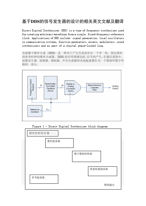
Figure 1 - Direct Digital Synthesizer block diagram图1 - 直接数字频率合成器框图A basic Direct Digital Synthesizer consists of a frequency reference (often a crystal or SAW oscillator), a numerically controlled oscillator (NCO) and a digital-to-analog converter (DAC) as shown in Figure 1.The reference provides a stable time base for the system and determines the frequency accuracy of the DDS. It provides the clock to the NCO which produces at its output a discrete-time, quantized version of the desired output waveform (often a sinusoid) whose period is controlled by the digital word contained in the Frequency Control Register. The sampled, digital waveform is converted to an analog waveform by the DAC. The output reconstruction filter rejects the spectral replicas produced by the zero-order hold inherent in the analog conversion process.A DDS has many advantages over its analog counterpart, the phase-locked loop (PLL), including much better frequency agility, improved phase noise, and precise control of the output phase across frequency switching transitions. Disadvantages include spurious due mainly to truncation effects in the NCO, crossing spurious resulting from high order (>1) Nyquist (尼奎斯特定理) images, and a higher noise floor at large frequency offsets due mainly to the Digital-to-analog converter.Because a DDS is a sampled system, in addition to the desired waveform at output frequency Fout, Nyquist images are also generated (the primaryimage is at Fclk -Fout, where Fclkis the reference clock frequency). In orderto reject these undesired images, a DDS is generally used in conjunction with an analog reconstruction lowpass filter as shown in Figure 1.The output frequency of a DDS is determined by the value stored in the frequency control register (FCR) (see Fig.1), which in turn controls the NCO's phase accumulator step size. Because the NCO operates in the discrete-time domain, it changes frequency instantaneously at the clock edge coincident with a change in the value stored in the FCR. The DDS output frequency settling time is determined mainly by the phase response of the reconstruction filter. An ideal reconstruction filter with a linear phase response (meaning the output is simply a delayed version of the input signal) would allow instantaneous frequency response at its output because a linear system can not create frequencies not present at its input.The superior close-in phase noise performance of a DDS stems from the fact that it is a feed-forward system. In a traditional phase locked loop (PLL), the frequency divider in the feedback path acts to multiply the phase noise of the reference oscillator and, within the PLL loop bandwidth, impresses this excess noise onto the VCO output. A DDS on the other hand, reduces the reference clock phase noise by the ratio f clk/f out,because its output is derived by fractional division of the clock. Reference clock jitter translates directly to the output, but this jitter is a smaller percentage of the output period (by the ratio above). Since the maximum output frequency is limited to f clk/2, the output phase noise at close-in offsets is always at least 6dB below the reference clock phase-noise.At offsets far removed from the carrier, the phase-noise floor of a DDS is determined by the power sum of the DAC quantization noise floor and the reference clock phase noise floor.一个DDS以上的锁相回路(PLL),其模拟对应,许多优势,包括更好的频率灵活性,提高了相位噪声,整个频率转换开关的输出相位的精确控制。
音频信号发生器毕业设计论文
基于LabVIEW的音频信号发生器的虚拟仪器设计摘要:随着计算机与微电子技术的发展,出现了虚拟仪器。
它以软件为核心,把计算机技术和仪器技术完美结合起来,充分应运飞速发展的计算机技术来实现和增强传统仪器的功能。
虚拟仪器开创了仪器使用者可以成为设计者的新时代,代表了仪器发展的方向,它已成为21世纪测试技术和仪器技术发展的主要方向。
本设计正是顺应仪器发展的趋势,利用图形化编程软件LabVIEW来实现虚拟音频信号发生器,真正做到“软件即硬件”。
在硬件上还提出以PC声卡代替昂贵商用数据采集卡,大大降低了生产成本,实现了基于LabVIEW的常用周期信号的单通道和双通道模拟输出,使设计具有广阔的开发价值和应用前景。
论文在简要介绍了虚拟仪器概念、研究现状、发展趋势以及编程软件LabVIEW特点的基础上,概述了音频信号发生器的基本原理,分析了声卡的功能及相关设置,并对构成系统的各模块做了详细叙述。
关键词:虚拟仪器;音频信号发生器;LabVIEW;声卡Virtual Audio Signal Generator Based on LabVIEWAbstract: With the development of computer and microelectronics technology, virtual instruments appear. Virtual instruments achieve the perfect combination of computer science technology and instrument technology through taking the software as the core technology. Virtual instruments realize and enhance the functions of traditional instruments by developing computer technology .Virtual instruments initiate the new era that the instrument users can be the instrument designers. Virtual instruments represent the direction of instruments and it has become the main direction of technological development in the 21st century testing technology and instruments. This design used graphical programming software LabVIEW to design virtual audio signal generator, exactly adjusting the trend of the instrument development, and truly achieve "software that is hardware". In order to reduce production costs and implement single - channel and dual - channel output of common analog periodic signals based on LabVIEW, the design also bring forward to replace the expensive commercial data acquisition card with PC sound card. It has broad application and development prospect. Based on brief introduction of virtual instruments concept, present conditions ,developing trends and characteristics of programming software LabVIEW ,the basic principles of audio signal generator are outlined , the function and relative configurations of sound card are analyzed, and details of each system composing module is presented.Key words: virtual instrument; audio signal generator; LabVIEW; sound card目录1 绪论 (1)1.1 课题背景 (1)1.2 虚拟仪器概述以及国内外研究现状 (1)1.2.1 虚拟仪器概述 (1)1.2.2 虚拟仪器国内外研究现状 (3)1.3 课题的意义 (4)1.4 课题内容 (5)2 系统基本功能描述及软硬件概述 (6)2.1 系统基本功能描述 (6)2.2 软件LabVIEW概述 (6)2.2.1 LabVIEW的结构 (7)2.2.2 LabVIEW模板分析 (8)2.2.2.1 工具模板(Tools Palette) (8)2.2.2.2 控制模板(Controls Palette) (9)2.2.2.3 功能模板(Functions Palette) (10)2.3 硬件声卡概述 (11)2.3.1 声卡工作原理 (11)2.3.2 声卡的工作流程 (12)2.3.3 声卡主要技术指标 (12)3 系统整体方案和各组成部分方案设计 (13)3.1 系统整体方案设计 (13)3.2 波形发生部分方案设计 (13)3.2.1 仿真信号发生器Simulate Signal. vi (15)3.2.2 多谐信号附加噪声的波形发生器Tones and Noise Waveform .vi (17)3.2.3 公式节点产生仿真信号 (19)3.3 声音输出部分方案设计 (21)3.4 图形显示部分方案设计 (22)3.4.1 Waveform Chart (22)3.4.2 Waveform Graph (24)3.4.3 XY Graph (25)4 音频信号发生器系统的设计与结果显示 (26)4.1 音频信号发生器前面板的设计 (26)4.2 音频信号发生器流程图设计 (28)4.3 音频信号发生器运行结果显示 (31)4.3.1 单声道音频信号发生器运行结果显示 (31)4.3.2 双通道音频信号发生器运行结果显示 (32)5 音频信号发生器系统的调试和结果分析 (34)6结论............................................................................................... 错误!未定义书签。
基于DDS技术的信号发生器的设计与实现_毕业设计(论文)

毕业设计设计题目:基于DDS技术的信号发生器的设计与实现基于DDS技术的信号发生器的设计与实现摘要DDS是直接数字式频率合成器(Direct Digital Synthesizer)的英文缩写。
与传统的频率合成器相比,DDS具有低成本、低功耗、高分辨率和快速转换时间等优点,广泛使用在电信与电子仪器领域,是实现设备全数字化的一个关键技术。
本设计采用单片机为核心处理器,利用键盘输入信号的参数,控制DDS的AD9850模块产生信号,信号的参数在LCD1602上显示,完成正弦信号和方波信号的输出,用示波器输出验证。
DDS是一种全数字化的频率合成器,由相位累加器、波形ROM、D/A转换器和低通滤波器构成。
时钟频率给定后,输出信号的频率取决于频率控制字,频率分辨率取决于累加器位数,相位分辨率取决于ROM的地址线位数,幅度量化噪声取决于ROM的数据位字长和D/A转换器位数。
与传统的频率合成方法相比,DDS合成信号具有频率切换时间短、频率分辨率高、相位变化连续等诸多优点。
使用单片机灵活的控制能力与AD9850的高性能、高集成度相结合,可以克服传统DDS设计中的不足,从而设计开发出性能优良的信号发生器系统。
关键词:单片机直接数字频率合成AD9850 DDSDesign and Implementation of the SignalGenerator Based on DDS TechnologyAbstractDDS is Direct Digital frequency Synthesizer (Direct Digital Synthesizer) English abbreviations. Compared with the traditional frequency synthesizer, with low cost, DDS low power consumption, high resolution and fast converting speed time and so on, widely used in telecommunications and electronic instruments field, is to realize equipment full digital a key technology.This design uses the single chip processor as the core, using a keyboard input signal parameters, control of DDS AD9850 module produce signals, the signal parameters in LCD1602 show that the complete sine signal and square wave signal output, the output with an oscilloscope validation.DDS is A full digital frequency synthesizer, by phase accumulators, waveform ROM, D/A converter and low pass filter composition. The clock frequency after A given, the output depends on the frequency of the signal frequency control word, the frequency resolution depends on accumulators digits, phase resolution depends on the ROM address line digits, amplitude quantization noise depends on the ROM data A word length and D/A converter digits. And the frequency of the traditional method than the synthesis, DDS synthesis signal has a frequency switching frequency of short time, high resolution and continuous phase changes, and many other advantages. Using single chip microcomputer control of the flexible ability and high performance, high level of integration of the AD9850 combination, can overcome the disadvantage of the traditional DDS design, to design the developed good performance of signal generator system.Key word:MCU; direct digital frequency synthesis;AD9850;DDS目录1 引言 (1)2DDS概要 (2)2.1DDS介绍 (2)2.1.1 DDS结构 (2)2.1.2典型的DDS函数发生器 (3)2.2DDS数学原理 (5)3 总体设计方案 (8)3.1系统设计原理 (8)3.2总体设计框图 (8)4 系统硬件模块的组成 (9)4.1单片机控制模块 (9)4.1.1 STC89C52主要性能 (9)4.1.2 STC89C52功能特性描述 (9)4.1.3 时钟电路 (11)4.1.4复位电路 (11)4.2AD9850模块 (12)4.2.1 AD9850简介 (12)4.2.2 AD9850的控制字与控制时序 (14)4.2.3单片机与AD9850的接口 (15)4.3滤波电路设计 (15)4.4键盘控制模块 (16)4.5LCD显示模块 (16)4.5.1液晶显示器显示原理 (16)4.5.2 1602LCD引脚与时序 (17)4.6A/D转换模块 (20)5 软件设计与调试 (21)5.1程序流程图 (21)5.2软件调试 (22)5.2.1 keil编程工具介绍 (22)5.2.2 STC-ISP下载工具介绍 (23)6 硬件电路制作 (24)6.1原理图的绘制 (24)6.2电路实现的基本步骤 (24)6.3硬件测试波形图 (25)7 结论 (27)谢辞 .............................................................................................. 错误!未定义书签。
- 1、下载文档前请自行甄别文档内容的完整性,平台不提供额外的编辑、内容补充、找答案等附加服务。
- 2、"仅部分预览"的文档,不可在线预览部分如存在完整性等问题,可反馈申请退款(可完整预览的文档不适用该条件!)。
- 3、如文档侵犯您的权益,请联系客服反馈,我们会尽快为您处理(人工客服工作时间:9:00-18:30)。
本科毕业设计(论文)外文翻译原文Expanding the Features of a VIYou can choose one of many LabVIEW VI templates to use as a starting point. However, sometimes you need to build a VI for which a template is not available. This chapter teaches you how to build and customize a VI without using a template.Building a VI f rom a Blank TemplateIn the following exercises, you will open a blank VI and add Express VIs and structures to theblock diagram to build a new VI. You will build a VI that generates a signal, reduces the number of samples in the signal, and displays the resulting data in a table on the front panel. When you complete the exercises, the front panel of the VI will look similar to the front panel in Figure 3-1.You can complete the exercises in approximately 30 minutes.F i gure 3-1. Front Panel for the R educe Samples VIOpening a Blank VIIf no template is available for the task you want to create, you can start with a blank VI and add Express VIs to accomplish the specific task. Complete the following steps to open a blank VI.1.In the LabVIEW dialog box, click the arrow on the New button and select BlankVIfrom the shortcut menu or press the <Ctrl-N> keys to open a blank VI.Notice that a blank front panel and block diagram appear.Note You also can open a blank VI by selecting Blank VI from the Create new list in The New dialog box or by selecting File»New VI from the front panel or block diagram menu bar.2. If the Functions palette is not visible, right-click any blank space on the block diagramto bring up the temporary version of the Functions palette. Click the thumbtack,shown at left, in the upper left corner of the Functions palette toplace the palette on the screen.Note You can right-click on a blank space on the block diagram or the front panel to bring up the Functions or Controls palettes.Adding an Express VI that Simulates a SignalComplete the following steps to find the Express VI you want to use and then add it to the block diagram.1. If the Context Help window is not visible, press the <Ctrl-H> keys to open theContext Help window. You also can press the Show Context Help Window button, shown at left, to open the Context Help window.2. Select the Input palette on the Functions palette and move the cursor over the ExpressVIs on the Input palette.Notice that the Context Help window displays information about the function of each Express VI.3. From the information provided in the Context Help window, find theExpress VI thatcan output a sine wave signal.4. Select the Express VI and place it on the block diagram. The Configure SimulateSignal dialog box appears.5. Idle the cursor over the various options in the Configure Simulate Signal dialog box,such as Frequency (Hz), Amplitude, and Samples per second (Hz). Read the information that appears in the Context Help window.6. Configure the Simulate Signal Express VI to generate a sine wave with a frequency of10.7 a nd amplitude of 2.7. Notice how the signal displayed in the Result Preview window changes to reflect theconfigured sine wave.8. Close the Configure Simulate Signal dialog box.9. Move the cursor over the Simulate Signal Express VI and read the information thatappears in the Context Help window.Notice that the Context Help window nowdisplays the configuration of the Simulate Signal Express VI.10.Save this VI as Reduce Samples.vi t o an easily accessible location.Modifying the SignalComplete the following steps to use the LabVIEW Help to search for the Express VI that reduces the number of samples in a signal.1. Select Help»VI, Function, & How-To Help to open the LabVIEW Help.2. Click the Search tab and type sample compression in the Type in the word(s) tosearch for text box.Notice that this word choice reflects what you want this Express VI to do—compress, or reduce, the number of samples in a signal.3. Select the Sample Compression Express VI topic to display the topic that describesthe Sample Compression Express VI.4. After you read the description of the Express VI, click the Place on the block diagram button, shown at left, to select the Express VI.5. Move the cursor to the block diagram.Notice how LabVIEW attaches the Sample Compression Express VI to the cursor.6. Place the Sample Compression Express VI on the block diagram to the right of theSimulate Signal Express VI.7. Configure the Sample Compression Express VI to reduce the signal by a factor of 25using the mean of these values.8. Close the Configure Sample Compression dialog box.9. Using the Wiring tool, wire the Sine output in the Simulate Signal Express VI to theSignals input in the Sample Compression Express VI.Customizing the Front PanelIn the previous exercises, you added controls and indicators to the front panel using theControls palette. You also can add controls and indicators from the block diagram. Complete the following steps to create controls and indicators.1. Right-click the Mean output in the Sample Compression Express VI and select Create»Numeric Indicator to create a numeric indicator.2. Right-click the Mean output of the Sample Compression Express VI and select Insert Input/Output from the shortcut menu to insert the Enable input.3. Right-click the Enable input and select Create»Control to create the Enable switch.4. Right-click the wire linking the Sine output in the Simulate Signal Express VI to the Signals input in the Signal Compression Express VI and select Create»Graph Indicator.Notice that you can create controls and indicators from the block diagram. When you reate controls and indicators using this method, LabVIEW automatically creates terminals that are labeled and formatted correctly.5. Using the Wiring tool, wire the Mean output in the Sample Compression Express VI to the Sine terminal. Notice that the Merge Signals function appears.6. Arrange the objects on the block diagram so that they appear similar to Figure 3-2.Tip You can right-click any wire and select Clean Up Wire from the shortcut menu to have LabVIEW automatically arrange the wires for you.Figure 3-2. Block Diagram for the R educe Samples VI7. Display the front panel.Notice that the controls and indicators you added automatically appear on the front panel with labels that correspond to their function.8. Save this VI.Configuring the VI to Run Continuously Until the User Stops ItIn the current state, the VI runs once, generates one signal, then stops executing. To run the VI until a condition is met, you can add a While Loop to the block diagram. Complete the following steps to add a While Loop.1. Display the front panel and run the VI.Notice how the VI runs once and then stops. Also notice how there is no STOP button.2. Display the block diagram and select the While Loop on the Execution Control palette.3. Move the cursor to the upper left corner of the block diagram. Place the top left corner of the While Loop here.4. Click and drag the cursor diagonally to enclose all the Express VIs and wires, as shownin Figure3-3.Figure 3-3. Placing the While Loop a round the E xpress VIsNotice that the While Loop, shown at left, appears with a STOP button wired to the condition terminal. This While Loop is configured to stop when the user clicks the STOP button.5. Display the front panel and run the VI.Notice that the VI now runs until you click the STOP button. A WhileLoop executes the functions inside the loop until the user presses the STOP button.Controlling the Speed of ExecutionTo plot the points on the waveform graph more slowly, you can add a time delay to the block diagram. Complete the following steps to control the speed at which the VI executes.1. On the block diagram, select the Time Delay Express VI on the Execution Controlpalette and place it inside the loop.2. Type .250 i n the Time delay (seconds) text box.This time delay specifies how fast theloop runs. With a .250 second time delay, the loop iterates once every quarter of asecond.3. Close the Configure Time Delay dialog box.4. Save this VI.5. Display the front panel and run the VI.6. Click the Enable switch and notice the change on the graph.Notice how if the Enable switch is on, the graph displays the reduced signal. If the Enable switch is off, the graph does not display the reduced signal.7. Click the STOP button to stop the VI.Using a Table to Display DataComplete the following steps to display a collection of mean values in a table on the front panel.1. On the front panel, select the Express Table indicator on the Text Indicators paletteand place it on the front panel to the right of the waveform graph.2. Display the block diagram.Notice that the Table terminal appears wired to the Build Table Express VI automatically.3. If the Build Table Express VI and the Table terminal are not selected already, click anopen area on the block diagram to the left of the Build Table Express VI and the Table terminal. Drag the cursor diagonally until the selection rectangleencloses the Build Table Express VI and the Table terminal, shown atleft. A moving dashed outline called a marquee highlights the BuildTable Express VI, the Table terminal, and the wire joining the two.4. Drag the objects into the While Loop to the right of the Mean terminal.Notice that the While Loop automatically resizes to enclose the Build Table Express VI and the Table termial.5. Using the Wiring tool, wire the Mean terminal of the Sample Compression Express VIto the Signals input of the Build Table Express VI.The block diagram should appear similar to Figure 3-4.Figure 3-4. Block Diagram of the Reduce Samples VI6. Display the front panel and run the VI.7. Click the Enable switch.The table displays the mean values of every 25 samples of the sine wave. Notice if the Enable switch is off, the table does not record the mean values.8. Stop the VI.9. Experiment with properties of the table by using the Table Properties dialog box. Forexample, try changing the number of columns to one.10. Save and close this VI.SummaryThe following topics are a summary of the main concepts you learned in this chapter.Using the LabVIEW Help ResourcesYou can use the Context Help window and the LabVIEW Help to learn more about Express VIs. Both provide information that describe the functionality of the Express VI and how to configure the Express VI.The following is a summary of the different ways you learned to use the help resources in this chapter.• The Context Help window displays basic information about LabVIEW objects when you move the cursor over each object. Objects with context help information includeVIs, structures, palettes, and dialog box components.• When you place an Express VI on the block diagram, the Context Help window displays a brief description of the Express VI and information about how youconfigured the Express VI.• You can find and select an Express VI and other block diagram objects in the LabVIEW Help. Click the Place on the block diagram button to select a block diagram object and place it on the block diagram.• To navigate the LabVIEW Help, use the Contents, Index, and Search tabs. Use the Contents tab to get an overview of the topics and structure of the help. Use the Index tab to find a topic by keyword. Use the Search tab to search the help for a word or phrase.Customizing the Block Diagram CodeThere are many controls, indicators, Express VIs, and structures that you can use to customize a VI. To customize a VI, you can create controls and indicators, control when a VI stops running, and display generated data in a table.Creating Controls and IndicatorsCreate controls and indicators that are wired to Express VIs from the block diagram by right-clicking the Express VI input, output, or wire, and selecting an option from the Create shortcut menu.Controlling When a VI Stops RunningUse the While Loop to continually run the code enclosed within the loop. The While Loop stops running when a stop condition is met. When you place or move an object in a While Loop near the border, the loop automatically resizes to add space for that object. The Execution Control palette includes objects that let you control the number of times a VI runs, as well as the speed at which the VI runs.Displaying Data in a TableThe table indicator displays collected data. Use the Build Table Express VI to build a table of collected data.Acquiring Data and Communication with InstrumentsThis chapter introduces you to the Express VIs you use for data acquisition and instrument communication on a PC running Windows.Refer to the LabVIEW Measurements Manual for information about data acquisition and instrument communication on all platforms.Acquiring a SignalIn the following exercises, you will use the DAQ Assistant Express VI to create an NI-DAQmx task. Refer to the Taking an NI-DAQmx Measurement in LabVIEW help tutorial for information about additional methods you can use to create NI-DAQmx tasks. To launch this help tutorial, select Help»Taking an NI-DAQmx Measurement in LabVIEW.Note The following exercises require that you have installed NI-DAQmx and an NI-DAQmx-supported device. Refer to the National Instruments Web site at/daq for the list of NI-DAQmx-supported devices. If you do not have NI-DAQmx installed or an NI-DAQmx-supported device, refer to the LabVIEWMeasurements Manual for information about using Traditional NI-DAQ for dataacquisition.Complete the following exercises to create an NI-DAQmx task that continuously takes a voltage reading and plots the data on a waveform graph.You can complete the exercises in approximately 30 minutes.Creating an NI-DAQmx TaskIn NI-DAQmx, a task is a collection of one or more channels, timing, triggering, and other properties that apply to the task itself. Conceptually, a task represents ameasurement or generation you want to perform. For example, you can create a task to measure temperature from one or more channels on a DAQ device. Complete the following steps to create and configure a task that reads a voltage level from a DAQ device.1. Open a new VI.2. Select the DAQ Assistant Express VI, shown at left, on the Input palette and place it onthe block diagram. The DAQ Assistant launches and a Create New dialog boxappears.3. Click the Analog Input button to display the Analog Input options.4. Select Voltage to create a new voltage analog input task.The dialog box displays a listof channels on each DAQ device installed. The number of channels listed depends on the number of channels you have on the DAQ device.5. In the My Physical Channels listbox, select the physical channel to which the signal isconnected, such as ai0, and then click the Finish button. The DAQ Assistant opens a new window, shown in Figure 4-1, which displays options for configuring the channel you selected to complete a task.Figure 4-1.Configuring a Task Using the D AQ Assistant6. In the Input Range section of the Settings tab, enter 10 f or the Max value and enter -10 f or the Min value.7. In the Task Timing tab, select the Acquire N Samples option.8. Enter a value of 1000 i n the Samples To Read input box.Testing the TaskYou can test the task to verify that you correctly configured the channel. Complete the following steps to confirm that you are acquiring data.1. Click the Test button, shown at left. An Analog Input Test Panel dialog box appears.2. Click the Start button once or twice to confirm that you are acquiring data, and thenclick the OK button to return to the DAQ Assistant.3. Click the OK button to return to the block diagram.4. Save this VI as Read Voltage.vi t o an easily accessible location.Graphing Data from a DAQ DeviceUsing the task you created in the previous exercise, you can graph the data acquired from a DAQ device. Complete the following steps to plot the data from the channel in a waveform graph and change the name of the signal.1. On the block diagram, right-click the data output and select Create» Graph Indicator.2. Display the front panel.3. Run the VI three or four times and observe the waveform graph.Notice that Voltage a ppears in the waveform graph plot legend.4. Display the block diagram.5. Right-click the DAQ Assistant Express VI and select Properties to rename thechannel.6. Right-click Voltage in the Channel List listbox and select Rename to display the Rename a channel or channels dialog box.Tip You also can select the name of the channel and press the <F2> key to access the Rename a channel or channels dialog box.7. In the New Name text box, enter First Voltage Reading, and click the OK button.8. Click the OK button to apply this configuration and return to the block diagram.9. Display the front panel and run the VI.Notice that First Voltage Reading appears in the waveform graph plot legend.10. Save this VI.Editing an NI-DAQmx TaskYou can add a channel to the task so that you can compare two separate voltage readings. You also can customize the task to acquire the voltage readings continuously. Complete the following steps to add a new channel to the task and acquire data continuously.1. Display the block diagram and double-click the DAQ Assistant Express VI to add anew channel.2. Click the Add Step button, shown at left, to open the Add Channels To Task dialogbox.3. Select any unused physical channel in the My Physical Channels listbox.4. Click the OK button to return to the DAQ Assistant.5. Rename the channel Second Voltage Reading.6. In the Task Timing tab, select the Acquire Continuously option.When you set timingand triggering options in the DAQ Assistant, these options apply to all the channels in the Channel List.7. Click the OK button to apply this configuration and return to the block diagram.8. Place a While Loop around the DAQ Assistant Express VI and the graph indicator wired to the data output. The block diagram should appear similar to Figure 4-2.4-4Figure 4-2.Block Diagram for the Read Voltage VIVisually Comparing Two Voltage ReadingsBecause you have two voltage readings displayed on a graph, you can customize the plotsto distinguish between the two. Complete the following steps to customize the plot coloron the waveform graph.1. On the front panel, expand the plot legend to include two plots.2. Run the VI.Notice two plots now appear in the graph and the plot legend automatically updates to include both plot names.3.Right-click First Voltage Reading and select Color from the shortcut menu. Using theColor picker, select a color, such as yellow, so that the plot is easy to read. Change the plot color of Second Voltage Reading.4. Save this VI.Communicating with an InstrumentInstrument drivers simplify instrument control and reduce test program development timeby eliminating the need to learn the programming protocol for each instrument. Use an instrument driver for instrument control when possible. National Instruments provides instrument drivers for a wide variety of instruments. Visit the NI Instrument Driver Network at /idnet t o find a driver for your instrument.If a driver is not available for your instrument, you can use the Instrument I/O Assistant Express VI to communicate with your instrument. Complete the following exercises to communicate with an instrument.Selecting an InstrumentBefore communicating with an instrument, you must select the instrument with which you want to communicate. Complete the following steps to select an instrument using the Instrument I/O Assistant Express VI.1.Make sure you turn on the instrument you want to use. The instrument must bepowered on to use the Instrument I/O Assistant Express VI.2. Select the Instrument I/O Assistant Express VI on the Input palette and place it on theblock diagram.3. Click the Show Help button, shown at left, in the upper right corner of the InstrumentI/O Assistant dialog box.Notice how the Show Help button displays the help to the right of the dialogbox. The help window on top contains procedural information about usingthe Instrument I/O Assistant. The help window below provides context-sensitive help about various controls and indicators in the dialog box.4. Follow the procedures in the help window on top to select the instrument with whichyou want to communicate.5. If necessary, configure the properties of the instrument.6. Click the Hide Help button, shown at left, in the upper right corner of the InstrumentI/O Assistant dialog box to minimize the help window.Acquiring and Parsing Information for an InstrumentAfter selecting the instrument, you can send commands to the instrument to retrieve data. In this exercise, you will learn to use the Instrument I/O Assistant Express VI to acquire and parse identification information for an instrument. Complete the following steps to communicate with your instrument.1. Click the Add Step button, and select Query and Parse.2. Enter *IDN? i n the Enter a command text box.*IDN? i s a query that most instruments recognize. The response is an identificationnumber string that describes the instrument. If the instrument does not accept thiscommand, refer to the reference manual for the instrument for a list of commands the instrument does understand.3. Click the Run Sequence button.The Instrument I/O Assistant sends the command to the instrument, and the instrument returns its identification information.4. Parse the instrument name as an ASCII string. You also can use Instrument I/OAssistant to parse ASCII numbers and binary data.5. Click the Parsing help button, shown at left, in the Instrument I/O Assistant dialogbox for more information about parsing data.6. Assign a name to the token in the Token name text box.A token is a parsed data selection.7. Click the OK button to return to the block diagram.Notice that the name that you entered in the Token name text box is theoutput of the Instrument I/O Assistant Express VI, shown at left.SummaryThe following topics are a summary of the main concepts you learned in this chapter.DAQ Assistant Express VIYou can use the DAQ Assistant Express VI to graphically configure channels or common measurement tasks. Using the DAQ Assistant Express VI, you can interactively build a measurement channel or task.Place the DAQ Assistant Express VI on the block diagram to configure channels and tasks for use with NI-DAQmx for data acquisition.NI-DAQmx is a programming interface for communicating with data acquisition devices. You can use the DAQ Assistant Express VI to control devices supported in NI-DAQmx.Refer to the Taking an NI-DAQmx Measurement in LabVIEW help tutorial for information about the DAQ Assistant. To launch this help tutorial, select Help»Taking an NI-DAQmx Measurement in LabVIEW.Refer to the National Instruments Web site at /daq for information about devices supported in NI-DAQmx. If your device is not supported in NI-DAQmx, refer to the LabVIEW Measurements Manual for information on using Traditional NI-DAQ for data acquisition.TasksIn NI-DAQmx, a task is a collection of one or more channels, timing, triggering, and other properties that apply to the task itself. Conceptually, a task represents a measurement or generation you want to perform.For example, you can configure a collection of channels for analog input operations. After you create a task, you do not have to configure the channels individually to perform analoginput operations but instead access the single task. After you create a task, you can add or remove channels from that task.Refer to the Channels Versus Tasks section of Chapter 5, Creating a Typical Measurement Application, of the LabVIEW Measurements Manual for more information on channels and tasks.Instrument I/O Assistant E xpress V IAn instrument driver is a set of software routines that control a programmable instrument. Each routine corresponds to a programmatic operation such as configuring, reading from, writing to, and triggering the instrument. National Instruments offers thousands of instrument drivers online. Visit the NI Instrument Driver Network at /idnet t o find a driver for your instrument.If a driver is not available for your instrument, you can use the Instrument I/O Assistant Express VI to communicate with your instrument. You can use the Instrument I/O Assistant to communicate with a serial, Ethernet, or GPIB instrument and graphically parse the response. Start the Instrument I/O Assistant by placing the Instrument I/O Assistant Express VI on the block diagram or by double-clicking the Instrument I/O Assistant Express VI icon on the block diagram.Refer to the Instrument I/O Assistant Help for information about communicating with an external device.。