常用电子元器件手册
电子元器件ZXCT1010中文资料_数据手册_IC数据表

ZXCT1010Enhanced high-side current monitorDescriptionOrdering informationThe ZXCT1010 is a high side current sense monitor. Using this device eliminates the need to disrupt the ground plane when sensing a load current.t is an enhanced version of the ZXCT1009offering reduced typical output offset and improved accuracy at low sense voltage.The wide input voltage range of 20V down to as low as 2.5V make it suitable for a range of applications. A minimum operating current of just 4A, combined with its SOT23-5 package make suitable for portable battery equipment.Features•Low cost, accurate high-side current sensing•Output voltage scaling •Up to 2.5V sense voltage • 2.5V – 20V supply range •300nA typical offset current • 3.5A quiescent current •1% typical accuracy •SOT23-5 packageApplications•Battery chargers •Smart battery packs •DC motor control •Over current monitor •Power management•Programmable current sourcePinout informationTypical application circuitDevicePackage Device marking Reel size (inches)Tape width (mm)Quantity per reel ZXCT1010E5TASOT23-5101783000https:///Pin informationAbsolute maximum ratingsOperation above the absolute maximum rating may cause device failure. Operation at the absolute maximum ratings, for extended periods, may reduce device reliability.Pin Name Description 1N/C Not connection2GND Ground connection3I OUTOutput current, proportional to V IN - V LOAD4V SENSE+Supply voltage5V SENSE-Connection to load/batteryVoltage on any pin (relative to GND pin)-0.6 to 20V (relative to GND)Continuous output current 25mAContinous sense voltageV IN + 0.5V > V SENSE > V IN - 5V Ambient operating temperature range -40 to 85°C Storage temperature -55 to 150°C Package power dissipation T amb = 25°C SOT23-5300mWhttps:///Electrical characteristicsTest conditions T amb = 25°C, V IN = 5V, R OUT = 100⍀NOTES:(a)Includes input offset voltage contribution (b)V SENSE = V IN -V LOAD(c)-20dBm = 63mVp-p into 50⍀Symbol ParameterConditionsLimits UnitMin.Typ.Max.V IN V CC range 2.520V I OUT (a)Output currentV SENSE = 0V 00.310A V SENSE = 10mV 85100115A V SENSE = 100mV 0.975 1.00 1.025mAV SENSE = 200mV 1.95 2.00 2.05mA V SENSE = 1V9.710.010.3mA I Q Ground pin current V SENSE = 0V3.58A V SENSE (b)Sense voltage2500mV I SENSE-V SENSE- input current 100nAAcc AccuracyR SENSE = 0.1⍀ V SENSE = 200mV-2.52.5%Gm Transconductance, I OUT /V SENSE 10000A/VBWBandwidthRF P IN = -20dBm (c)V SENSE = 10mV DC 300kHz VSENSE= 100mV DC 2MHzhttps:///Typical characteristicsPower dissipationThe maximum allowable power dissipation of the device Array for normal operation (P max), is a function of the packagejunction to ambient thermal resistance (⍜ja), maximumjunction temperature (Tj max), and ambient temperature(T amb), according to the expression:Pmax = (Tj max – T amb) / ⍜jaThe device power dissipation, P D is given by theexpression:P D=I OUT.(V IN-V OUT) WattsApplications informationThe following lines describe how to scale a load current to an output voltage.V SENSE = V IN - V LOADV OUT = 0.01 x V SENSE x R OUT(1)For example:https:/// A 1A current is to be represented by a 100mV output voltage:1Choose the value of R SENSE to give 50mV > V SENSE > 500mV at full load.For example V SENSE = 100mV at 1.0A. R SENSE = 0.1/1.0 => 0.1⍀.2Choose R OUT to give V OUT = 100mV, when V SENSE = 100mV.Rearranging (1)for R OUT gives:R OUT = V OUT /(V SENSE x 0.01)R OUT = 0.1 / (0.1 x 0.01) = 100⍀Schematic diagramTypical circuit applicationWhere R LOAD represents any load including DC Array motors, a charging battery or further circuitrythat requires monitoring, R SENSE can beselected on specific requirements of accuracy,size and power rating.Li-Ion charger circuitThe figure below shows the ZXCT1010 supporting the Benchmarq bq2954 charge managementIC. Most of the support components for the bq2954 are omitted for clarity. This design also usesthe Zetex FZT789A high current Super- PNP as the switching transistor in the DC-DC step downconverter and the FMMT451 as the drive NPN for the FZT789A. The circuit can be configured to https:///charge up to four Li-Ion cells at a charge current of 1.25A. Charge can be terminated on maximumvoltage, selectable minimum current, or maximum time out. Switching frequency of the PWMloop is approximately 120kHz.Bi-directional current sensingThe ZXCT1010 can be used to measure current bi-Array directionally, if two devices are connected as shownopposite.If the voltage V1 is positive with respect to the voltage V2the lower device will be active, delivering a proportionaloutput current to R OUT. Due to the polarity of the voltageacross Rsense, the upper device will be inactive and will notcontribute to the current delivered to R OUT. When V2 is morepositive than V1, current will be flowing in the oppositedirection, causing the upper device to be active instead.Non-linearity will be apparent at small values of V SENSE dueto offset current contribution. Devices can use separateoutput resistors if the current direction is to be monitoredindependently.https:///Bi-directional transfer functionPCB trace shunt resistor for low cost solution The figure opposite shows output characteristics of the device when using a PCB resistive trace for a low cost solution in replacement for a conventional shunt resistor. The graph shows the linear rise in voltage across the resistor due to the PTC of the material and demonstrates how this rise in resistance value over temperature compensates for the NTC of the device. The figure below shows a PCB layout suggestion.The resistor section is 25mm x 0.25mm giving approximately 150mW using 1oz copper. The data for the normalised graph was obtained using a 1A load current and a 100W output resistor. An electronic version of the PCB layout is available at /isenseLayout shows area of shunt resistor compared to ZSOT23-5package (not actual size).https:///https:///Intentionally left blankPackage outline - SOT23-5Note: Controlling dimensions are in millimeters. Approximate dimensions are provided in inchesDIM MillimetersInchesMin.Max.Min.Max.A 0.90 1.450.03540.0570A10.000.150.000.0059A20.90 1.300.03540.0511b 0.200.500.00780.0196C 0.090.260.00350.0102D 2.70 3.100.10620.1220E 2.20 3.200.08660.1181E1 1.301.800.05110.0708e 0.95 REF 0.0374 REF e1 1.90 REF0.0748 REFL 0.100.600.00390.0236a°0°30°0°30°https:///。
电子元器件ZXCT1080中文资料_数据手册_IC数据表

ZXCT1080High voltage high-side current monitorDescriptionOrdering informationThe ZXCT1080 is a high side current sense monitor with a gain of 10 and a voltage output. Using this device eliminates the need to disrupt the ground plane when sensing a load current.The wide input voltage range of 60V down to as low as 3V make it suitable for a range of applications; including systems operating from industrial 24-28V rails and -48V rails.The separate supply pin (V CC ) allows the device to continue functioning under short circuit conditions, giving an end stop voltage at the output.The ZXCT1080 has an extended ambient operating temperature range of -40°C to 125°C enabling it to be used in a wide range of applications including automotive.Features•3V to 60V continuous high side voltage •Accurate high-side current sensing •-40 to 125°C temperature range •Output voltage scaling x10• 4.5V to 12V V CC range •Low quiescent current:•70µA supply pin •50µA I SENSE+•SOT23-5 package Applications•Industrial applications current measurement •Battery management •Over current monitor •Power management•Automotive current measurementPin connectionsTypical application circuitDevicePackage Part mark Reel size (inches)Tape width (mm)Quantity perreelZXCT1080E5TASOT23-51080783000https://Absolute maximum ratingsContinuous voltage on S- and S+-0.6 and 65V Voltage on all other pins-0.6V and +14VDifferential sense voltage, V SENSE 800mV Operating temperature -40 to 125°C Storage temperature-55 to 150°C Maximum junction temperature 125°CPackage power dissipation300mW * at T A = 25°COperation above the absolute maximum rating may cause device failure. Operation at the absolute maximum ratings, for extended periods, may reduce device reliability.V SENSE is defined as the differential voltage between S+ and S- pins.*Assumes ⍜JA = 420°C/WRecommended operating conditionsPin function tableParameterMin.Max.Units V IN Common-mode sense+ input range 360V V CCSupply voltage range4.512V V SENSE Differential sense input voltage range 00.15V V OUT Output voltage range 0 1.5V T AAmbient temperature range-40125°CPin Name Description1V CC This is the analogue supply and provides power to internal circuitry 2GND Ground pin3OUT Output voltage pin. NMOS source follower with 20µA bias to ground 4S+This is the positive input of the current monitor and has an input range from 60V down to 3V. The current through this pin varies with differential sense voltage5S-This is the negative input of the current monitor and has an input range from 60V down to 3Vhttps://Electrical characteristicsTest conditions T A = 25°C, V IN = 12V, V CC = 5 V, V SENSE (a) = 100mV unless otherwise stated.NOTES:(a)V SENSE = "V SENSE+" - "V SENSE-"(b)The ZXCT1080 operates from a positive power rail and the internal voltage-current converter current flow is unidirectional; these result in the output offset voltage for V SENSE = 0V always being positive.(c)For V SENSE > 10mV, the internal voltage-current converter is fully linear. This enables a true offset to be defined and used. V O(10) is expressed as the variance about an output voltage of 100mV>(d)Temperature dependent measurements are extracted from characterization and simulation results.(e)All Min and Max specifications over full temperature range are guaranteed by design and characterisationSymbol ParameterConditions T A Min (e).Typ.Max (e).Units I CC V CC supply current V CC = 12V, V SENSE (a) = 0V 25°C 4080120µAfull range 145I S+S+ input current V SENSE (a) = 0V25°C 152742µA full range 60I S-S- input current25°C 154080nA V O(0)Zero V SENSE (a) error (b)25°C 035mV V O(10)Output offset voltage (c)V SENSE (a) = 10mV 25°C -25+25mV full range -55+55Gain⌬V OUT /⌬V SENSE (a)V SENSE (a) = 10mV to150mV 25°C 9.91010.1V/V full range9.810.2V OUT TC (d)V OUT variation withtemperature 30ppm/°C Acc Total output error -33%I OH Output source current⌬V OUT = -30mV 1mA I OL Output sink current⌬V OUT = +30mV20µA PSRR V CC supply rejection ratioV CC = 4.5V to 12V 5460dB CMRR Common-mode sense rejection ratio V IN = 60V to 3V 6880dB BW-3dB small signal bandwidthV SENSE (a) (AC) = 10mV PP500kHz https://Typical characteristicsTest conditions unless otherwise stated: T A = 25°C, V CC = 5V, V SENSE+ =12V, V SENSE = 100mVTypical characteristicsTest conditions unless otherwise stated: T A = 25°C, V CC = 5V, V SENSE+ =12V, V SENSE = 100mVTypical characteristicsTest conditions unless otherwise stated: T A = 25°C, V CC = 5V, V SENSE+ =12V, V SENSE = 100mVhttps://Application informationThe ZXCT1080 has been designed to allow it to operate with 5V supply rails while sensing common mode signals up to 60V. This makes it well suited to a wide range of industrial and power supply monitoring applications that require the interface to 5V systems while sensing much higher voltages.To allow this its V CC pin can be used independently of S+.Figure 1 shows the basic configuration of the ZXCT1080.Figure 1Typical configuration of ZXCT1080Load current from the input is drawn through R SENSE developing a voltage V SENSE across the inputs of the ZXCT1080.The internal amplifier forces V SENSE across internal resistance R GT causing a current to flow through MOSFET M1. This current is then converted to a voltage by R G . A ratio of 10:1 between R G and R GT creates the fixed gain of 10. The output is then buffered by the unity gain buffer.The gain equation of the ZXCT1080 is:The maximum recommended differential input voltage, V SENSE , is 150mV; it will howeverwithstand voltages up to 800m ⍀. This can be increased further by the inclusion of a resistor, R LIM ,between S- pin and the load; typical value is of the order of 10k .V OUT I L R SENSE R GRGT---------1×I L R SENSE ×10×==https://Figure 2Protection/error sources for ZXCT1080Capacitor C D provides high frequency transient decoupling when used with R LIM ; typical values are of the order 10pFFor best performance R SENSE should be connected as close to the S+ (and SE NSE ) pins;minimizing any series resistance with R SENSE .When choosing appropriate values for R SENSE a compromise must be reached between in-line signal loss (including potential power dissipation effects) and small signal accuracy.Higher values for R SENSE gives better accuracy at low load currents by reducing the inaccuracies due to internal offsets. For best operation the ZXCT1080 has been designed to operate with V SENSE of the order of 50mV to 150mV.Current monitors' basic configuration is that of a unipolar voltage to current to voltage converter powered from a single supply rail. The internal amplifier at the heart of the current monitor may well have a bipolar offset voltage but the output cannot go negative; this results in current monitors saturating at very low sense voltages.As a result of this phenomenon the ZXCT1080 has been specified to operate in a linear manner over a V SENSE range of 10mV to 150mV range, however it will still be monotonic down to VSENSE of 0V.It is for this very reason that Zetex has specified an input offset voltage (V O(10)) at 10mV. The output voltage for any V SENSE voltage from 10mV to 150mV can be calculated as follows:Alternatively the load current can be expressed as:V OUT V SENSE ()xG V O 10()+=I L V OUT V O 10()–()GxR SENSE------------------------------------------=https://Package details - SOT23-5Note: Controlling dimensions are in millimeters. Approximate dimensions are provided in inchesDIM MillimetersInchesMin.Max.Min.Max.A - 1.00-0.0393A10.010.100.00030.0039A20.840.900.03300.0354b 0.300.450.01180.0177c 0.120.200.00470.0078D 2.90 BSC 0.114 BSCE 2.80 BSC 0.110 BSC E1 1.60 BSC 0.062 BSC e 0.95 BSC 0.0374 BSC e1 1.90 BSC0.0748 BSCL 0.300.500.01180.0196L20.25 BSC 0.010 BSC a°4°12°4°12°https://ZXCT1080DefinitionsProduct changeZetex Semiconductors reserves the right to alter, without notice, specifications, design, price or conditions of supply of any product or service. Customers are solely responsible for obtaining the latest relevant information before placing orders.Applications disclaimerThe circuits in this design/application note are offered as design ideas. It is the responsibility of the user to ensure that the circuit is fit for the user’s application and meets with the user’s requirements. No representation or warranty is given and no liability whatsoever is assumed by Zetex with respect to the accuracy or use of such information, or infringement of patents or other intellectual property rights arising from such use or otherwise. Zetex does not assume any legal responsibility or will not be held legally liable (whether in contract,tort (including negligence), breach of statutory duty, restriction or otherwise) for any damages, loss of profit, business, contract,opportunity or consequential loss in the use of these circuit applications, under any circumstances.Life supportZetex products are specifically not authorized for use as critical components in life support devices or systems without the express written approval of the Chief Executive Officer of Zetex Semiconductors plc. As used herein:A. Life support devices or systems are devices or systems which:1.are intended to implant into the bodyor 2.support or sustain life and whose failure to perform when properly used in accordance with instructions for use provided in thelabelling can be reasonably expected to result in significant injury to the user.B. A critical component is any component in a life support device or system whose failure to perform can be reasonably expected tocause the failure of the life support device or to affect its safety or effectiveness.ReproductionThe product specifications contained in this publication are issued to provide outline information only which (unless agreed by the company in writing) may not be used, applied or reproduced for any purpose or form part of any order or contract or be regarded as a representation relating to the products or services concerned.Terms and ConditionsAll products are sold subjects to Zetex’ terms and conditions of sale, and this disclaimer (save in the event of a conflict between the two when the terms of the contract shall prevail) according to region, supplied at the time of order acknowledgement.For the latest information on technology, delivery terms and conditions and prices, please contact your nearest Zetex sales office.Quality of productZetex is an ISO 9001 and TS16949 certified semiconductor manufacturer.To ensure quality of service and products we strongly advise the purchase of parts directly from Zetex Semiconductors or one of our regionally authorized distributors. For a complete listing of authorized distributors please visit: /salesnetworkZetex Semiconductors does not warrant or accept any liability whatsoever in respect of any parts purchased through unauthorized sales channels.ESD (Electrostatic discharge)Semiconductor devices are susceptible to damage by ESD. Suitable precautions should be taken when handling and transporting devices.The possible damage to devices depends on the circumstances of the handling and transporting, and the nature of the device. The extent of damage can vary from immediate functional or parametric malfunction to degradation of function or performance in use over time.Devices suspected of being affected should be replaced.Green complianceZetex Semiconductors is committed to environmental excellence in all aspects of its operations which includes meeting or exceeding regulatory requirements with respect to the use of hazardous substances. Numerous successful programs have been implemented to reduce the use of hazardous substances and/or emissions.All Zetex components are compliant with the RoHS directive, and through this it is supporting its customers in their compliance with WEEE and ELV directives.Product status key:“Preview”Future device intended for production at some point. Samples may be available“Active”Product status recommended for new designs“Last time buy (LTB)”Device will be discontinued and last time buy period and delivery is in effect“Not recommended for new designs”Device is still in production to support existing designs and production“Obsolete”Production has been discontinuedDatasheet status key:“Draft version”This term denotes a very early datasheet version and contains highly provisional information, which may change in any manner without notice.“Provisional version”This term denotes a pre-release datasheet. It provides a clear indication of anticipated performance.However, changes to the test conditions and specifications may occur, at any time and without notice.“Issue”This term denotes an issued datasheet containing finalized specifications. However, changes tospecifications may occur, at any time and without notice.https://。
tdk磁芯手册

tdk磁芯手册随着科技的不断发展和进步,磁性材料在各个领域中的应用越来越广泛,其中TDK磁芯作为一种重要的电子元器件,在电气、通信和电子工程等行业中扮演着重要的角色。
本手册旨在介绍TDK磁芯的基本概念、特性和应用,以及相关领域中的常见问题和解决方案。
1. TDK磁芯的基本概念TDK磁芯是一种用于电子设备中的磁性材料,其主要功能是改变和控制电信号、电流和磁场。
它由不同种类的磁性材料制成,如铁氧体、镍锌铁氧体、铁氧体陶瓷等。
这些材料具有不同的磁性能,可以根据应用的需要选择适合的材料。
2. TDK磁芯的特性TDK磁芯具有以下几个主要特性:2.1 高磁导率:TDK磁芯具有高磁导率,可以有效地传导和转换电磁信号和能量。
2.2 低磁阻:TDK磁芯的磁阻较低,能够降低电磁信号的传输损耗,提高设备的性能和效率。
2.3 温度稳定性:TDK磁芯具有良好的温度稳定性,能够在不同的温度条件下工作,并保持较好的性能。
2.4 抗磨损性:TDK磁芯的表面具有一层保护层,能够有效地抵抗磨损和腐蚀,延长使用寿命。
3. TDK磁芯的应用领域由于其优良的特性,TDK磁芯被广泛应用于各个领域,包括但不限于以下几个方面:3.1 电力行业:TDK磁芯被广泛应用于电力变压器、电感器、感应器等电力设备中,用于改变电流和磁场的大小和方向。
3.2 通信行业:TDK磁芯在通信设备中扮演着重要的角色,如滤波器、放大器、天线等,用于处理和调节电信号的频率和幅度。
3.3 电子工程:TDK磁芯被广泛应用于电子元器件中,如变压器、电感器、磁头等,用于控制和传输电信号和能量。
4. TDK磁芯的常见问题和解决方案在TDK磁芯的应用过程中,可能会遇到一些常见问题,如温度过高、频率失真、磁芯失磁等。
针对这些问题,我们可以采取以下解决方案:4.1 降低温度:通过增加散热器、改进散热设计等方法,有效降低磁芯的工作温度。
4.2 优化电路设计:通过合理的电路设计和布局,减少频率失真和能量损耗,提高磁芯的工作效率。
xc98161芯片手册

xc98161芯片手册电子元器xc98161手册,赛灵康电子,相比之下,全社会对环境的认识还是比较单薄的,需要提升公民的xxx护。
现在产业成为受欢迎的电子科技产品,网络的迅猛崛起,也深远的改变着行业的发展,功能基础上,网络众化新体验,这也必将会成为未来商业发展以及众生活不可或缺的内容。
电子元器件包括电阻电容电感电位器电子管散热器机电元件连接器半导体分立器件电声器件激光器件电子显示器件光电器件传感器电源开关微特电机电子变压器继电器印制电路板集成电路各类电路压电晶体石英陶瓷。
回收行业是社会发展中很重要的一部分,为了使得电子回收行业达到更为理想的发展,回收产品的种类也是越来越多。
而回收也是非常重要的一部分。
在实际回收的过程中,各位朋友应该在单位本身的性方面加强,因为这样才能够根据不同的产品情况给出更加合适的价格,也是行业顺利发展很重要的内容。
xx回收单片机回收一切尖峰电子回收致力于和个人积压库存小时回收电子服务个人和库存电子元件等地区。
我们的宗旨诚信经营,价格公道。
xx回收单片机回收一切xxx三星,现代,镁光,南亚,尔必达系列内存涵盖通信半导体仪器仪表计算机及周边产品消费类电子等广泛领域。
电子元件回收有哪些回收电脑配件南北桥内存条硬盘主板网卡显卡声卡电源交换机光纤模块。
这种广义电子元器件概念,一般只在电子产品生产供应链范围内应用。
电子元器件废料回收之后要合理的处理,因为电子含有量的有元素,对环境的污染的,严重的会危害到人们的身体健康。
它把电压的变动转化为电流的变化,越高,峰值电流就越,从而缓冲了电压。
滤波就是充电,放电的过程。
储能型电容器通过整流器收集电荷,并将存储的能量通过变换器引线传送至电源的输出端。
电压额定值电容值在μ之间的铝电解电容器是较为常用的。
传感器的特性汇总传感器的定义标准对传感器下的定义是“能感受规定的被测量并按照一定的规律转换成可用信的器件或装置,通常由元件和转换元件组成”。
传感器是一种检测装置,能感受到被测量的信息,并能将检测感受到的信息,按一定规律变换成为电信或其他所需形式的信息输出,以满足信息的传输处理存储显示记录和控制等要求。
电子元器件zumt618中文资料_数据手册_IC数据表

FEATURES*500mW POWER DISSIPATION*I C CONT 1.25A*3A Peak Pulse Current*Excellent H FE Characteristics Up to 3A (pulsed)*Extremely Low Equivalent On Resistance; R CE(sat)APPLICATIONS *Corded telecoms.*Boost functions in DC-DC converters *Motor driver functions†Recommended P tot calculated using FR4 measuring 10 x 8 x 0.6mm (still air).‡Maximum power dissipation is calculated assuming that the device is mounted on FR4size 25x25x0.6mm and using comparable measurement methods adopted by other suppliers.h tt ww .t.co mh t t p sn t.co tt pw .i ch un t.co mh tt p s ://w w w .h tt ps ://w ww n t.co m.ic hu nt t ps .i ch un t.co mh tt p s://ww w.ih tt ps ://w ww .i ch un t .c o m w .i ch un t tp s:ic hu nt .c omh tt ps ://w ww .i ch tt ps ://w w w .i c h u n t .cww .i ch ui ch un t.co mh tt ps ://w ww .i ch h t t p s ://ww ww .i ch h tt ps ://w ww .i ch u/w ww .i co mh tt ps ://w ww .i ch un //w ww .i ch un t.co mh tt ps ://w ww .i ch un t://w ww .i c h u n t.c o mw ww .i ch un t.s ://w w w .i ch t t p sn t.co h tt p s ://w w w .un t.co m.ic h tt p s://ww w.is ://w ww .i ch un t .c o m w .i t tp s:h tt ps ://w ww .i ch tt ps ://w w w .i c h u n t .cww .i ch un h tt ps ://w ww .i ch h t t p s ://ww ww h tt ps ://w ww .i ch u/w wco mh tt ps ://w ww .i ch un //w ww .i ch un t.co mh tt ps ://w ww .i ch un t://w ww .i c h u n t.c o mw ww .i ch un t.s ://w w w .ic1m1m1m100m1001m1mI C - Collector Current (A)V CE(sat)v I C0V C E (s a t )- (V )IC/IB=10IC/IB=50IC/IB=100+25°C -55°Ch F E - T y p i c a l G a i n+100°C 0I C - Collector Current (A)h FE v I CV B E (o n )- (V )I C - Collector Current (A)+100°C +150°CV C E (s a t )- (V )+25°C 0I C - Collector Current (A)V CE(sat)v I C+100°C +150°CV B E (s a t ) - (V )+25°C 0I C - Collector Current (A)V BE(sat)v I C1s 100ms I C - C o l l e c t o r C u r r e n t (A )10DC 10mV CE - Collector Emitter Voltage (V)10ms 1ms 100µs+25°C -55°C IC/IB=50VCE=2V-55°C IC/IB=50+25°C +150°C+100°C -55°C 10m100m1100.10.20.30.40.10.20.30.410m100m11010m 100m 11010m100m11010m 100m 1100.40.60.81.00.22004006000.20.40.60.81.0110100m1TYPICAL CHARACTERISTICSh t t ps ://w ww .i c h u n t .c o mh t t p s n t .co mh tt p s ://w w w .i c h un t .c o mh tt p s ://w w w .h tt p s ://w w w .i c h un t.c o m.ic hu nt .c omh t t p s ://w w w .i c h u n t .c o mh t t p s ://ww w .ih t t p s ://w ww .i c h un t.co mw .i ch un t.co mt t p s ://w w w.ic h u n t .c o mh tt ps ://w ww .i ch tt ps ://w ww .i ch un t.cw w .i ch un t.co mi ch u n t .c o m h t t ps ://w ww .i ch h t t p s ://ww ww .i ch un t.co mh t t p s ://w ww .i c h u/w ww .i ch un t.co mh tt ps ://w w w .i c h un //w ww .i ch un t.co mh t t p s ://w w w .i c h un t://w ww .i ch un t.co mw w w .i c h u n t .s ://w ww .ic。
电子元器件zvnl120a中文资料_数据手册_IC数据表
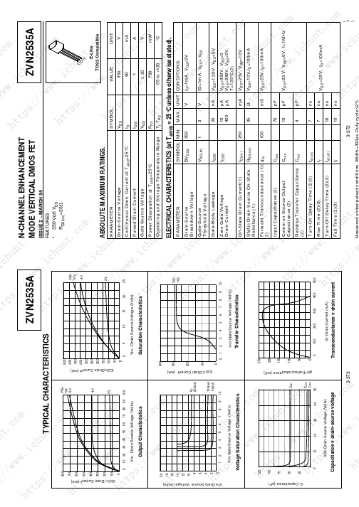
ZVN2535A
TYPICAL CHARACTERISTICS
800
VGS=
10V
700
6V
600
500
400
4V
300
200 3V
100
0 0 10 20 30 40 50 60 70 80 90 100
VDS - Drain Source Voltage (Volts)
Output Characteristics
Gate-Body Leakage
Zero Gate Voltage Drain Current
IGSS IDSS
20
nA VGS=± 20V, VDS=0V
10
µA VDS=350V, VGS=0
400 µA VDS=280V, VGS=0V,
T=125°C(2)
On-State Drain Current(1)
Input Capacitance (2)
Common Source Output Capacitance (2)
gfs-Transconductance (mS)
250 200 150 100
50
0
0
100
200
300
400
500
ID- Drain Current (mA)
Transconductance v drain current
3-373
N-CHANNEL ENHANCEMENT
MODE VERTICAL DMOS FET
ISSUE 2 – MARCH 94 FEATURES * 350 Volt VDS
RDS(on)=35Ω
ZVN2535A
电工电子技术常用半导体器件

7.2 半导体二极管
14
7.2.1 半导体二极管的结构
半导体二极管实际上是由一个PN结加上电极引线与外壳制成的,在PN结的P 区和N区分别用引线引出,P区的引线称为阳极(或正极),N区的引线称为阴极 (或负极),将PN结用外壳封装起来,便构成了晶体二极管,其结构和图形符号 如图7.7所示。二极管文字符号用字母VD表示,图形符号中箭头所指的方向是正 向导通的方向。
7.2 半导体二极管
22
图7.10 稳压二极管符号和伏安特性曲线
7.2 半导体二极管
23
(2)稳压二极管的主要参数 1)稳压电压UZ。UZ是稳压二极管反向击穿后的稳定工作电压值,如稳 压二极管2CW1的稳定电压是7~8.5V。由于制造工艺不易控制,同一型号的 稳压二极管,稳定电压值也会有一定范围的差异。但对每一只管子来说, 对应于一定的工作电流却有一个确定的稳定电压值。 2)稳定电流IZ。IZ是工作电压等于稳定电压时的工作电流,是稳压二 极管工作时的电流值。如上图7.11中A、B间是IZ正常的工作范围ΔIZ,ΔIZ 不大,稳压作用有限。应用时不要超过最大耗散功率,IZ偏大,稳定性可以 高一些,但功率消耗也大一些。 3)最大耗散功率PM。PM定义为管子不致产生热击穿的最大功率损耗, 即PM=UZ·IZM。根据PM和UZ可以推算出最大稳定电流IZM=PM/UZ。
7.2 半导体二极管
17
图7.9 二极管的伏安特性曲线
7.2 半导体二极管
18
1.正向偏置时的特性
当二极管的正极加高电位、负极加低电位时,称为二极管正向偏置, 此时二极管就产生正向电流,但当正向电压较小时,外电场不足以克服结 内电场对载流子扩散运动造成的阻力,这时正向电流很小,二极管呈现较 大的电阻,通常称这个区域为死区。
常用电子元件器件系列知识-三极管
电子元器件系列知识--三极管晶体三极管的结构和类型晶体三极管,是半导体基本元器件之一,具有电流放大作用,是电子电路的核心元件。
三极管是在一块半导体基片上制作两个相距很近的PN结,两个PN结把正块半导体分成三部分,中间部分是基区,两侧部分是发射区和集电区,排列方式有PNP和NPN两种,如图从三个区引出相应的电极,分别为基极b发射极e和集电极c。
发射区和基区之间的PN结叫发射结,集电区和基区之间的PN结叫集电极。
基区很薄,而发射区较厚,杂质浓度大,PNP型三极管发射区"发射"的是空穴,其移动方向与电流方向一致,故发射极箭头向里;NPN型三极管发射区"发射"的是自由电子,其移动方向与电流方向相反,故发射极箭头向外。
发射极箭头向外。
发射极箭头指向也是PN结在正向电压下的导通方向。
硅晶体三极管和锗晶体三极管都有PNP型和NPN型两种类型。
三极管的封装形式和管脚识别常用三极管的封装形式有金属封装和塑料封装两大类,引脚的排列方式具有一定的规律,如图对于小功率金属封装三极管,按图示底视图位置放置,使三个引脚构成等腰三角形的顶点上,从左向右依次为e b c;对于中小功率塑料三极管按图使其平面朝向自己,三个引脚朝下放置,则从左到右依次为e b c。
目前,国内各种类型的晶体三极管有许多种,管脚的排列不尽相同,在使用中不确定管脚排列的三极管,必须进行测量确定各管脚正确的位置,或查找晶体管使用手册,明确三极管的特性及相应的技术参数和资料。
晶体三极管的电流放大作用晶体三极管具有电流放大作用,其实质是三极管能以基极电流微小的变化量来控制集电极电流较大的变化量。
这是三极管最基本的和最重要的特性。
我们将ΔIc/ΔIb的比值称为晶体三极管的电流放大倍数,用符号“β”表示。
电流放大倍数对于某一只三极管来说是一个定值,但随着三极管工作时基极电流的变化也会有一定的改变。
晶体三极管的三种工作状态截止状态:当加在三极管发射结的电压小于PN结的导通电压,基极电流为零,集电极电流和发射极电流都为零,三极管这时失去了电流放大作用,集电极和发射极之间相当于开关的断开状态,我们称三极管处于截止状态。
- 1、下载文档前请自行甄别文档内容的完整性,平台不提供额外的编辑、内容补充、找答案等附加服务。
- 2、"仅部分预览"的文档,不可在线预览部分如存在完整性等问题,可反馈申请退款(可完整预览的文档不适用该条件!)。
- 3、如文档侵犯您的权益,请联系客服反馈,我们会尽快为您处理(人工客服工作时间:9:00-18:30)。
常用电子元器件参考资料第一节局部电气图形符号图形符号一.电阻器、电容器、电感器和变压器名称与说明图形符号名称与说明电感器、线圈、绕组或扼电阻器一般符号流图。
注:符号中半圆数不得少于3 个可变电阻器或可调电阻器滑动触点电位器带磁芯、铁芯的电感器带磁芯连续可调的电感器极性电容双绕组变压器注:可增加绕组数目可变电容器或可调电容器绕组间有屏蔽的双绕组变压器注:可增加绕组数目双联同调可变电容器。
注:可增加同调联数在一个绕组上有抽头的变压器微调电容器二.半导体管三.其它电气图形符号图形符号名称与说明具有两个电极的 压 电 晶 体注:电极数目可增加 图形符号 名称与说明或 接机壳或底板熔断器导线的连接指示灯及信号 灯 导线的不连接扬声器动合(常开)触点开 关蜂鸣器动断(常闭)触点开 关 接大地手动开关图形符号名称与说明 图形符号(1)二极管的符号(2)发光二极管名称与说明 JFET 结型场效应管 (1) N 沟道 (2) P 沟道PNP 型晶体三极管光电二极管稳压二极管NPN 型晶体三极 管全波桥式整流器变容二极管第一局部:主称 其次局部:材料符符第三局部:特征分类意义第四局部:序号符 对主称、材料一样,仅性能指标、尺寸大小有差异,但根本不影响互换使用的产品,赐予同一序号;假设性能指标、尺寸大小明 显影 响互 换时,则在序号后面用大写字母作其次节 常用电子元器件型号命名法及主要技术参数一.电阻器和电位器1. 电阻器和电位器的型号命名方法表 1 电阻器型号命名方法号 意义 号 意义 号 电阻器 电位器 R 电阻器 T 碳膜 1 一般 一般 W 电位器 H 合成膜 2 一般 一般 S 有机实芯 3 超高频 ―― N 无机实芯 4 高阻 ―― J 金属膜 5 高温 ―― Y 氧化膜 6 ―― ―― C 沉积膜 7 周密 周密 I 玻璃釉膜 8 高压 特别函数 P 硼碳膜 9 特别 特别 U 硅碳膜 G 高功率 ―― X 线绕 T 可调 ―― M 压敏 W ―― 微调 G 光敏 D ―― 多圈 R 热敏 B 温度补偿用 ―― C 温度测量用 ―― P 旁热式 ―― W 稳压式 ―― Z正温度系数 ――例如:(1) 周密金属膜电阻器 R J 7 3(2) 多圈线绕电位器 W X D 3第四局部:序号第三局部:类别〔周密〕 其次局部:材料〔金属膜〕 第一局部:主称〔电阻器〕第四局部:序号 第三局部:类别〔多圈〕 其次局部:材料〔线绕〕 第一局部:主称〔电位器〕名称 额定功率〔W 〕标称值系列精度 电阻器〔 〕、电位器〔 〕、电容器标称值〔PF 〕 2. 电阻器的主要技术指标(1) 额定功率电阻器在电路中长时间连续工作不损坏,或不显著转变其性能所允许消耗的最大功率称 为电阻器的额定功率。
电阻器的额定功率并不是电阻器在电路中工作时确定要消耗的功率, 而是电阻器在电路工作中所允许消耗的最大功率。
不同类型的电阻具有不同系列的额定功 率,如表 2 所示。
表 2 电阻器的功率等级实芯电阻器 0.25 0.5 1 2 5-0.5 1 2 6 10 15 线绕电阻器 25 35 50 75 100 1500.025 0.05 0.125 0.25 0.5 1 薄膜电阻器 25 10 2550 100(2) 标称阻值阻值是电阻的主要参数之一,不同类型的电阻,阻值范围不同,不同精度的电阻其阻值系列亦不同。
依据国家标准,常用的标称电阻值系列如表3 所示。
E24、E12 和 E6 系列也适用于电位器和电容器。
表 3 标称值系列1.0 1.1 1.2 1.3 1.5 1.6 1.82.0 E24±5%2.2 2.4 2.73.0 3.3 3.6 3.94.34.75.1 5.66.2 6.87.58.29.11.0 1.2 1.5 1.82.2 2.7E12 ±10% 3.3 3.9 4.7 5.6 6.8 8.2 - - E6±20%1.0 1.52.23.34.7 6.8 8.2 -表中数值再乘以 10n ,其中 n 为正整数或负整数。
(3) 允许误差等级 表 4 电阻的精度等级允许误差(%)±0.001等级符号允许误差(%) 等级符号±0.002 ±0.005 ±0.01±0.02 ±0.05 ±0.13. 电阻器的标志内容及方法(1) 文字符号直标法:用阿拉伯数字和文字符号两者有规律的组合来表示标称阻值,额 定功率、允许误差等级等。
符号前面的数字表示整数阻值,后面的数字依次表示第一位小数阻值和其次位小数阻值,其文字符号所表示的单位如表 5 所示。
如 1R5 表示 1.5Ω,2K7 表示 2.7k Ω, 表5文字符号 R 表示单位欧姆(Ω)K M GT千欧姆(103Ω) 兆欧姆(106Ω) 千兆欧姆(109Ω)兆兆欧姆(1012Ω)E X Y H U W B ±0.2 ±0.5 ±1 ±2 ±5 ±10 ±20 C D FG J 〔I 〕 K 〔II 〕 M 〔III 〕颜色第一位有效值其次位有效值倍率允许偏差100101102103104105106107108109 10-1 10-2 ―20% ~ +50%±5%±10%±20%例如:RJ71-0.125-5k1-II允许误差±10%标称阻值(5.1kΩ)额定功率1/8W型号由标号可知,它是周密金属膜电阻器,额定功率为1/8W,标称阻值为5.1kΩ,允许误差为±10%。
(2)色标法:色标法是将电阻器的类别及主要技术参数的数值用颜色〔色环或色点〕标注在它的外外表上。
色标电阻〔色环电阻〕器可分为三环、四环、五环三种标法。
其含义如图1 和图2 所示。
标称值第一位有效数字标称值其次位有效数字标称值有效数字后0 的个数允许误差黑00棕11红22橙33黄44绿55蓝66紫77灰88白金银无色99图1 两位有效数字阻值的色环表示法三色环电阻器的色环表示标称电阻值〔允许误差均为±20%〕。
例如,色环为棕黑红,表示10⨯102=1.0kΩ±20%的电阻器。
四色环电阻器的色环表示标称值〔二位有效数字〕及精度。
例如,色环为棕绿橙金表示15⨯103=15kΩ±5%的电阻器。
五色环电阻器的色环表示标称值〔三位有效数字〕及精度。
例如,色环为红紫绿黄棕表示275⨯104=2.75MΩ±1%的电阻器。
标称值第一位有效数字标称值其次位有效数字标称值第三位有效数字标称值有效数字后0 的个数允许误差倍100 101 102 103 104 105 106 107 108 109率允许偏差±1%±2%±0.5%±0.25±0.1%金银10-1 10-2一般四色环和五色环电阻器表示允许误差的色环的特点是该环离其它环的距离较远。
较标准的表示应是表示允许误差的色环的宽度是其它色环的〔1.5~2〕倍。
有些色环电阻器由于厂家生产不标准,无法用上面的特征推断,这时只能借助万用表推断。
颜色第一位有效值其次位有效值第三位有效值黑000棕111红222橙333黄444绿555蓝666紫777灰888白999图2 三位有效数字阻值的色环表示法4.电位器的主要技术指标(1)额定功率电位器的两个固定端上允许耗散的最大功率为电位器的额定功率。
使用中应留意额定功率不等于中心抽头与固定端的功率。
(2)标称阻值标在产品上的名义阻值,其系列与电阻的系列类似。
(3)允许误差等级实测阻值与标称阻值误差范围依据不同精度等级可允许±20%、±10%、±5%、±2%、±1% 的误差。
周密电位器的精度可达±0.1%。
(4)阻值变化规律指阻值随滑动片触点旋转角度〔或滑动行程〕之间的变化关系,这种变化关系可以是任何函数形式,常用的有直线式、对数式和反转对数式〔指数式〕。
第一局部:主称符号意义其次局部:材料符意义符第三局部:特征、分类意义第四局部:序号电容器对主称、材料一样,仅尺寸、性能指标略有不同,但根本不影响互使用的产品,赐予同一序号;假设尺寸性能指标的差异明显;影响互换使用时,则在序号后面用大写字母作为区在使用中,直线式电位器适合于作分压器;反转对数式〔指数式〕电位器适合于作收音机、录音机、电唱机、电视机中的音量把握器。
修理时假设找不到同类品,可用直线式代替,但不宜用对数式代替。
对数式电位器只适合于作音调把握等。
5.电位器的一般标志方法WT-2 3.3k ±10%允许误差±10%标称阻值3.3kΩ额定功率2W碳膜电位器WX-1 510ΩJ允许误差±5%标称阻值510Ω额定功率1W线绕电位器二.电容器1.电容器型号命名法表6 电容器型号命名法号号瓷介云母玻璃电解其他C瓷介1圆片非密封-箔式非密封Y云母2管形非密封-箔式非密封I玻璃釉3迭片密封-烧结粉固体密封O玻璃膜4独石密封-烧结粉固体密封Z纸介5穿心---穿心J金属化纸6支柱----B聚苯乙烯7---无极性-L涤纶8高压高压--高压Q漆膜9---特别特别S聚碳酸脂J金属膜H复合介质W微调D铝A钽N铌G合金T钛E其他例如:(1)铝电解电容器C D 1 1(2) 圆片形瓷介电容器C C 1-1(3) 纸介金属膜电容器C Z J X2. 电容器的主要技术指标第四局部:序号第三局部:特征分类〔箔式〕 其次局部:材料〔铝〕 第一局部:主称〔电容器〕第四局部:序号第三局部:特征分类〔圆片〕 其次局部:材料〔瓷介质〕 第一局部:主称〔电容器〕第四局部:序号第三局部:特征分类〔金属膜〕 其次局部:材料〔纸介〕 第一局部:主称〔电容器〕(1) 电容器的耐压: 常用固定式电容的直流工作电压系列为:6.3V ,10V ,16V ,25V , 40V ,63V ,100V ,160V ,250V ,400V 。
(2) 电容器容许误差等级:常见的有七个等级如表7 所示。
表 7+20% +50% +100% 容许误差 ±2% ±5% ±10% ±20% -30% -20% -10% 级别 0.2 I II IIIIV V VI♦電容常用字母代表誤差﹕ B: ±0.1﹪,C: ±0.25﹪,D: ±0.5﹪,F: ±1﹪,G: ±2 ﹪,J: ±5﹪,K: ±10﹪,M: ±20﹪,N: ±30﹪,Z:+80﹪-20﹪。