Samyoung_ARV规格书
DSS34二极管规格书(常州星海)

DSS32 THRU DSS310SURFACE MOUNT SCHOTTKY BARRIER RECTIFIERReverse Voltage - 20 to 100 Volts Forward Current - 3.0 AmpereCase : JEDEC SOD-123FL molded plastic bodyTerminals : Plated axial leads, solderable per MIL-STD-750,Method 2026Polarity : Color band denotes cathode end Mounting Position : AnyWeight :0.0007 ounce, 0.02 gramsFEATURESMECHANICAL DATAMAXIMUM RATINGS AND ELECTRICAL CHARACTERISTICSRatings at 25 C ambient temperature unless otherwise specified.Single phase half-wave 60Hz,resistive or inductive load,for capacitive load current derate by 20%.The plastic package carries Underwriters Laboratory Flammability Classification 94V-0Metal silicon junction,majority carrier conduction Low power loss,high efficiencyHigh forward surge current capability High temperature soldering guaranteed:250 C/10 seconds,0.375”(9.5mm) lead length,5 lbs. (2.3kg) tensionDSS32D32SYMBOLS UNITS DSS310D310201420V RRM V RMS V DC I (AV)I FSM V F 3.080.00.70Operating junction temperature range Maximum repetitive peak reverse voltage Maximum RMS voltageMaximum DC blocking voltageMaximum average forward rectified current Peak forward surge current8.3ms single half sine-wave superimposed on rated load (JEDEC Method)Maximum instantaneous forward voltage at 3.0A Maximum DC reverse current T A =25 C at rated DC blocking voltage T A =100 C I R 0.5T J T STGStorage temperature rangeDSS33D33DSS35D35DSS34D34DSS36D36DSS38D38DSS37D37DSS39D3*******40284050355060426080568010070100704970906390VOLTS VOLTS VOLTS Amp AmpsVolts C mA C-65 to +150-65 to +125-65 to +15020.010.00.550.850.52SOD-123FLDimensions in millimetersRATINGS AND CHARACTERISTIC CURVES DSS32 THRU DSS3100.2 0.4 0.6 0.8 1.0 1.1FIG. 3-TYPICAL INSTANTANEOUS FORWARDCHARACTERISTICSNUMBER OF CYCLES AT 60 HzFIG. 2-MAXIMUM NON-REPETITIVE PEAK FORWARDFIG. 1- FORWARD CURRENT DERATING CURVEA V E RA G E F O R W A R D R E C T I F I E D C U R R E N T ,A M P E R E SI N S T A N T A N E O U S F O R W A R D C U R R E N T ,A M P E R E SP E A K F O R W A R D S U R G E C U R R E N T ,A M P E R E SINSTANTANEOUS FORWARD VOLTAGE,VOLTS1001010.10.010.001PERCENT OF PEAK REVERSE VOLTAGE,%FIG. 4-TYPICAL REVERSE CHARACTERISTICSI N S T A N T A N E O U S R E V E R S E C U R R E N T ,M I L L I A M P E R E SAMBIENT TEMPERATURE, C【领先的片式无源器件整合供应商—南京南山半导体有限公司】 |样品申请单模板。
MEMORY存储芯片ADM708ARZ-REEL中文规格书

Data SheetADuM1410/ADuM1411/ADuM1412FEATURESLow power operation 5 V operation1.3 mA per channel maximum at 0 Mbps to 2 Mbps 4.0 mA per channel maximum at 10 Mbps 3 V operation0.8 mA per channel maximum at 0 Mbps to 2 Mbps 1.8 mA per channel maximum at 10 Mbps Bidirectional communication 3 V/5 V level translationHigh temperature operation: 105°C Up to 10 Mbps data rate (NRZ)Programmable default output stateHigh common-mode transient immunity: >25 kV/µs 16-lead, RoHS compliant, SOIC wide body package Safety and regulatory approvalsUL recognition: 3750 V rms for 1 minute per UL 1577 CSA Component Acceptance Notice 5A VDE certificate of conformityDIN V VDE V 0884-10 (VDE V 0884-10): 2006-12 V IORM = 560 V peakTÜV approval: IEC/EN 60950-1V GND V V V V GND DD22OA OB OC OD2206580-001Figure 1. ADuM1410V GND V V V V CTRL GND DD22OA OB OC ID2206580-002Figure 2. ADuM1411V GND V V V V CTRL GNDDD22OA OB IC ID 2206580-003APPLICATIONSGeneral-purpose multichannel isolation SPI interface/data converter isolation RS-232/RS-422/RS-485 transceivers Industrial field bus isolationGENERAL DESCRIPTIONThe ADuM1410/ADuM1411/ADuM14121 are four-channel digital isolators based on Analog Devices, Inc., i Coupler® technology. Combining high speed CMOS and monolithic air core transformer technologies, these isolation components provide outstanding performance characteristics superior to alternatives such as optocoupler devices.By avoiding the use of LEDs and photodiodes, i Coupler devices remove the design difficulties commonly associated with opto-couplers. The usual concerns that arise with optocouplers, such as uncertain current transfer ratios, nonlinear transfer functions, and temperature and lifetime effects, are eliminated with the simple i Coupler digital interfaces and stable performance characteristics. The need for external drivers and other discrete components is eliminated with these i Coupler products. Furthermore, i Coupler1Protected by U.S. Patents 5,952,849; 6,873,065; 6,903,578; and 7,075,329.Figure 3. ADuM1412devices consume one-tenth to one-sixth the power of optocou-plers at comparable signal data rates.The ADuM1410/ADuM1411/ADuM1412 isolators provide four independent isolation channels in a variety of channel configu-rations and data rates (see the Ordering Guide) up to 10 Mbps. All models operate with the supply voltage on either side ranging from 2.7 V to 5.5 V , providing compatibility with lower voltage systems as well as enabling voltage translation functionality across the isolation barrier. All products also have a default output control pin. This allows the user to define the logic state the outputs are to adopt in the absence of the input power. Unlike other optocoupler alternatives, the ADuM1410/ADuM1411/ ADuM1412 isolators have a patented refresh feature that ensures dc correctness in the absence of input logic transitions and during power-up/power-down conditions.Data Sheet ADuM1410/ADuM1411/ADuM1412 SPECIFICATIONSELECTRICAL CHARACTERISTICS—5 V OPERATION4.5 V ≤ V DD1 ≤5.5 V, 4.5 V ≤ V DD2 ≤ 5.5 V; all minimum/maximum specifications apply over the entire recommended operation range, unless otherwise noted; all typical specifications are at T A = 25°C, V DD1 = V DD2 = 5 V. All voltages are relative to their respective ground. Table 1.Parameter Symbol Min Typ Max Unit Test Conditions/CommentsDC SPECIFICATIONSInput Supply Current per Channel,QuiescentI DDI (Q)0.50 0.73 mAOutput Supply Current per Channel,QuiescentI DDO (Q)0.38 0.53 mAADuM1410, Total Supply Current,Four Channels1DC to 2 MbpsV DD1 Supply Current I DD1 (Q) 2.4 3.2 mA DC to 1 MHz logic signal frequency V DD2 Supply Current I DD2 (Q) 1.2 1.6 mA DC to 1 MHz logic signal frequency10 Mbps (BRWZ Version Only)V DD1 Supply Current I DD1 (10)8.8 12 mA 5 MHz logic signal frequency V DD2 Supply Current I DD2 (10) 2.8 4.0 mA 5 MHz logic signal frequency ADuM1411, Total Supply Current,Four Channels1DC to 2 MbpsV DD1 Supply Current I DD1 (Q) 2.2 2.8 mA DC to 1 MHz logic signal frequency V DD2 Supply Current I DD2 (Q) 1.8 2.4 mA DC to 1 MHz logic signal frequency10 Mbps (BRWZ Version Only)V DD1 Supply Current I DD1 (10) 5.4 7.6 mA 5 MHz logic signal frequency V DD2 Supply Current I DD2 (10) 3.8 5.3 mA 5 MHz logic signal frequency ADuM1412, Total Supply Current,Four Channels1DC to 2 MbpsV DD1 or V DD2 Supply Current I DD1 (Q), I DD2(Q)2.0 2.6 mA DC to 1 MHz logic signal frequency10 Mbps (BRWZ Version Only)V DD1 or V DD2 Supply Current I DD1 (10), I DD2 (10) 4.6 6.5 mA 5 MHz logic signal frequencyAll ModelsInput Currents I IA, I IB, I IC,I ID, I CTRL1,I CTRL2, I DISABLE −10 +0.01 +10µA 0 V ≤ V IA, V IB, V IC, V ID ≤ V DD1 or V DD2,0 V ≤ V CTRL1, V CTRL2 ≤ V DD1 or V DD2,0 V ≤ V DISABLE ≤ V DD1Logic High Input Threshold V IH 2.0 V Logic Low Input Threshold V IL 0.8 VLogic High Output Voltages V OAH, V OBH,V OCH, V ODH (V DD1 or V DD2) − 0.1 5.0 V I Ox = −20 µA, V Ix = V IxH (V DD1 or V DD2) − 0.4 4.8 V I Ox = −4 mA, V Ix = V IxHLogic Low Output Voltages V OAL, V OBL,V OCL, V ODL0.0 0.1 V I Ox = 20 µA, V Ix = V IxL0.04 0.1 V I Ox = 400 µA, V Ix = V IxL0.2 0.4 V I Ox = 4 mA, V Ix = V IxL Rev. M | Page of 22ADuM1410/ADuM1411/ADuM1412 Data Sheet Parameter Symbol Min Typ Max Unit Test Conditions/Comments SWITCHING SPECIFICATIONSADuM1410ARWZ/ADuM1411ARWZ/ADuM1412ARWZMinimum Pulse Width2PW 1000 ns C L = 15 pF, CMOS signal levels Maximum Data Rate3 1 Mbps C L = 15 pF, CMOS signal levels Propagation Delay4t PHL, t PLH20 65 100 ns C L = 15 pF, CMOS signal levels Pulse Width Distortion, |t PLH − t PHL|4 PWD 40 ns C L = 15 pF, CMOS signal levels Propagation Delay Skew5t PSK50 ns C L = 15 pF, CMOS signal levels Channel-to-Channel Matching6t PSKCD/OD50 ns C L = 15 pF, CMOS signal levels ADuM1410BRWZ/ADuM1411BRWZ/ADuM1412BRWZMinimum Pulse Width2PW 100 ns C L = 15 pF, CMOS signal levels Maximum Data Rate310 Mbps C L = 15 pF, CMOS signal levels Propagation Delay4t PHL, t PLH20 30 50 ns C L = 15 pF, CMOS signal levels Pulse Width Distortion, |t PLH − t PHL|4 PWD 5 ns C L = 15 pF, CMOS signal levels Change vs. Temperature 5 ps/°C C L = 15 pF, CMOS signal levels Propagation Delay Skew5t PSK30 ns C L = 15 pF, CMOS signal levels Channel-to-Channel Matching,Codirectional Channels6t PSKCD 5 ns C L = 15 pF, CMOS signal levelsChannel-to-Channel Matching,Opposing-Directional Channels6t PSKOD 6 ns C L = 15 pF, CMOS signal levelsAll ModelsOutput Rise/Fall Time (10% to 90%) t R/t F 2.5 ns C L = 15 pF, CMOS signal levelsCommon-Mode Transient Immunity at Logic High Output7|CM H| 25 35 kV/µs V Ix = V DD1 or V DD2, V CM = 1000 V,transient magnitude = 800 VCommon-Mode Transient Immunity at Logic Low Output7 |CM L| 25 35 kV/µs V Ix = 0 V, V CM = 1000 V,transient magnitude = 800 VRefresh Rate f r 1.2 MbpsInput Enable Time8t ENABLE 2.0 µs V IA, V IB, V IC, V ID = 0 V or V DD1 Input Disable Time8t DISABLE 5.0 µs V IA, V IB, V IC, V ID = 0 V or V DD1Input Dynamic Supply Current per Channel9I DDI (D)0.12 mA/MbpsOutput Dynamic Supply Current per Channel9I DDO (D)0.04 mA/Mbps1 The supply current values for all four channels are combined when running at identical data rates. Output supply current values are specified with no output load present. The supply current associated with an individual channel operating at a given data rate can be calculated as described in the Power Consumption section. See Figure 8 through Figure 10 for information on per-channel supply current as a function of data rate for unloaded and loaded conditions. See Figure 11 through Figure 15 for total V DD1 and V DD2 supply currents as a function of data rate for ADuM1410/ADuM1411/ADuM1412 channel configurations.2 The minimum pulse width is the shortest pulse width at which the specified pulse width distortion is guaranteed.3 The maximum data rate is the fastest data rate at which the specified pulse width distortion is guaranteed.4 t PHL propagation delay is measured from the 50% level of the falling edge of the V Ix signal to the 50% level of the falling edge of the V Ox signal. t PLH propagation delay is measured from the 50% level of the rising edge of the V Ix signal to the 50% level of the rising edge of the V Ox signal.5 t PSK is the magnitude of the worst-case difference in t PHL or t PLH that is measured between units at the same operating temperature, supply voltages, and output load within the recommended operating conditions.6 Codirectional channel-to-channel matching is the absolute value of the difference in propagation delays between any two channels with inputs on the same side of the isolation barrier. Opposing-directional channel-to-channel matching is the absolute value of the difference in propagation delays between any two channels with inputs on opposing sides of the isolation barrier.7 |CM H| is the maximum common-mode voltage slew rate that can be sustained while maintaining V O > 0.8 V DD2. |CM L| is the maximum common-mode voltage slew rate that can be sustained while maintaining V O < 0.8 V. The common-mode voltage slew rates apply to both rising and falling common-mode voltage edges. The transient magnitude is the range over which the common mode is slewed.8 Input enable time is the duration from when V DISABLE is set low until the output states are guaranteed to match the input states in the absence of any input data logic transitions. If an input data logic transition within a given channel does occur within this time interval, the output of that channel reaches the correct state within the much shorter duration as determined by the propagation delay specifications within this data sheet. Input disable time is the duration from when V DISABLE is set high until the output states are guaranteed to reach their programmed output levels, as determined by the CTRL2 logic state (see Table 14).9 Dynamic supply current is the incremental amount of supply current required for a 1 Mbps increase in signal data rate. See Figure 8 through Figure 10 for information on per-channel supply current for unloaded and loaded conditions. See the Power Consumption section for guidance on calculating the per-channel supply current for a given data rate.Rev. M | Page of 22Data Sheet ADuM1410/ADuM1411/ADuM1412ELECTRICAL CHARACTERISTICS—3 V OPERATION2.7 V ≤ V DD1 ≤3.6 V, 2.7 V ≤ V DD2 ≤ 3.6 V; all minimum/maximum specifications apply over the entire recommended operation range, unless otherwise noted; all typical specifications are at T A = 25°C, V DD1 = V DD2 = 3.0 V. All voltages are relative to their respective ground. Table 2.Parameter Symbol Min Typ Max Unit Test Conditions/CommentsDC SPECIFICATIONSInput Supply Current per Channel,QuiescentI DDI (Q)0.25 0.38 mAOutput Supply Current per Channel,QuiescentI DDO (Q)0.19 0.33 mAADuM1410, Total Supply Current,Four Channels1DC to 2 MbpsV DD1 Supply Current I DD1 (Q) 1.2 1.6 mA DC to 1 MHz logic signalfrequency V DD2 Supply Current I DD2 (Q)0.8 1.0 mA DC to 1 MHz logic signalfrequency10 Mbps (BRWZ Version Only)V DD1 Supply Current I DD1 (10) 4.5 6.5 mA 5 MHz logic signal frequency V DD2 Supply Current I DD2 (10) 1.4 1.8 mA 5 MHz logic signal frequency ADuM1411, Total Supply Current,Four Channels1DC to 2 MbpsV DD1 Supply Current I DD1 (Q) 1.0 1.9 mA DC to 1 MHz logic signal frequency V DD2 Supply Current I DD2 (Q)0.9 1.7 mA DC to 1 MHz logic signal frequency10 Mbps (BRWZ Version Only)V DD1 Supply Current I DD1 (10) 3.1 4.5 mA 5 MHz logic signal frequency V DD2 Supply Current I DD2 (10) 2.1 3.0 mA 5 MHz logic signal frequency ADuM1412, Total Supply Current,Four Channels1DC to 2 MbpsV DD1 or V DD2 Supply Current I DD1 (Q), I DD2 (Q) 1.0 1.8 mA DC to 1 MHz logic signal frequency10 Mbps (BRWZ Version Only)V DD1 or V DD2 Supply Current I DD1 (10), I DD2 (10) 2.6 3.8 mA 5 MHz logic signal frequencyAll ModelsInput Currents I IA, I IB, I IC, I ID,I CTRL1,I CTRL2, I DISABLE −10 +0.01 +10µA 0 V ≤ V IA, V IB, V IC, V ID ≤ V DD1 or V DD2,0 V ≤ V CTRL1, V CTRL2 ≤ V DD1 or V DD2,0 V ≤ V DISABLE ≤ V DD1Logic High Input Threshold V IH 1.6 V Logic Low Input Threshold V IL 0.4 VLogic High Output Voltages V OAH, V OBH,V OCH, V ODH (V DD1 or V DD2) − 0.1 3.0 V I Ox = −20 µA, V Ix = V IxH (V DD1 or V DD2) − 0.4 2.8 V I Ox = −4 mA, V Ix = V IxHLogic Low Output Voltages V OAL, V OBL,V OCL, V ODL0.0 0.1 V I Ox = 20 µA, V Ix = V IxL0.04 0.1 V I Ox = 400 µA, V Ix = V IxL0.2 0.4 V I Ox = 4 mA, V Ix = V IxL Rev. M | Page of 22ADuM1410/ADuM1411/ADuM1412 Data Sheet。
车载产品规格书(非常详尽的技术参数与指标)
产 品 规 格 书SPECIFICATION客户名称:CUSTOMER : 机种名称: DESCRIPTION : 车载DVD CAR DVD 机种型号: MODEL : DV-7610发行日期:ISSUE DATE : 2008.12.01一:范围Scope1.本产品规格书适用于华阳通用公司车用DVD系统,产品型号:DV-7610;产品代号:7600This specification is only suitable for FORYOU Car-DVD system (Model: DV-7610, Product Code: 7600 ).2.本产品规格书规定了DV-7610车用DVD系统的技术要求、试验方法、标志、标签、包装、运输及存储要求。
本规格书适用于设计定型与出货检验,在生产检验,定型检验和质量一致性检验时,作为质量鉴定检验的依据。
The specification prescribes product performance, technical parameters, testing method, and the items for label, package, storage and transportation. It can be used as the referenced standard for Quality Verification including Production Verification, Case-hardened Verification and Quality Conformity Verification.3.下列标准包含的条文,通过在本产品规格书中引用而构成为本产品规格书中的条文。
The entire referenced standard listed below will become a part of the DV-76 specification. 本规格书的引用标准 Referenced standard:3.1 GB-13837-1997 声音和电视广播接收机及有关设备无线电干扰特性限值和测量方法Limits and methods of measurement of interfere characteristics of audioand television broadcast receivers and associated equipment3.2 GB/T9384-1997 广播收音机、广播电视接收机、磁带录音机、声频功率放大器(收音机)的环境实验要求和试验方法Requirements and methods of Environmental test for Broadcastingreceiver, TV receiver, Cassette Recorder and Audio Amplifier3.3 GB4013-1995 数字音响技术术语Technology terms of Digital Audio system3.4 GB/T14860 激光唱机通用技术条件General Technology conditions of Video Compact Disc player3.5 IEC908-1987 CD数字音频系统CD Digital Audio System3.6 EIAJ CP-307 CD唱机测量方法CD Player Test Methods3.7 EIAJ CP-308 CD唱机用测试唱片CD Player Test Disc3.8 GB/T14277 音频组合设备通用技术条件General Technology conditions of Audio Associated Equipment3.9 GB9374-88 声音广播接收机基本参数Basic parameter of Audio broadcasting receiver3.10 GB2846-88 调幅广播收音机测量方法AM Tuner receivers test methods3.11 GB6163-85 调频广播接收机测量方法FM Tuner receivers test methods3.12 GB9883-88 广播接收机及有关设备的传导抗扰度特性测量方法Limits and methods of measurement of immunity characteristicsof sound and television broadcast receivers and associatedequipment3.13 Publication315 收音接收机设备的测试方法Tuner receivers equipments test methods3.14 SJ/T10730-1997 VCD视盘机通用技术规范General specification for Video Compact Disc player3.15 DVD视盘机通用技术规范General specification for Digital Video Disc player3.16GB/T xxxx-xxxx 液晶显示器测量方法Measurement method for TFT display equipment3.17GB xxxx-xxxx 液晶数字电视广播接收机通用技术规范General specification for TFT-LCD digital TV receiver二:基本功能描述Basic function description1、DVD功能 DVD function1.1 支持碟片格式 Support DISC type12cm DVD-Video (DVD-5/9/10/18), DVD±R/RW, DVD-ROM ,CD-R/RW, CD-DA, VCD, SVCD, Photo CD, MP3/JPEG/MPEG三合一碟1.2 支持媒体格式 Support media typeMPEG I/II/IV, MP3, WMA, JPEG, DivX 、XviD1.3 选择字幕语言;选择菜单语言;选择音频语言Subtitle Language;Menu language;Audio language1.4 快进、快退;慢进,慢退模式;重复播放;扫描播放;随机播放;选择时间播放;图象缩放, 多角度选择,编程,步进和重复播放功能.Fast Forward, Fast Rewind, Slow Forward, Slow Rewind, Repeat Playback, Scanning Playback,Random Playback, Specific Time Playback, Zoom Image, Multi-Angle Supported, Programmable Playback, Step Forward Playback.1.5断点自动记忆功能Last Memory1.6 章节转换静音Mute between Chapters Changing1.7密码设置Password setting1.8 音频解码方式:192/96/48/44.1.f.s 24-bit 6Ch DACAudio decode mode: 192/96/48/44.1.f.s 24-bit 6Ch DAC1.9 OSD功能:普通OSD1.10 TV Guardian 功能(预留)TV Guardian function(option)1.11 动作时间Action time7.18.1 L oad→Start Play:≤15″7.18.2 Stop→Start Play:≤10″7.18.3 Short Access(Tr1→Tr2):≤2″7.18.4 Long Access(First Tr→Last Tr):≤5″7.18.5 Play→E jected:≤5″2、AM/FM 功能(全制式)AM/FM function (ALL)2.1手动动及自动搜索电台Manual Search Station & Auto Search Station2.2手动及自动存储电台Manual Store Station & Auto Store Station2.3 扫描存储电台Scan and store2.4 30个电台预置:5BAND*6;FM:3 BAND;2 BAND30 Preset Stations :3 FM Bands & 2 AM Bands, 6 stations per band2.5调入预设电台Loaded Preset Stations3、3G无线接入功能(可选)3G Wireless Access Function (Optional)3.1 多模接入HSUPA/HSDPA/UMTS/EDGE/GPRSMultimode AccessHSUPA/HSDPA/UMTS/EDGE/GPRS3.2 支持频段Frequency Support:HSPA/UMTS 850/1900/2100 MHzEDGE/GPRS 850/900/1800/1900 MHz3.3 速率VelocityHSUPA uplink up to 2.0 MbpsHSDPA downlink up to 7.2 MbpsWCDMA (UMTS) uplink data rate up to 384 kbpsEDGE data up to 237 Kbps DL and 118Kbps ULGPRS data up to 85.6 Kbps DL and 42.8 Kbps UL4、TFT 显示TFT display4.1 电动翻转结构,左右手动可调Motorlized flip up/down structure, also can be adjusted left/right by hand.4.2 屏幕显示分辨率 800(RGB)×480TFT resolution : 800(RGB)×4804.3 视频信号制式自动识别 (NTSC / PAL / SECAM)Auto identified for video signal’s type (NTSC / PAL / SECAM)4.4 屏幕显示效果调节 (亮度 / 对比度/ 色饱和度)User defined display effect (Brightness/Contrast/Color)4.5显示屏角度调节功能Adjustable Display Angle4.6防堵转功能Prevent from block4.7显示屏翻转位置记忆功能Position Memory5、LCD辅助显示LCD display on assistance5.1显示操作信息LCD:段码式,见效果图:Display mode in LCD: segment as below5.2显示模式:白背光,黑底白字Display Mode: white backlight, black ground with white words6、触摸屏控制功能Touch screen control7、内置导航,地图存储方式:外置SD卡。
GRACE-KRV 压敏电阻规格书

GRACE-KRV 压敏电阻规格书GRACECeramic transient voltage suppressorsSMD multilayer transient voltage suppressors, standard seriesSeries/Type:Date: November 20191 . Standard series① ② ③ ④ ⑤ ⑥ ⑦①production series:GRACE Varistor ②size :1206(3216)③varistor voltage tolerance:K: 10% ; L: 15% ; M: 20% ④working voltage (AC): 260:26V,4R0=4.0V⑤type : G: general ; E :ESD ; H :high energy ⑥end termination: S: Ag/Pd N: Ag/Ni/Sn ⑦package :T : taping B: bulk2 . SizeModelLength(L) Width(W) High(H) L10402(1005) 0603(1608) 0805(2019) 1206(3216) 1210(3225) 1812(4532)2220(5650) 3220(08CL) 4032(10CL) 4840(12CL) 1.00±0.20 0.50±0.20 0.50±0.20 0.30±0.201.60±0.20 0.80±0.20 0.80±0.20 0.30±0.202.00±0.20 1.20±0.20 0.80±0.20 0.40±0.203.20±0.20 1.60±0.20 1.20±0.20 0.40±0.303.20±0.20 2.50±0.20 1.20±0.20 0.40±0.304.50±0.20 3.20±0.20 1.30±0.20 0.50±0.305.60±0.20 5.00±0.20 1.50±0.20 0.80±0.308.00±0.30 5.00±0.30 2.00±0.30 0.80±0.3010.0±0.30 8.00±0.30 2.00±0.30 0.80±0.3012.0±0.30 10.0±0.30 2.50±0.30 2.50±0.303 . Electrical specifications and ordering codesType:0402~0805□ Leadless,size 0402~0805□ Multilayer ceramic construction□ Wide operating temperature :﹣55℃ to﹢125℃ □ Fast response(≤1ns)□ High transient current capability □ Low leakage currentWorking voltageGRACE AC DCPart numberV RMS (V) V DC (V)KRV0402M2R5ENT KRV0402M4R0ENT KRV0402M6R0ENT KRV0402L8R0ENT KRV0402L110ENT KRV0402L140ENT KRV0603M2R5GNT KRV0603M4R0GNT KRV0603M6R0GNT KRV0603L110GNT KRV0603K140ENT KRV0603K170ENT KRV0603K200ENT KRV0603K250ENT KRV0603K300ENT KRV0805M4R0GNT KRV0805M6R0GNT KRV0805L110GNT KRV0805L140GNT KRV0805K170GNT KRV0805K200GNT KRV0805K250GNT KRV0805K300GNT2.5 4 6 8 11 14 2.5 4 6 11 14 17 20 25 30 4 6 11 14 17 20 25 30Breakdown voltage @1mA DC V B (V)5 8 12 14 18 25 5 8 12 18 25 27 33 39 47 8 12 18 22 27 33 39 47±20% ±20% ±20% ±15% ±15% ±15% ±20% ±20% ±20% ±15% ±10% ±10%±10% ±10% ±10% ±20% ±20% ±15% ±15% ±10% ±10% ±10% ±10%PeakCapacitancevoltage energy current 8/20 μs 10/100μs 8/20μs @ 1kHz Vc(V)1015.5 25 35 45 58 10 15.5 25 35 52 58 65 72 81 15.5 25 35 45 58 65 72 81E T (J)0.02 0.02 0.05 0.05 0.05 0.05 0.10 0.10 0.10 0.10 0.20 0.20 0.20 0.20 0.20 0.10 0.10 0.10 0.20 0.20 0.20 0.20 0.20Ip(A)10 10 10 10 10 10 20 20 30 30 30 30 30 30 30 30 30 40 40 40 40 40 40C(pF)80 60 50 40 40 40 360 270 200 180 120 100 100 100 80 600 500 360 350 260 240 200 165Notes:1.Typical leakage at 25℃2.At normal:ΔCp±30%,In order to satisfy the applications of customer in various fields, the capacitance range can be designed during manufacturing according to the request, please contact our sales department if neededType:1206~1812□ Leadless,size 3216~4532□ Multilayer ceramic construction□ Wide operating temperature :﹣55℃ to﹢125℃ □ Fast response(≤1ns)□ High transient current capability □ Low leakage currentGRACEPart numberKRV1206M4R0GNT KRV1206K6R0GNT KRV1206K110GNT KRV1206L140GNT KRV1206K200GNT KRV1206K250GNT KRV1206K300GNT KRV1206M350GNT KRV1210M4R0GNT KRV1210M6R0GNT KRV1210L110GNT KRV1210L140GNT KRV1210L170GNT KRV1210L200GNT KRV1210L250GNT KRV1210K300GNT KRV1210K350GNT KRV1210K400GNT KRV1210K600GNT KRV1812K200GNT KRV1812K250GNT KRV1812K300GNT KRV1812K350GNT KRV1812K400GNT KRV1812K600GNT KRV1812K750GNTNotes:Working voltage ACDCBreakdown Clamping Capacitancevoltage voltage energy current @1mA DC 8/20 μs 1A 10/100μs 8/20μs @1kHz V B (V)8 12 18 22 33 39 47 56 8 12 18 22 27 33 39 47 56 68 100 33 39 47 56 68 100 120±20% ±10% ±10% ±15% ±10% ±10% ±10% ±20% ±20% ±20% ±15% ±15%±15% ±15% ±15% ±10% ±10% ±10% ±10% ±10% ±10% ±10% ±10% ±10% ±10% ±10%V RMS (V) V DC (V)4 6 11 14 20 25 30 35 46 11 14 17 20 25 30 35 40 60 20 25 30 35 40 60 755.6 8 14 18 26 31 38 45 5.6 8 14 18 22 26 31 38 45 56 85 26 31 38 45 56 85 100Vc(V)15.5 25 35 45 65 72 81 110 15.5 25 35 45 58 65 72 81 110 120 165 45 55 77 77 120 160 250E T (J)0.02 0.02 0.02 0.02 0.20 0.20 0.50 0.50 0.50 0.50 1.00 1.00 1.00 1.00 1.001.002.00 2.00 2.50 1.00 1.00 1.00 1.00 2.00 2.00 2.50Ip(A)100 100 100 100 150 150 180 180 100 100 200 200 200 200 200 200 250 250 200 400 400 400 400 600 600 800C(pF)1200 900 720 550 380 360 300 220 1800 1300 1150 900 750 650 600 480 380 300 200 1300 1200 900 900 650 600 5001.Typical leakage at 25℃2.In order to satisfy the applications of customer in various fields, the capacitance range can be designed during manufacturingaccording to the request, please contact our sales department if needed。
AR9331模块规格书-4zx
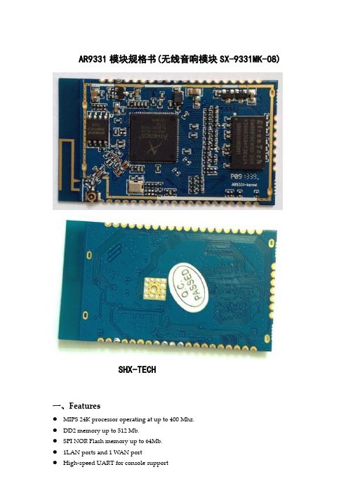
AR9331模块规格书(无线音响模块SX-9331MK-08)SHX-TECH一、Features● MIPS 24K processor operating at up to 400 Mhz.● DD2 memory up to 512 Mb.● SPI NOR Flash memory up to 64Mb.● 1LAN ports and 1 WAN port● High-speed UART for console support● I2S audio interface● USB 2.0 host/device mode support● GPIO/LED support● SPI support.二、Hardware Specifications芯片解决方案CPU:AR9331 RF:AR9331CPU主频400MHzDDR 64Mbyte DDR2闪存8Mbyte SPI FLASH遵循标准IEEE802.3u MDI / MDIX 10/100 快速以太网IEEE802.11b/g 无线LAN接口IEEE 802.11n 无线LAN标准网络接口LAN:1 x 10/100M Auto MDI/MDIX 插针接口WAN:1 x 10/100M Auto MDI/MDIX 插针接口(可以复用为LAN口)软件功能接口I2SUSB 2.0JTAGUART接口47PIN 邮标孔焊盘(PIN 间距为2.0mm)Data rate 11b: 11M, 5.5M, 2M, 1Mbps11g: 54M, 48M, 36M, 24M, 18M, 12M, 9M, 6Mbps11N:6.5M, 13M, 13.5M,19.5M, 26M,27M, 39M, 40.5M,52M, 54M,58.5M, 65M,81M,108M,121.5M,135M,150MbpsTransmission mode DSSSModulation OFDM/BPSK/QPSK/CCK/DQPSK/DBPSK Frequency Range 2412 MHz ~ 2472MHz(channel 1 ~ channel 13) 供电需求 3.3V,1APower consumption ≦3WRF Power @25℃(±2dB) 802.11b 19 ± 2dBm @EVM -20dBm802.11g 6-24Mbps 17 ± 2dBm36-48Mbps 16 ± 2dBm54Mbps 15± 2dBm @EVM -25dBm 802.11n HT20 MCS 7 14± 2dBm @EVM -28dBm HT40 MCS 7 14 ± 2dBm @EVM -28dBmReceiver sensitivity IEEE802.11b11Mbps≦-83dBmIEEE 802.11g54Mbps≦-70dBmIEEE 802.11nHT 20MCS 7≦-65dBmHT 40MCS 7≦-62dBm尺寸53.2*30MM环境Operating Temperature: -10℃~45℃Storage Temperature: -40℃~85℃Operating Humidity: 10%~90% non-condensingStorage Humidity: 10%~90% non-condensing 环保遵循RoHs标准三、Pin Description:四、Dimensions and Footprint:五、接口参考电路:1、以太网接口电路:2、LED指示灯电路:3、复位电路:。
MEMORY存储芯片MT29F256G08AUCABH3-10IT中文规格书

Figure 230: Differential Output Slew Rate DefinitionTR TF diffV OH,diff(AC)V OL,diff(AC)D i f f e r e n t i a l I n p u t V o l t a g e (D Q S _t , D Q S _c )Table 117: Differential Output Slew RateNote: 1.SR = slew rate; Q = query output; diff = differential signals.Reference Load for AC Timing and Output Slew RateThe effective reference load of 50Ω to V TT = V DDQ and driver impedance of R ZQ /7 for each output was used in defining the relevant AC timing parameters of the device as well as output slew rate measurements.R ON nominal of DQ, DQS_t and DQS_c drivers uses 34 ohms to specify the relevant AC timing parameter values of the device. The maximum DC high level of output signal =1.0 × V DDQ , the minimum DC low level of output signal = { 34 /( 34 + 50 ) } × V DDQ = 0.4 ×V DDQ .The nominal reference level of an output signal can be approximated by the following:The center of maximum DC high and minimum DC low = { ( 1 + 0.4 ) / 2 } × V DDQ = 0.7 ×V DDQ . The actual reference level of output signal might vary with driver R ON and refer-ence load tolerances. Thus, the actual reference level or midpoint of an output signal is at the widest part of the output signal’s eye.4Gb: x8, x16 Automotive DDR4 SDRAM Electrical Characteristics – AC and DC Output Measurement LevelsTable 143: I DD5R Measurement – Loop Pattern 1Notes:1.DQS_t, DQS_c are V DDQ .2.BG1 is a "Don't Care" for x16 devices.3.DQ signals are V DDQ .4.For x4 and x8 only.4Gb: x8, x16 Automotive DDR4 SDRAM Current Specifications – Patterns and Test Conditions。
A-35GB产品规格书
● 产品特性标准超薄产品,高度30mm-30~+70℃工作温度(具体查看降额曲线) 短路/过载/过压保护功能100%满载老化 效率高、高可靠性 2年质保期●应用领域:工业控制系统、机械与电气设备、电子仪器仪表、工业自动化、家用电器等● 参考标准EN55024\EN61000-4-2,3,4,5,6,8,11\GB17625.1\EN61000-3-2,-3\EN55022\GB4943\UL1012● 产品描述A-35GB 系列是一款35W 单路恒压输出的工业控制电源,电压输入范围176~264VAC ,输出电压有5V 、12V 、24V 等,可适用于工业控制系统、机械与电气设备、电子仪器仪表、工业自动化、家用电器等多种工业领域。
超高的效率,紧凑的外壳设计,良好的散热,保障了本系列产品可长期稳定的工作。
● 产品命名电气参数输出负载与温度曲线 静态特性曲线机构尺寸●安装方式●产品安装、使用说明:1、安装时,请按照安装方式说明进行安装。
2、在安装完毕通电试运行之前,请检查和校对各接线端子上的连线,确信输入和输出、交流和直流、正极和负极、电压值和电流值等正确,杜绝接反接错现象的发生,避免损坏电源和用户设备。
3、通电前请使用万用表测量火线、零线和接地线是否短路,输出端是否短路;通电时最好空载启动。
4、使用时请勿超过电源标称值,以免影响产品的可靠性。
如需更改电源的输出参数,请客户在使用电源前向本司技术部门咨询,以保证使用效果和可靠性。
5、为保证使用的安全性和减小干扰,请确保接地端可靠接地(接地线大于AWG18#)。
6、电源如出现故障,请勿擅自对其维修,请尽快与本司客户服务部联系,客服专线:86-519-85215050。
●运输、储存:1、运输:本包装适用与汽车、船、飞机、火车等运输,运输过程中应防雨,文明装卸。
2、储存:产品未使用时应放在包装箱里,储存环境温度和相对湿度应符合该产品的要求,仓库内不应有腐蚀性气体或产品,并且无强烈的机械振动、冲击和强磁场作用。
半导体传感器ADM4857ARZ中文规格书
ADuM1400/ADuM1401/ADuM1402 Data SheetELECTRICAL CHARACTERISTICS—MIXED 5 V/3 V OR 3 V/5 V, 105°C OPERATION15 V/3 V operation: 4.5 V ≤ V DD1 ≤ 5.5 V, 2.7 V ≤ V DD2 ≤ 3.6 V; 3 V/5 V operation: 2.7 V ≤ V DD1 ≤ 3.6 V, 4.5 V ≤ V DD2 ≤ 5.5 V; all minimum/maximum specifications apply over the entire recommended operation range, unless otherwise noted; all typical specifications are at T A = 25°C; V DD1 = 3.0 V, V DD2 = 5 V or V DD1 = 5 V, V DD2 = 3.0 V. These specifications do not apply to ADuM1400W, ADuM1401W, and ADuM1402W automotive grade versions.Table 3.Parameter Symbol Min Typ Max Unit Test ConditionsDC SPECIFICATIONSInput Supply Current per Channel, Quiescent I DDI (Q)5 V/3 V Operation 0.50 0.53 mA3 V/5 V Operation 0.26 0.31 mAOutput Supply Current per Channel, Quiescent I DDO (Q)5 V/3 V Operation 0.11 0.14 mA3 V/5 V Operation 0.19 0.21 mAADuM1400 Total Supply Current, Four Channels2DC to 2 MbpsV DD1 Supply Current I DD1 (Q)5 V/3 V Operation 2.2 2.8 mA DC to 1 MHz logic signal freq.3 V/5 V Operation 1.2 1.9 mA DC to 1 MHz logic signal freq.V DD2 Supply Current I DD2 (Q)5 V/3 V Operation 0.5 0.9 mA DC to 1 MHz logic signal freq.3 V/5 V Operation 0.9 1.4 mA DC to 1 MHz logic signal freq.10 Mbps (BRW and CRW Grades Only)V DD1 Supply Current I DD1 (10)5 V/3 V Operation 8.6 10.6 mA 5 MHz logic signal freq.3 V/5 V Operation 4.5 6.5 mA 5 MHz logic signal freq.V DD2 Supply Current I DD2 (10)5 V/3 V Operation 1.4 2.0 mA 5 MHz logic signal freq.3 V/5 V Operation 2.6 3.5 mA 5 MHz logic signal freq.90 Mbps (CRW Grade Only)V DD1 Supply Current I DD1 (90)5 V/3 V Operation 70 100 mA 45 MHz logic signal freq.3 V/5 V Operation 37 65 mA 45 MHz logic signal freq.V DD2 Supply Current I DD2 (90)5 V/3 V Operation 11 15 mA 45 MHz logic signal freq.3 V/5 V Operation 18 25 mA 45 MHz logic signal freq.ADuM1401 Total Supply Current, Four Channels2DC to 2 MbpsV DD1 Supply Current I DD1 (Q)5 V/3 V Operation 1.8 2.4 mA DC to 1 MHz logic signal freq.3 V/5 V Operation 1.0 1.6 mA DC to 1 MHz logic signal freq.V DD2 Supply Current I DD2 (Q)5 V/3 V Operation 0.7 1.2 mA DC to 1 MHz logic signal freq.3 V/5 V Operation 1.2 1.8 mA DC to 1 MHz logic signal freq.10 Mbps (BRW and CRW Grades Only)V DD1 Supply Current I DD1 (10)5 V/3 V Operation 7.1 9.0 mA 5 MHz logic signal freq.3 V/5 V Operation 3.7 5.4 mA5 MHz logic signal freq.V DD2 Supply Current I DD2 (10)5 V/3 V Operation 2.2 3.0 mA 5 MHz logic signal freq.3 V/5 V Operation 4.1 5.0 mA 5 MHz logic signal freq.Rev. L | Page 8 of 31ADuM1400/ADuM1401/ADuM1402Data Sheet Rev. L | Page 12 of 31 ParameterSymbol Min Typ Max Unit Test Conditions ADuM1400WTRWZ /ADuM1401WTRWZ /ADuM1402WTRWZMinimum Pulse Width 3PW 100 ns C L = 15 pF, CMOS signal levels Maximum Data Rate 410 Mbps C L = 15 pF, CMOS signal levels Propagation Delay 5t PHL , t PLH 18 27 34 ns C L = 15 pF, CMOS signal levels Pulse Width Distortion, |t PLH − t PHL |5PWD 3 ns C L = 15 pF, CMOS signal levels Change vs. Temperature5 ps/°C C L = 15 pF, CMOS signal levels Propagation Delay Skew 6t PSK 15 ns C L = 15 pF, CMOS signal levels Channel-to-Channel Matching, Codirectional Channels 7t PSKCD 3 ns C L = 15 pF, CMOS signal levels Channel-to-Channel Matching, Opposing-Directional Channels 7t PSKOD 6 ns C L = 15 pF, CMOS signal levels For All ModelsOutput Disable Propagation Delay (High/Lowto High Impedance)t PHZ , t PLH 6 8 ns C L = 15 pF, CMOS signal levels Output Enable Propagation Delay (HighImpedance to High/Low)t PZH , t PZL 6 8 ns C L = 15 pF, CMOS signal levels Output Rise/Fall Time (10% to 90%)t R /t F 2.5 ns C L = 15 pF, CMOS signal levels Common-Mode Transient Immunity at Logic High Output 8|CM H | 25 35 kV/µs V Ix = V DD1/V DD2, V CM = 1000 V, transient magnitude = 800 V Common-Mode Transient Immunity at Logic Low Output 8|CM L | 25 35 kV/µs V Ix = 0 V, V CM = 1000 V, transient magnitude = 800 V Refresh Ratef r 1.2 Mbps Input Dynamic Supply Current per Channel 9I DDI (D) 0.19 mA/Mbps Output Dynamic Supply Current per Channel 9I DDO (D) 0.05 mA/Mbps 1All voltages are relative to their respective ground. 2 The supply current values for all four channels are combined when running at identical data rates. Output supply current values are specified with no output load present. The supply current associated with an individual channel operating at a given data rate may be calculated as described in the Power Consumption section. See Figure 8 through Figure 10 for information on per-channel supply current as a function of data rate for unloaded and loaded conditions. See Figure 11 through Figure 15 for total V DD1 and V DD2 supply currents as a function of data rate for ADuM1400W /ADuM1401W /ADuM1402W channel configurations. 3 The minimum pulse width is the shortest pulse width at which the specified pulse width distortion is guaranteed.4 The maximum data rate is the fastest data rate at which the specified pulse width distortion is guaranteed.5 t PHL propagation delay is measured from the 50% level of the falling edge of the V Ix signal to the 50% level of the falling edge of the V Ox signal. t PLH propagation delay is measured from the 50% level of the rising edge of the V Ix signal to the 50% level of the rising edge of the V Ox signal.6 t PSK is the magnitude of the worst-case difference in t PHL or t PLH that is measured between units at the same operating temperature, supply voltages, and output load within the recommended operating conditions.7 Codirectional channel-to-channel matching is the absolute value of the difference in propagation delays between any two channels with inputs on the same side of the isolation barrier. Opposing-directional channel-to-channel matching is the absolute value of the difference in propagation delays between any two channels with inputs on opposing sides of the isolation barrier.8 CM H is the maximum common-mode voltage slew rate that can be sustained while maintaining V O > 0.8 V DD2. CM L is the maximum common-mode voltage slew rate that can be sustained while maintaining V O < 0.8 V. The common-mode voltage slew rates apply to both rising and falling common-mode voltage edges. The transient magnitude is the range over which the common mode is slewed.9 Dynamic supply current is the incremental amount of supply current required for a 1 Mbps increase in signal data rate. See Figure 8 through Figure 10 for information on per-channel supply current for unloaded and loaded conditions. See the Power Consumption section for guidance on calculating the per-channel supply current for a given data rate.。
MEMORY存储芯片ADUM1411ARWZ-RL中文规格书
Data SheetADuM1410/ADuM1411/ADuM1412FEATURESLow power operation 5 V operation1.3 mA per channel maximum at 0 Mbps to 2 Mbps 4.0 mA per channel maximum at 10 Mbps 3 V operation0.8 mA per channel maximum at 0 Mbps to 2 Mbps 1.8 mA per channel maximum at 10 Mbps Bidirectional communication 3 V/5 V level translationHigh temperature operation: 105°C Up to 10 Mbps data rate (NRZ)Programmable default output stateHigh common-mode transient immunity: >25 kV/µs 16-lead, RoHS compliant, SOIC wide body package Safety and regulatory approvalsUL recognition: 3750 V rms for 1 minute per UL 1577 CSA Component Acceptance Notice 5A VDE certificate of conformityDIN V VDE V 0884-10 (VDE V 0884-10): 2006-12 V IORM = 560 V peakTÜV approval: IEC/EN 60950-1V GND V V V V GND DD22OA OB OC OD2206580-001Figure 1. ADuM1410V GND V V V V CTRL GND DD22OA OB OC ID2206580-002Figure 2. ADuM1411V GND V V V V CTRL GNDDD22OA OB IC ID 2206580-003APPLICATIONSGeneral-purpose multichannel isolation SPI interface/data converter isolation RS-232/RS-422/RS-485 transceivers Industrial field bus isolationGENERAL DESCRIPTIONThe ADuM1410/ADuM1411/ADuM14121 are four-channel digital isolators based on Analog Devices, Inc., i Coupler® technology. Combining high speed CMOS and monolithic air core transformer technologies, these isolation components provide outstanding performance characteristics superior to alternatives such as optocoupler devices.By avoiding the use of LEDs and photodiodes, i Coupler devices remove the design difficulties commonly associated with opto-couplers. The usual concerns that arise with optocouplers, such as uncertain current transfer ratios, nonlinear transfer functions, and temperature and lifetime effects, are eliminated with the simple i Coupler digital interfaces and stable performance characteristics. The need for external drivers and other discrete components is eliminated with these i Coupler products. Furthermore, i Coupler1Protected by U.S. Patents 5,952,849; 6,873,065; 6,903,578; and 7,075,329.Figure 3. ADuM1412devices consume one-tenth to one-sixth the power of optocou-plers at comparable signal data rates.The ADuM1410/ADuM1411/ADuM1412 isolators provide four independent isolation channels in a variety of channel configu-rations and data rates (see the Ordering Guide) up to 10 Mbps. All models operate with the supply voltage on either side ranging from 2.7 V to 5.5 V , providing compatibility with lower voltage systems as well as enabling voltage translation functionality across the isolation barrier. All products also have a default output control pin. This allows the user to define the logic state the outputs are to adopt in the absence of the input power. Unlike other optocoupler alternatives, the ADuM1410/ADuM1411/ ADuM1412 isolators have a patented refresh feature that ensures dc correctness in the absence of input logic transitions and during power-up/power-down conditions.Parameter Symbol Min Typ Max Unit Test Conditions/Comments ADuM1410BRWZ/ADuM1411BRWZ/ADuM1412BRWZMinimum Pulse Width2PW 100 ns C L = 15 pF, CMOS signal levels Maximum Data Rate310 Mbps C L = 15 pF, CMOS signal levels Propagation Delay4t PHL, t PLH25 35 60 ns C L = 15 pF, CMOS signal levels Pulse Width Distortion, |t PLH − t PHL|4 PWD 5 ns C L = 15 pF, CMOS signal levels Change vs. Temperature 5 ps/°C C L = 15 pF, CMOS signal levels Propagation Delay Skew5t PSK30 ns C L = 15 pF, CMOS signal levels Channel-to-Channel Matching,Codirectional Channels6t PSKCD 5 ns C L = 15 pF, CMOS signal levels Channel-to-Channel Matching,Opposing-Directional Channels6t PSKOD 6 ns C L = 15 pF, CMOS signal levels All ModelsOutput Rise/Fall Time (10% to 90%) t R/t F C L = 15 pF, CMOS signal levels5 V/3 V Operation 2.5 ns3 V/5 V Operation 2.5 nsCommon-Mode Transient Immunity atLogic High Output7|CM H| 25 35 kV/µs V Ix = V DD1 or V DD2, V CM = 1000 V, transient magnitude = 800 VCommon-Mode Transient Immunity atLogic Low Output7 |CM L| 25 35 kV/µs V Ix = 0 V, V CM = 1000 V, transient magnitude = 800 VRefresh Rate f r5 V/3 V Operation 1.2 Mbps3 V/5 V Operation 1.1 MbpsInput Enable Time8t ENABLE 2.0 µs V IA, V IB, V IC, V ID = 0 V or V DD1 Input Disable Time8t DISABLE 5.0 µs V IA, V IB, V IC, V ID = 0 V or V DD1 Input Dynamic Supply Currentper Channel9I DDI (D)5 V Operation0.12 mA/ Mbps3 V Operation0.07 mA/ MbpsOutput Dynamic Supply Current perChannel9I DDO (D)5 V Operation0.04 mA/ Mbps3 V Operation0.02 mA/ Mbps1 The supply current values for all four channels are combined when running at identical data rates. Output supply current values are specified with no output load present. The supply current associated with an individual channel operating at a given data rate can be calculated as described in the Power Consumption section. See Figure 8 through Figure 10 for information on per-channel supply current as a function of data rate for unloaded and loaded conditions. See Figure 11 through Figure 15 for total V DD1 and V DD2 supply currents as a function of data rate for ADuM1410/ADuM1411/ADuM1412 channel configurations.2 The minimum pulse width is the shortest pulse width at which the specified pulse width distortion is guaranteed.3 The maximum data rate is the fastest data rate at which the specified pulse width distortion is guaranteed.4 t PHL propagation delay is measured from the 50% level of the falling edge of the V Ix signal to the 50% level of the falling edge of the V Ox signal. t PLH propagation delay is measured from the 50% level of the rising edge of the V Ix signal to the 50% level of the rising edge of the V Ox signal.5 t PSK is the magnitude of the worst-case difference in t PHL or t PLH that is measured between units at the same operating temperature, supply voltages, and output load within the recommended operating conditions.6 Codirectional channel-to-channel matching is the absolute value of the difference in propagation delays between any two channels with inputs on the same side of the isolation barrier. Opposing-directional channel-to-channel matching is the absolute value of the difference in propagation delays between any two channels with inputs on opposing sides of the isolation barrier.7 |CM H| is the maximum common-mode voltage slew rate that can be sustained while maintaining V O > 0.8 V DD2. |CM L| is the maximum common-mode voltage slew rate that can be sustained while maintaining V O < 0.8 V. The common-mode voltage slew rates apply to both rising and falling common-mode voltage edges. The transient magnitude is the range over which the common mode is slewed.8 Input enable time is the duration from when V DISABLE is set low until the output states are guaranteed to match the input states in the absence of any input data logic transitions. If an input data logic transition within a given channel does occur within this time interval, the output of that channel reaches the correct state within the much shorter duration as determined by the propagation delay specifications within this data sheet. Input disable time is the duration from when V DISABLE is set high until the output states are guaranteed to reach their programmed output levels, as determined by the CTRL2 logic state (see Table 14).9 Dynamic supply current is the incremental amount of supply current required for a 1 Mbps increase in signal data rate. See Figure 8 through Figure 10 for information on per-channel supply current for unloaded and loaded conditions. See the Power Consumption section for guidance on calculating the per-channel supply current for a given data rate.PIN CONFIGURATIONS AND FUNCTION DESCRIPTIONSV DD1GND 1*V IA V IB V DD2GND 2*V OA V OB V IC V OC V ID V OD DISABLE CTRL 2GND 1*GND 2**PIN 2 AND PIN 8 ARE INTERNALLY CONNECTED. CONNECTING BOTH TO GND 1 IS RECOMMENDED. PIN 9 AND PIN 15 ARE INTERNALLY CONNECTED. CONNECTING BOTH TO GND 2 IS RECOMMENDED.06580-004Figure 5. ADuM1410 Pin ConfigurationTable 11. ADuM1410 Pin Function DescriptionsPin No. Mnemonic Description 1 V DD1 Supply Voltage for Isolator Side 1 (2.7 V to 5.5 V). 2 GND 1 Ground 1. Ground reference for Isolator Side 1. Pin 2 and Pin 8 are internally connected, and connecting both to GND 1 isrecommended.3 V IA Logic Input A.4 V IB Logic Input B.5 V IC Logic Input C.6 V ID Logic Input D.7 DISABLE Input Disable. Disables the isolator inputs and halts the dc refresh circuits. Outputs take on the logic statedetermined by CTRL 2.8 GND 1 Ground 1. Ground reference for Isolator Side 1. Pin 2 and Pin 8 are internally connected, and connecting both to GND 1 isrecommended.9 GND 2 Ground 2. Ground reference for Isolator Side 2. Pin 9 and Pin 15 are internally connected, and connecting both to GND 2 isrecommended.10 CTRL 2 Default Output Control. Controls the logic state the outputs assume when the input power is off. V OA , V OB , V OC , andV OD outputs are high when CTRL 2 is high or disconnected and V DD1 is off. V OA , V OB , V OC , and V OD outputs are low when CTRL 2 is low and V DD1 is off. When V DD1 power is on, this pin has no effect.11 V OD Logic Output D. 12 V OC Logic Output C. 13 V OB Logic Output B. 14 V OA Logic Output A. 15 GND 2 Ground 2. Ground reference for Isolator Side 2. Pin 9 and Pin 15 are internally connected, and connecting both to GND 2 isrecommended.16V DD2 Supply Voltage for Isolator Side 2 (2.7 V to 5.5 V).APPLICATIONS INFORMATIONPC BOARD LAYOUTThe ADuM1410/ADuM1411/ADuM1412 digital isolators require no external interface circuitry for the logic interfaces. Power supply bypassing is strongly recommended at the input and output supply pins (see Figure 16). Bypass capacitors are most conveniently connected between Pin 1 and Pin 2 for V DD1, and between Pin 15 and Pin 16 for V DD2. The capacitor value should be between 0.01 µF and 0.1 µF. The total lead length between both ends of the capacitor and the input power supply pin should not exceed 20 mm. Bypassing between Pin 1 and Pin 8 and between Pin 9 and Pin 16 should also be considered unless both ground pins on each package are connected together close to the package.VGND V V V V GND DD22OA OB OC OD 2206580-016Figure 16. Recommended Printed Circuit Board LayoutIn applications involving high common-mode transients, it is important to minimize board coupling across the isolation barrier. Furthermore, users should design the board layout so that any coupling that does occur equally affects all pins on a given component side. Failure to ensure this can cause voltage differentials between pins exceeding the absolute maximumratings of the device, thereby leading to latch-up or permanent damage. See the AN-1109 Application Note for board layout guidelines.PROPAGATION DELAY-RELATED PARAMETERSPropagation delay is a parameter that describes the time it takes a logic signal to propagate through a component. The input-to-output propagation delay time for a high-to-low transition may differ from the propagation delay time of a low-to-high transition.06580-017Figure 17. Propagation Delay ParametersPulse width distortion is the maximum difference between these two propagation delay values and an indication of how accurately the timing of the input signal is preserved.Channel-to-channel matching refers to the maximum amount the propagation delay differs between channels within a single ADuM1410/ADuM1411/ADuM1412 component.Propagation delay skew refers to the maximum amount the propagation delay differs between multiple ADuM1410/ ADuM1411/ADuM1412 components operating under the same conditions.DC CORRECTNESS AND MAGNETIC FIELD IMMUNITYPositive and negative logic transitions at the isolator input cause narrow (~1 ns) pulses to be sent to the decoder using the transformer. The decoder is bistable and is, therefore, either set or reset by the pulses, indicating input logic transitions. In the absence of logic transitions at the input for more than ~1 µs, a periodic set of refresh pulses indicative of the correct input state is sent to ensure dc correctness at the output. If the decoder receives no internal pulses of more than approximately 5 µs, the input side is assumed to be unpowered or nonfunctional, in which case the isolator output is forced to a default state (see Table 14) by the watchdog timer circuit.The magnetic field immunity of the ADuM1410/ADuM1411/ ADuM1412 is determined by the changing magnetic field, which induces a voltage in the transformer’s receiving coil large enough to either falsely set or reset the decoder. The following analysis defines the conditions under which this can occur. The 3 V operating condition of the ADuM1410/ADuM1411/ADuM1412 is examined because it represents the most susceptible mode of operation.The pulses at the transformer output have an amplitude greater than 1.0 V . The decoder has a sensing threshold at about 0.5 V , thus establishing a 0.5 V margin in which induced voltages can be tolerated. The voltage induced across the receiving coil is given byV = (−dβ/dt ) ∑ π r n 2; n = 1, 2, … , Nwhere:β is magnetic flux density (gauss).r n is the radius of the n th turn in the receiving coil (cm). N is the number of turns in the receiving coil.Given the geometry of the receiving coil in the ADuM1410/ ADuM1411/ADuM1412 and an imposed requirement that the induced voltage be, at most, 50% of the 0.5 V margin at the decoder, a maximum allowable magnetic field at a given frequency can be calculated. The result is shown in Figure 18.MAGNETIC FIELD FREQUENCY (Hz)100M A X I M U M A L L O W A B L E M A GN E T I C F L U X D E N S I T Y (k g a u s s )0.0011M 100.011k10k 10M 0.11100M100k 06580-018Figure 18. Maximum Allowable External Magnetic Flux Density。
凯美,法拉电容,5.5V1F规格书
Kamcap supercapacitor product specification
电流(μA)
(3)漏电流特性:
1000
100
10
1 1000
10000
时间(s)
100000
11 KAMCAP性能测试方法 (1)依据标准
IEC 62391-1《Fixed electric double-layer capacitors for use in electronic equipment – Part 1:Generic specification》
70210004h后cc30esr25时cc50esr4倍规定值25702加额定电压1000h后cc30规格条件specificationcondition70时cc30esr初始值2510kamcap55v10f1凯美商标kambrand2额定容量及额定电压ratedcapacitanceandratedvoltagekamcap?kamcapsupercapacitorproductspecification127kam型号kamtype系列代号电压符号结构类型标称容量容量偏差引出方式附加符号系列代号功率型sp能量型se额定电压v电压符号结构类型符号标称容量f容量代号容量偏差符号252r5272r7333r3636r3505r0555r51212v2424v3636v4848v卷绕型j叠片型d组合型z011040222240333340474741010520205333354747580805101062020630306505069090610010712012715015730030760060715001583500358500050810s20t1020u2080v引出方式符号螺柱型l引线型y接触型c在无特殊设计时可不采用8产品尺寸图dimensionkamcap?kamcapsupercapacitorproductspecification尺寸sizemmlwh2引线距离downleaddistancemmp引线直径downleaddiametermmd9包装方法packaging数量pcs产品型号板内包装外包装内包装外包装尺寸lwhmm1658523120506005质量weightkg763se5r5z105vy10验数据testresult32224134427019595415295310实1温度特性temperaturecharacteristics2寿命特性lifecharacteristicskamcap?kamcapsupercapacitorproductspecification3漏电流特性
- 1、下载文档前请自行甄别文档内容的完整性,平台不提供额外的编辑、内容补充、找答案等附加服务。
- 2、"仅部分预览"的文档,不可在线预览部分如存在完整性等问题,可反馈申请退款(可完整预览的文档不适用该条件!)。
- 3、如文档侵犯您的权益,请联系客服反馈,我们会尽快为您处理(人工客服工作时间:9:00-18:30)。
Bias Humidity
Surge voltage
Resistance to Reflow heat (Refer to 67page)
※ 1:If any doubt arises, remeasure the leakage current after following voltage treatment.(Voltage treatment: Applying rated voltage for 120minutes at 105℃)
Stable Leakage Current Characteristics at SV(after Reflow)
SPECIFICATIONS
Item Category temperature range Rated voltage range Surge voltage Capacitance tolerance Tangent of loss angle Leakage Current ※ 1 ESR Impedance Ratio (Characteristics at low temp.) Rated Voltage(WV) Surge Voltage(SV) 16 18.4 Characteristics
DIMENSIONS Recommended solder land on PC board
MARKING
Case code F60 H70 H12 J12 ∅D 6.3 8.0 8.0 10.0
: Solder land on PC board
Note 1 : L±0.5 for 8×11.5(H12)~10×12.2(J12)
(at 100kHz)
Endurance
The following specifications shall be satisfied when the capacitors are restored to 20℃ after the rated voltage is applied for 2,000 hours at 105℃. Capacitance change � ±20% of the initial value Tan δ � 150% of the initial specified value ESR � 150% of the initial specified value Leakage current � The initial specified value The following specifications shall be satisfied when the capacitors are restored to 20℃ after subjecting them to the DC rated voltage at 60℃, 90~95%RH for 1,000 hours. Capacitance change � ±20% of the initial value TAN δ � 150% of the initial specified value ESR � 150% of the initial specified value Leakage current � The initial specified value The following specifications shall be satisfied when the capacitors are restored to +20℃ after the surge voltage is at a cycle of 360seconds which consist charge for 30 seconds and discharge for 330 seconds, for 1000 cycles at 105℃. Capacitance change � ±20% of the initial value TAN δ � 150% of the initial specified value ESR � 150% of the initial specified value Leakage current � The initial specified value The following specifications shall be satisfied when the capacitors are restored to +20℃ after Reflow Soldering at 250℃ (within 10seconds). Capacitance change � ±15% of the initial value TAN δ � The initial specified value ESR � The initial specified value Leakage current � The initial specified value (at WV or SV)
F60
H70
CONDUCTIVE POLYMER ALUMINUM SOLID CAPACITORS
reALcapTM
ARV Series
ASV ARV
�Stable Leakage Current Characteristics at SV (after Reflow) �Low ESR (at 100kHz~300kHz) �Endurance 105℃, 2,000hrs
Conductive Polymer
-55 to +105℃ 16 to 20VDC 20 23.0 (at 20℃, 120Hz) (at 20℃, 120Hz) (at 20℃, 2 minutes) (at 20℃, 100kHz)
±20%(M) Shall not exceed the value in Ratings of ARV series. Shall not exceed the value in Ratings of ARV series. Shall not exceed the value in Ratings of ARV series. Impedance Z(-25℃)/Z(+20℃) Z(-55℃)/Z(+20℃) Ratio � 1.15 � 1.25
W 0.5-0.8 0.5-0.8 0.7-1.1 0.7-1.1
CONDUCTIVE POLYMER ALUMINUM SOLID CAPACITORS
RATINGS OF ARV Series
Case Code Rated Voltage (V) 20 16 20 16 H12 20 16 J12 20 16 Rated Capacitance (μ F) 22 39 33 82 100 180 150 330 E S R (mΪ) (at 100kHz) 40 35 45 40 24 20 20 16 Rated Ripple Current(mArms) at 100kHz 1,950 2,080 1,890 2,120 3,320 3,640 4,320 4,720 Tangent of loss angle 0.10 0.10 0.12 0.12 0.15 0.15 0.15 0.15 Leakage Current (μ A) 88 125 132 262 400 576 600 792
Unit(mm)
P 1.9 3.1 3.1 4.5 a 1.9 3.1 3.1 4.5 b 3.5 4.2 4.2 4.4 c 1.6 1.ห้องสมุดไป่ตู้ 2.2 2.2
L A B C 5.7 6.6 6.6 7.2 6.7 8.3 8.3 9.0 11.5 8.3 8.3 9.0 12.2 10.3 10.3 11.0