NC7NZ04K8X, 规格书,Datasheet 资料
NC7系列 交流接触器 说明书

129
137
NC7-250
备注说明
kW
A
315
132
250
132
250
160
170
160
170
NC7-300
备注说明
kW
A
380
160
300
160
300
220 235
220 235
B
可加配附件
更多附件参数请查看第8页~第9页
顶挂辅助触头
空气延时头
机械联锁模块
热过载继电器
电子式过载继电器
B-024
接触器类
NJLc-GH NC7-205和NC7-250~300任1台组合
NJLc-GK NC7-205和NC7-410~475任1台组合
NC7-115~170 机械联锁
NJLc-GL NC7-205和NC7-620组合 NJLc-HH NC7-250~300任意两台组合
NJLc-HK NC7-250~300任1台和NC7-410~475任1台组合
型号
NC7-09 NC7-12 NC7-18 NC7-25 NC7-32 NC7-38 NC7-40 NC7-50 NC7-65 NC7-80 NC7-95
额定
AC-3 9
12
18
25
32
38
4050Leabharlann 658095
380V/400V
工作
AC-4 3.5
5
7.7
8.5
12
12
18.5
24
28
37
44
电流
电流规格
410A
475A
620A
本体不带辅助 触头可加装两 个顶挂辅助
NZX33B,133;NZX9V1C,133;NZX7V5C,133;NZX3V9B,133;NZX3V9A,133;中文规格书,Datasheet资料

4 of 13
/
NXP Semiconductors
NZX series
Single Zener diodes
Table 8. Characteristics per type; NZX2V1B to NZX18C …continued Tj = 25 C unless otherwise specified. NZXxxx Sel Working voltage VZ (V) IZ = 5 mA Min 7V5 A B C D X 8V2 A B C D 9V1 A B C D E 10 A B C D 11 A B C D 12 A B C D X 13 A B C 14 A B C 7.0 7.2 7.3 7.5 7.07 7.7 7.9 8.1 8.3 8.5 8.7 8.9 9.1 9.3 9.5 9.7 9.9 10.2 10.4 10.7 10.9 11.1 11.4 11.6 11.9 12.2 11.44 12.4 12.6 12.9 13.2 13.5 13.8 Max 7.3 7.6 7.7 7.9 7.45 8.1 8.3 8.5 8.7 8.9 9.1 9.3 9.5 9.7 9.9 10.1 10.3 10.6 10.8 11.1 11.3 11.6 11.9 12.1 12.4 12.7 12.03 12.9 13.1 13.4 13.7 14.0 14.3 35 0.05 9.8 35 0.1 8 35 0.1 8 25 0.1 8 25 0.2 7 20 0.5 6 20 0.7 5 Differential resistance rdif () IZ = 5 mA Max 15 Max 1 VR (V) 5 Reverse current IR (A)
MOV-14D201K,MOV-14D431K,MOV-14D471K,MOV-14D181K,MOV-14D391K,MOV-14D511K, 规格书,Datasheet 资料
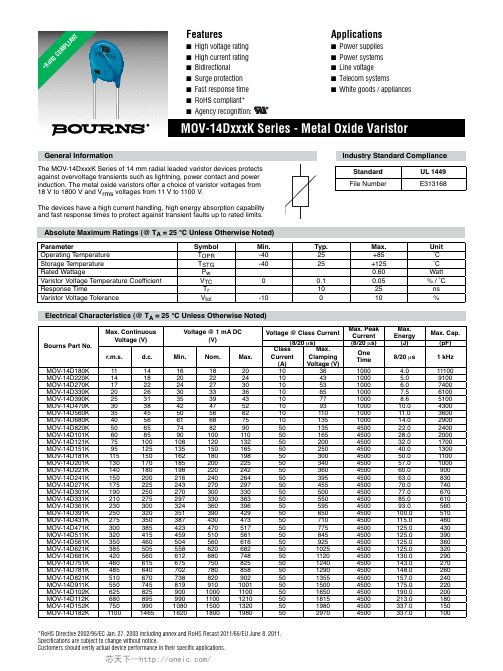
*RoHS Directive 2002/95/EC Jan. 27, 2003 including annex and RoHS Recast 2011/65/EU June 8, 2011. Specifi cations are subject to change without notice.Customers should verify actual device performance in their specifi c applications.Absolute Maximum Ratings (@ T A = 25 °C Unless Otherwise Noted)ParameterSymbol Min.Typ.Max.Unit Operating Temperature T OPR -4025+85˚C Storage Temperature T STG -4025+125˚C Rated WattageP w 0.60Watt Varistor Voltage Temperature Coeffi cient V TC 00.10.05 % / ˚C Response TimeT r 1025ns Varistor Voltage ToleranceV tol-1010%Electrical Characteristics (@ T A = 25 °C Unless Otherwise Noted)*Ro H S C O MP L I A N TBourns Part No.Max. Continuous Voltage (V)Voltage @ 1 mA DC(V)Voltage @ Class Current Max. PeakCurrent Max.Energy Max. Cap.(8/20 μs)(8/20 μs)(J)(pF)r.m.s.d.c.Min.Nom.Max.ClassCurrent(A)Max.Clamping Voltage (V)One Time 8/20 μs 1 kHz MOV-14D180K 111416182010361000 4.011100MOV-14D220K 141820222410431000 5.09100MOV-14D270K 172224273010531000 6.07400MOV-14D330K 2026303336106510007.56100MOV-14D390K 2531353943107710008.65100MOV-14D470K 30384247521093100010.04300MOV-14D560K 354550566210110100011.03600MOV-14D680K 405661687510135100014.02900MOV-14D820K 506574829050135450022.02400MOV-14D101K 60859010011050165450028.02000MOV-14D121K 7510010812013250200450032.01700MOV-14D151K 9512513515016550250450040.01300MOV-14D181K 11515016218019850300450050.01100MOV-14D201K 13017018520022550340450057.01000MOV-14D221K 14018019822024250360450060.0900MOV-14D241K 15020021624026450395450063.0830MOV-14D271K 17522524327029750455450070.0740MOV-14D301K 19025027030033050500450077.0670MOV-14D331K 21027529733036350550450085.0610MOV-14D361K 23030032436039650595450093.0560MOV-14D391K 250320351390429506504500100.0510MOV-14D431K 275350387430473507104500115.0460MOV-14D471K 300385423470517507754500125.0430MOV-14D511K 320415459510561508454500125.0390MOV-14D561K 350460504560616509254500125.0360MOV-14D621K 3855055586206825010254500125.0320MOV-14D681K 4205606126807485011204500130.0290MOV-14D751K 4606156757508255012404500143.0270MOV-14D781K 4856407027808585012904500148.0260MOV-14D821K 5106707388209025013554500157.0240MOV-14D911K 55074581991010015015004500175.0220MOV-14D102K 625825900100011005016504500190.0200MOV-14D112K 680895990110012105018154500213.0180MOV-14D152K 7509901080150013205019804500337.0150MOV-14D182K110014651620180019805029704500337.010014D 201K5Specifi cations are subject to change without notice.Customers should verify actual device performance in their specifi c applications.Product DimensionsDIMENSIONS:MM(INCHES)This is an RoHS compliant molded radial package with 100 % Sn plating on the terminations.Internal ConstructionHow to OrderMOV - 14D nn (n) K (TR)Model DesignatorMOV = Metal Oxide Varistor Disc Diameter 14D = 14 mmNominal Varistor VoltageSee Electrical Characteristics TableMultiplier of Voltage Digits 0 = No multiplier 1 = nn * 101 2 = nn * 102Varistor Voltage Tolerance K = 10 %PackagingBlank = BulkTR = Tape & Reel*Examples: MOV-14D270K = 27 V, Bulk PackMOV-14D331KTR = 330 V, T ape & Reel* Models MOV-14D911K, 102K, 112K, 152K and 182K are not available in Tape & Reel packaging.Part Number Dim. H (Max.)Dim. T (Max.)MOV-14D180K20.0(.787) 3.8(.150)MOV-14D220K 20.0(.787) 3.9(.154)MOV-14D270K 20.0(.787) 4.2(.165)MOV-14D330K 20.0(.787) 3.8(.150)MOV-14D390K20.0(.787) 4.0(.157)MOV-14D470K 20.0(.787) 4.2(.165)MOV-14D560K 20.0(.787) 4.3(.169)MOV-14D680K 20.0(.787) 4.4(.173)MOV-14D820K20.0(.787) 3.8(.150)MOV-14D101K 20.0(.787) 4.0(.157)MOV-14D121K20.0(.787) 4.2(.165)MOV-14D151K 20.0(.787) 4.4(.173)MOV-14D181K20.0(.787) 3.6(.142)MOV-14D201K 20.0(.787) 3.8(.150)MOV-14D221K 20.0(.787) 3.9(.154)MOV-14D241K 20.0(.787) 4.0(.157)MOV-14D271K 20.0(.787) 4.2(.165)MOV-14D301K20.0(.787) 4.4(.173)Part Number Dim. H (Max.)Dim. T (Max.)MOV-14D331K 20.0(.787) 4.6(.181)MOV-14D361K 20.0(.787) 4.8(.189)MOV-14D391K 20.0(.787) 5.0(.197)MOV-14D431K 20.0(.787) 5.2(.205)MOV-14D471K 20.0(.787) 5.4(.213)MOV-14D511K 20.0(.787) 5.5(.217)MOV-14D561K 22.0(.866) 6.0(.236)MOV-14D621K 22.0(.866) 6.4(.252)MOV-14D681K 22.0(.866) 6.5(.256)MOV-14D751K 22.0(.866) 6.7(.264)MOV-14D781K 22.0(.866) 6.9(.272)MOV-14D821K 22.0(.866)7.3(.287)MOV-14D911K*22.0(.866)7.7(.303)MOV-14D102K*22.0(.866)8.2(.323)MOV-14D112K*22.0(.866)8.7(.343)MOV-14D152K*22.0(.866)9.7(.382)MOV-14D182K*22.0(.866)11.7(.461)* Not available in Tape & Reel packaging.Specifi cations are subject to change without notice.Customers should verify actual device performance in their specifi c applications.1011001000101010101010Current (A)V o l t a g e (V )680560470390330270220180100100010000101010101010Current (A)V o l t a g e (V )18215211210291182178175168162156151147110010100010000101010101010Current (A)V o l t a g e (V )431391361331301271241221201181151121101820101010101010101010101010101010Performance Graphs V-I CharacteristicsMOV-14D180K to MOV-14D680KMOV-14D820K to MOV-14D431KMOV-14D471K to MOV-14D182KBournsPart Number Bourns Part Marking MOV-14D180K 14D180K MOV-14D220K 14D220K MOV-14D270K 14D270K MOV-14D330K 14D330K MOV-14D390K 14D390K MOV-14D470K 14D470K MOV-14D560K 14D560K MOV-14D680K 14D680K MOV-14D820K 14D820K MOV-14D101K 14D101K MOV-14D121K 14D121K MOV-14D151K 14D151K MOV-14D181K 14D181K MOV-14D201K 14D201K MOV-14D221K 14D221K MOV-14D241K 14D241K MOV-14D271K 14D271K MOV-14D301K 14D301K MOV-14D331K 14D331K MOV-14D361K 14D361K MOV-14D391K 14D391K MOV-14D431K 14D431K MOV-14D471K 14D471K MOV-14D511K 14D511K MOV-14D561K 14D561K MOV-14D621K 14D621K MOV-14D681K 14D681K MOV-14D751K 14D751K MOV-14D781K 14D781K MOV-14D821K 14D821K MOV-14D911K 14D821K MOV-14D102K 14D102K MOV-14D112K 14D112K MOV-14D152K 14D152K MOV-14D182K14D182KNOTE: The “5” marking on MOV products is for traceability of production assembly for quality assurance compliance.Typical Part MarkingPackaging InformationTAPE & REELItem Symbol14 mm Disc Reel Outside Diameter RD355(13.98) Reel Inner Diameter RD130(11.81) Tape Width RW55(2.165) Reel Width RW163(2.48) Pitch of Component P25.4 ± 1.0(1.00 ± 0.04) Feed Hole Pitch P012.7 ± 1.0(0.50 ± 0.04) Feed Hole Center to Pitch P18.95 ± 0.7(0.352 ± 0.3) Feed Hole Center to ComponentCenterP212.7 ± 1.0(0.50 ± 0.04)Lead to Lead Distance F7.50 ± 0.8(0.30 ± 0.03)Component AlignmentΔh4.0max.(0.157) max.Tape Width W18.0 ± 0.5(0.71 ± 0.02)Hole Down Tape Width W012.0 ± 0.8(0.47 ± 0.03)Hole Position W19.0 ± 0.5(0.35 ± 0.02)Hole Down Tape Position W23.0max.(0.12) max.Height From Center toComponent BaseH19.0 ± 1.0(0.75 ± 0.04)Seating Plane Height H016.0 ± 0.5(0.63 ± 0.02)Component Height H140.0max.(1.57) maxCrimp Length C2.60typ.(0.10) maxFeed Hole Diameter D04.0 ± 0.2(0.16 ± 0.08)Total Tape Thickness t0.6 ± 0.3(0.02 ± 0.01)Length of Clippped Height L1.0max.(0.04) maxQuantity per ReelMOV-14D180K – 14D391KMOV-14D431K - 14D182K-100050012/11Specifi cations are subject to change without notice.Customers should verify actual device performance in their specifi c applications.BULK60.0(2.36)Asia-Pacifi c:Tel: +886-2 2562-4117Fax: +886-2 2562-4116Europe:Tel: +41-41 768 5555Fax: +41-41 768 5510The Americas:Tel: +1-951 781-5500Fax: +1-951 781-5700NOTE: Models MOV-14D911K, 102K, 112K, 152K and 182K are not availablein Tape & Reel packaging.。
NZH3V0B,115;NZH10C,115;NZH8V2B,115;NZH7V5C,115;NZH6V2B,115;中文规格书,Datasheet资料
thermal resistance from junction to solder point
Min Typ Max Unit
[1] -
-
250 K/W
[2] -
-
125 K/W
[3] -
-
70 K/W
[1] Device mounted on an FR4 PCB, single-sided copper, tin-plated, mounting pad for cathode 1 cm2. [2] Device mounted on a ceramic PCB, Al2O3, standard footprint. [3] Soldering point of cathode tab.
Version SOD123F
Table 4. Marking codes
Type number
Marking code
NZH3V0B
CH
NZH3V3A
CJ
NZH3V6B
CK
NZH3V9B
CL
NZH4V3B
CM
NZH4V7B
CN
NZH5V1B
CP
NZH5V6B
CQ
NZH6V2B
CR
NZH6V8B
CS
5. Limiting values
Table 5. Limiting values In accordance with the Absolute Maximum Rating System (IEC 60134).
Symbol Parameter
Conditions
Min
Max Unit
IF Ptot
NZHxxx
NC7WZ240K8X, 规格书,Datasheet 资料
© 2005 Fairchild Semiconductor Corporation
DS500398
芯天下--/
NC7WZ240
Logic Symbol
IEEE/IEC
Connection Diagrams
Pin Assignments for US8
General Description
The NC7WZ240 is a Dual Inverting Buffer with independent active LOW enables for the 3-STATE outputs. The Ultra High Speed device is fabricated with advanced CMOS technology to achieve superior switching performance with high output drive while maintaining low static power dissipation over a broad VCC operating range. The device is specified to operate over the 1.65V to 5.5V VCC operating range. The inputs and outputs are high impedance when VCC is 0V. Inputs tolerate voltages up to 5.5V independent of VCC operating range. Outputs tolerate voltages above VCC when in the 3-STATE condition.
NC7WV125K8X, 规格书,Datasheet 资料
Pad Assignments for MicroPak
(Top Thru View)
2
芯天下--/
NC7WV125
Absolute Maximum Ratings(Note 1)
Supply Voltage (VCC) DC Input Voltage (VIN) DC Output Voltage (VOUT) HIGH or LOW State (Note 2) VCC = 0V DC Input Diode Current (IIK) VIN < 0V DC Output Diode Current (IOK) VOUT < 0V VOUT > VCC DC Output Source/Sink Current (IOH/IOL) DC VCC or Ground Current per Supply Pin (ICC or Ground) Storage Temperature Range (TSTG)
Note 1: Absolute Maximum Ratings: are those values beyond which the safety of the device cannot be guaranteed. The device should not be operated at these limits. The parametric values defined in the Electrical Characteristics tables are not guaranteed at the absolute maximum ratings. The “Recommended Operating Conditions” table will define the conditions for actual device operation. Note 2: IO Absolute Maximum Rating must be observed. Note 3: Unused inputs must be held HIGH or LOW. They may not float.
NC7SZ157P6X,NC7SZ157P6X,NC7SZ157P6X,NC7SZ157L6X,NC7SZ157FHX, 规格书,Datasheet 资料
®TinyLogic UHS 2-Input Non-Inverting MultiplexerFeaturesBroad V CC Operating Range: 1.65V to 5.5VUltra High-SpeedPower Down High-Impedance Inputs/OutputsOver-Voltage Tolerance Inputs Facilitate 5V to 3V TranslationProprietary Noise/EMI Reduction CircuitryUltra-Small MicroPak™ PackagesSpace-Saving SC70 Package DescriptionThe NC7SZ157 is a single, high performance, 2-to-1 CMOS non-inverting multiplexer from Fairchild’s Ultra-High Speed series of TinyLogic®. The device is fabricated with advanced CMOS technology to achieve ultra high speed with high output drive while maintaining low static power dissipation over a broad V CC operating range. The device is specified to operate over the 1.65V to 5.5V V CC operating range. The inputs and outputs are high impedance when V CC is 0V. Inputs tolerate voltages up to 5.5V independent of V CC operating range.Ordering InformationPart Number Top Mark EcoStatus Package PackingMethodNC7SZ157P6X ZF7 RoHS 6-Lead SC70, EIAJ SC-88, 1.25mm Wide 3000 Units on Tape & ReelNC7SZ157L6X B9 RoHS 6-Lead MicroPak™, 1.00mm Wide 5000 Units on Tape & ReelNC7SZ157FHX B9 Green 6-Lead, MicroPak2, 1x1mm Body, .35mm Pitch 5000 Units on Tape & ReelFor Fairchild’s definition of Eco Status, please visit: /company/green/rohs_green.html.NC7SZ157 — TinyLogic ® UHS 2-Input Non-Inverting MultiplexerFigure 1. Logic SymbolPin ConfigurationsFigure 2. SC70 (Top View)Figure 3. MicroPak™ (Top Through View)Figure 4. Pin 1 OrientationNotes:1. AAA represents product code top mark (see Ordering Information ).2. Orientation of top mark determines pin one location.3. Reading the top mark left to right, pin one is the lower left pin.Pin DefinitionsPin # SC70Pin # MicroPakNameDescription1 1 I 1 Data Input2 2 GND Ground3 3 I 0 Data Input4 4 Z Output5 5 V CC Supply Voltage6 6 S Control InputFunction TableNC7SZ157 — TinyLogic ® UHS 2-Input Non-Inverting MultiplexerSymbol Parameter Min. Max. UnitV CC Supply Voltage -0.5 7.0 V V IN DC Input Voltage -0.5 7.0 V V OUT DC Output Voltage -0.57.0 V I IK DC Input Diode Current V IN ≤ 0.5V -50 mA I OK DC Output Diode Current V OUT ≤ -0.5V-50 mA I OUT DC Output Current±50 mA I CC or I GND DC V CC or Ground Current±50 mA T STG Storage Temperature Range -65 +150 °C T J Junction Temperature Under Bias+150 °C T L Junction Lead Temperature (Soldering, 10 Seconds)+260°CP DPower Dissipation at +85°CSC70-6 180 mW MicroPak-6 130 MicroPak2-6 120ESD Human Body Model, JEDEC:JESD22-A114 4000 VCharge Device Model, JEDEC:JESD22-C1012000Recommended Operating ConditionsThe Recommended Operating Conditions table defines the conditions for actual device operation. Recommended operating conditions are specified to ensure optimal performance to the datasheet specifications. Fairchild does not recommend exceeding them or designing to Absolute Maximum Ratings.Symbol ParameterConditions Min. Max. UnitV CCSupply Voltage Operating1.655.50VSupply Voltage Data Retention1.50 5.50 V IN Input Voltage 0 5.5 V V OUT Output Voltage0 V CC V T A Operating Temperature-40+85 °Ct r , t f Input Rise and Fall TimesV CC at 1.8V ± 0.15V, 2.5V ± 0.2V0 20 ns/VV CC at 3.3V ± 0.3V 0 10 V at 5.0V ± 0.5V5® UHS 2-Input Non-Inverting MultiplexerV OHHIGH LevelOutput VoltageV IN =V IL or V IH I OH = -100µAV2.30 2.20 2.30 2.203.00 2.90 3.00 2.904.50 4.40 4.50 4.401.65V IN =V ILor V IHI OH = -4mA1.29 1.52 1.292.30 I OH = -8mA1.902.15 1.903.00 I OH = -16mA2.40 2.80 2.403.00 I OH = -24mA 2.30 3.68 2.304.50 I OH = -32mA 3.904.203.80V OLLOW LevelOutput Voltage1.65V IN =V IL or V IHI OL = 100µA 0 0.10 0.10V2.30 0 0.10 0.103.00 0 0.10 0.104.50 0 0.10 0.101.65V IN =V ILor V IHI OL = 4mA0.08 0.24 0.24 V2.30 I OL = 8mA0.10 0.30 0.30 3.00 I OL = 16mA0.15 0.40 0.40 3.00 I OL = 24mA 0.22 0.55 0.55 4.5 I OL = 32mA0.22 0.55 0.55 I IN Input Leakage Current0 to 5.50V IN =5.5V, GND±0.1±1µA I OFF Power OffLeakage Current0 V IN or V OUT =5.5V 1 10 µAI CCQuiescent SupplyCurrent1.65 to 5.50 V IN =5.5V, GND10µA® UHS 2-Input Non-Inverting Multiplexert PLH, t PHLFigure 5Figure 6Propagation Delay I n to ZC L =15pF, R L =1M Ω, 5.00 ± 0.50 1.2 3.5 5.8 1.2 6.1 3.30 ± 0.30 0.8 2.6 3.9 0.8 4.2 5.00 ± 0.500.5 1.9 3.1 0.5 3.3 Propagation Delay S to Z3.30 ± 0.30 C L =50pF, R L =500Ω, 1.2 3.24.8 1.25.2 5.00 ± 0.50 0.8 2.4 3.8 0.8 4.1 Propagation Delay I n to Z3.30 ± 0.30 C L =50pF, R L =500Ω,1.2 3.2 4.6 1.2 5.05.00 ± 0.50 0.8 2.4 3.7 0.8 4.0C IN Input Capacitance 0.002pFC PDPower DissipationCapacitance (4)3.3014pF Figure 75.00 17Note:4. C PD is defined as the value of the internal equivalent capacitance which is derived from dynamic operatingcurrent consumption (I CCD ) at no output loading and operating at 50% duty cycle. C PD is related to I CCD dynamic operating current by the expression: I CCD =(C PD )(V CC )(f IN )+(I CC static).Note:5. C L includes load and stray capacitance.Input PRR=1.0MHz, t w =500ns.Figure 5. AC Test CircuitFigure 6. AC WaveformsInput=AC Waveform; PRR=Variable; Duty Cycle=50%.® UHS 2-Input Non-Inverting MultiplexerDETAIL ASCALE: 60X1.000.801.100.800.10C0.250.100.460.260.20GAGE PLANE(R0.10)30°0°SEATING PLANEC0.100.00NOTES: UNLESS OTHERWISE SPECIFIEDA) THIS PACKAGE CONFORMS TO EIAJ SC-88, 1996.B) ALL DIMENSIONS ARE IN MILLIMETERS. C) DIMENSIONS DO NOT INCLUDE BURRS OR MOLD FLASH.D) DRAWING FILENAME: MKT-MAA06AREV62.10±0.300.10A B0.651.30(0.25)0.300.15131.300.40 MINSEE DETAIL ALAND PATTERN RECOMMENDATIONFigure 8. 6-Lead, SC70, EIAJ SC-88, 1.25mm WidePackage drawings are provided as a service to customers considering Fairchild components. Drawings may change in any manner without notice. Please note the revision and/or date on the drawing and contact a Fairchild Semiconductor representative to verify or obtain the most recent revision. Package specifications do not expand the terms of Fairchild’s worldwide terms and conditions, specifically the warranty therein, which covers Fairchild products.Always visit Fairchild Semiconductor’s online packaging area for the most recent package drawings: /packaging/.® UHS 2-Input Non-Inverting Multiplexer2. DIMENSIONS ARE IN MILLIMETERS1. CONFORMS TO JEDEC STANDARD M0-252 VARIATION UAAD MAC06AREVCNotes:3. DRAWING CONFORMS TO ASME Y14.5M-1994TOP VIEWRECOMMENED LAND PATTERNBOTTOM VIEWA0.55MAX0.05C(0.52)(0.30)6X 1X6X PIN 1DETAIL A0.075 X 45CHAMFER0.250.150.350.250.400.300.5(0.05) 1.0DETAIL APIN 1 TERMINAL0.400.300.450.350.100.000.10C B A 0.05CC0.05C0.050.005X 5X 6X(0.13)4X6XFigure 9. 6-Lead, MicroPak™, 1.0mm WidePackage drawings are provided as a service to customers considering Fairchild components. Drawings may change in any manner without notice. Please note the revision and/or date on the drawing and contact a Fairchild Semiconductor representative to verify or obtain the most recent revision. Package specifications do not expand the terms of Fairchild’s worldwide terms and conditions, specifically the warranty therein, which covers Fairchild products.Always visit Fairchild Semiconductor’s online packaging area for the most recent package drawings: /packaging/.®UHS 2-Input Non-Inverting Multiplexer DETAIL A5XFigure 10. 6-Lead, MicroPak2, 1x1mm Body, .35mm PitchPackage drawings are provided as a service to customers considering Fairchild components. Drawings may change in any mannerwithout notice. Please note the revision and/or date on the drawing and contact a Fairchild Semiconductor representative to verifyor obtain the most recent revision. Package specifications do not expand the terms of Fairchild’s worldwide terms and conditions, specificallythe warranty therein, which covers Fairchild products.Always visit Fairchild Semiconductor’s online packaging area for the most recent package drawings:/packaging/.NC7SZ157 — TinyLogic ® UHS 2-Input Non-Inverting Multiplexer。
蓝海微芯 LJD-eWINA8-LH080T(K) 产品规格书说明书
LJD-eWINA8-LH080T(K)产品规格书目录■1. Cortex-A8&Win CE6.0系列嵌入式触控一体机 (2)1.1基本安全注意事项 (2)1.2 修订历史 (2)■2. Cortex-A8&Win CE6.0系列产品规格 (3)2.1 产品规格 (3)2.2 接口设置和功能 (5)2.3 安装尺寸 (7)2.4 安装示意图 (10)LJD-eWINA8-LH080T安装示意图 (10)LJD-eWINA8-LH080H安装示意图: (10)2.5 Cortex-A8&Win CE6.0系列产品配件及可接外围设备说明 (12)■3. 产品保修及供货周期正常 (13)■4. 后记 (14)■1. Cortex-A8&Win CE6.0系列嵌入式触控一体机本手册包含了LJD-eWINA8-LH080T(K)型嵌入式触控一体机的硬件规格、使用和安装过程中的注意事项。
在使用LJD-eWINA8-LH080T(K)型人机界面之前请仔细阅读本手册1.1基本安全注意事项1.1.1 注意事项● 请确保所有电缆接头都牢固连接到LJD-eWINA8-LH080T(K)上。
●为了保证设备安全,请在接线之前拔下LJD-eWINA8-LH080T(K)的电源线。
● 请勿用力或用硬物按压LJD-eWINA8-LH080T(K) 的显示屏,以免造成触摸屏和液晶屏的损坏。
● 需要返修的产品,客户需将返修产品包装好避免运输过程中显示屏、触摸屏的碎裂以及产品外壳的损坏。
一切后果由客户承担。
1.1.2 警告(1)系统设计● 请勿在LJD-eWINA8-LH080T(K)上制作可能危及设备及人员安全的开关,如紧急停机开关,这些操作应该由独立的硬件开关来执行,以防止电缆以及其它相关设备的损坏导致可能造成重大事故。
● 请勿将LJD-eWINA8-LH080T(K)用作可能造成严重人身伤害、设备损坏或系统停机等重要报警的警示设备。
N32L40xx8 xB数据手册说明书
N32L40xx8/xB数据手册N32L40x系列采用32-bit ARM Cortex-M4F内核,最高工作主频64MHz,支持浮点运算和DSP指令,集成高达128KB嵌入式加密Flash,24KB SRAM,集成丰富的高性能模拟器件,内置1个12bit 4.5Msps ADC,2个独立轨到轨运算放大器,2个高速比较器,1个12bit 1Msps DAC,集成多达320段的Segment LCD驱动,集成多路U(S)ART、I2C、SPI、USB、CAN等数字通信接口,内置密码算法硬件加速引擎。
关键特性●内核CPU―32位ARM Cortex-M4内核+FPU,单周期硬件乘除法指令,支持DSP指令和MPU―内置2KB指令Cache缓存,支持Flash加速单元执行程序0等待―最高主频64MHz,80DMIPS●加密存储器―高达128KByte片内Flash,支持加密存储、多用户分区管理及数据保护、硬件ECC检查,10万次擦写次数,10年数据保持―24KByte SRAM,包括16Kbyte SRAM1(在STOP2模式下可配置为保持)和8Kbyte SRAM2(在STANDBY和STOP2模式下可配置为保持),支持硬件奇偶校验●低功耗管理―STANDBY模式:1.5uA,所有备份寄存器保持,IO保持,可选RTC Run,8KByte SRAM2保持,快速唤醒―STOP2模式:3uA、RTC Run、8KByte SRAM2保持、CPU寄存器保持、IO保持、快速唤醒―RUN模式:60uA/MHz@64MHz―LPRUN模式:PLL关闭,MSI作为系统主时钟,MR关闭,LPR开启,USB/CAN/SAC电源关闭,其他外设可选●Segment LCD显示驱动,最高支持176段(4x44)或320段(8x40)●高性能模拟接口―1个12bit 4.5Msps ADC,多精度可配置,6位模式下采样率高达8Msps,最多16个外部单端输入通道,支持差分模式―2个轨到轨运算放大器,内置最大32倍可编程增益放大器―2个高速模拟比较器,内置64级可调比较基准,COMP1支持在STOP2模式下工作―1个12bit DAC,采样率1Msps―内部2.048V独立参考电压参考源―内部集成低压检测单元●时钟―HSE:4MHz~32MHz外部高速晶体―LSE:32.768KHz外部低速晶体―HSI:内部高速RC16MHz―MSI:内部多速RC100K ~ 4MHz―LSI:内部低速RC 40KHz―内置高速PLL―MCO:支持1路时钟输出,可配置为低速或高速时钟输出●复位―支持上电/欠压/外部引脚复位―支持看门狗复位●最大支持64个GPIOs●通信接口―5个U(S)ART接口,其中3个USART接口(支持ISO7816,IrDA,LIN),2个UART接口―1个LPUART,支持STOP2模式唤醒MCU―2个SPI接口,速度高达16Mbps,支持I2S通信―2个I2C接口,速率高达1MHz,主从模式可配,从机模式下支持双地址响应―1个USB 2.0全速设备接口―1个CAN 2.0A/B总线接口●1个DMA控制器,支持8通道,通道源地址及目的地址任意可配●1个RTC实时时钟,支持闰年万年历,闹钟事件,周期性唤醒,支持内外部时钟校准●定时计数器―2个16bit高级定时计数器,支持输入捕获,互补输出,正交编码输入,最高控制精度9.25ns;每个定时器有4个独立的通道,其中3个通道支持6路互补PWM输出―5个16bit通用定时计数器,每个定时器有4个独立通道,支持输入捕获/输出比较/PWM输出―2个16bit基础定时计数器―1个16bit低功耗定时计数器,支持双脉冲计数功能,可在STOP2模式下工作―1个24bit SysTick―1个7bit窗口看门狗(WWDG)―1个12bit独立看门狗(IWDG)●编程方式―支持SWD/JTAG在线调试接口―支持UART和USB Bootloader●安全特性―内置密码算法硬件加速引擎―支持AES、DES、TDES、SHA1/224/256、SM1、SM3、SM4和SM7算法―闪存存储加密、多用户分区管理单元(MMU)―TRNG真随机数发生器―CRC16/32运算―支持写保护(WRP),多种读保护(RDP)等级(L0/L1/L2)―支持安全启动,程序加密下载,安全更新―支持外部时钟失效检测,入侵检测●96位UID和128位UCID●工作条件―工作电压范围:1.8V~3.6V―工作温度范围:-40℃~105℃―ESD:±4KV(HBM模型),±1KV(CDM模型)●封装―QFN32(4mm×4mm)―QFN48(6mm×6mm)―LQFP48(7mm×7mm)―QFN64(8mm×8mm)―LQFP64(10mm×10mm)―LQFP80(12mm×12mm)●订购型号目录1 产品简介 (11)命名规则 (12)器件一览 (13)2 功能简介 (14)处理器内核 (14)存储器 (14)嵌入式闪存存储器(FLASH) (14)嵌入式SRAM (15)嵌套的向量式中断控制器(NVIC) (15)外部中断/事件控制器(EXTI) (15)时钟系统 (15)启动模式 (16)供电方案 (16)复位 (17)可编程电压监测器 (17)电压调压器 (17)低功耗模式 (17)直接存储器存取(DMA) (18)实时时钟(RTC) (18)定时器和看门狗 (18)低功耗定时器(LPTIM) (18)基本定时器(TIM6和TIM7) (19)通用定时器(TIMx) (19)高级控制定时器(TIM1和TIM8) (20)系统时基定时器(Systick) (20)看门狗定时器(WDG) (20)I2C总线接口 (21)通用同步/异步收发器(USART) (22)低功耗通用异步接收器(LPUART) (24)串行外设接口(SPI) (24)串行音频接口(I2S) (25)控制器局域网络(CAN) (26)通用串行总线(USB) (26)通用输入输出接口(GPIO) (27)段式液晶显示驱动(LCD) (28)模拟/数字转换器(ADC) (28)运算放大器(OPAMP) (29)模拟比较器(COMP) (29)数字/模拟转换(DAC) (30)温度传感器(TS) (30)循环冗余校验计算单元(CRC) (30)密码算法硬件加速引擎(SAC) (31)唯一设备序列号(UID) (31)串行单线JTAG调试口(SWJ-DP) (31)3 引脚定义和描述 (32)封装示意图 (32)QFN32 (32)QFN48 (33)LQFP48 (34)QFN64 (35)LQFP64 (36)LQFP80 (37)引脚定义 (38)4 电气特性 (45)测试条件 (45)最小和最大数值 (45)典型数值 (45)典型曲线 (45)负载电容 (45)引脚输入电压 (45)供电方案 (46)电流消耗测量 (47)绝对最大额定值 (47)工作条件 (48)通用工作条件 (48)上电和掉电时的工作条件 (48)内嵌复位和电源控制模块特性 (48)内置参考电压 (49)供电电流特性 (49)外部时钟源特性 (51)内部时钟源特性 (54)从低功耗模式唤醒的时间 (56)PLL特性 (56)FLASH存储器特性 (57)绝对最大值(电气敏感性) (58)I/O端口特性 (58)NRST引脚特性 (61)TIM定时器和看门狗特性 (62)I2C接口特性 (64)SPI/I2S接口特性 (65)USB接口特性 (69)控制器局域网络(CAN)接口特性 (70)12位模数转换器(ADC)电气参数 (70)内部参考源(VREFBUFF)电气参数 (74)12位DAC电气参数 (74)运算放大器(OPAMP)电气参数 (75)比较器2(COMP2)电气参数 (76)比较器1(COMP1)电气参数 (77)液晶显示驱动器(Segment LCD)特性 (77)温度传感器(TS)特性 (78)5 封装尺寸 (79)QFN32 (79)QFN48 (80)LQFP48 (81)QFN64 (82)LQFP64 (83)LQFP80 (84)丝印说明 (85)6 版本历史 (86)7 声明 (89)表目录表1-1N32L40X系列资源配置 (13)表2-1定时器功能比较 (18)表3-1引脚定义 (38)表4-1电压特性 (47)表4-2电流特性 (47)表4-3温度特性 (47)表4-4通用工作条件 (48)表4-5上电和掉电时的工作条件 (48)表4-6内嵌复位和电源控制模块特性 (48)表4-7内置参考电压 (49)表4-8运行模式下的典型电流消耗,数据处理代码从内部闪存中运行 (49)表4-9睡眠模式下的典型电流消耗 (50)表4-10运行模式下的典型电流消耗,数据处理代码从内部闪存中运行 (50)表4-11睡眠模式下的典型电流消耗 (50)表4-12停机和待机模式下的典型电流消耗 (51)表4-13高速外部用户时钟特性(B YPASS模式) (51)表4-14低速外部用户时钟特性(B YPASS模式) (52)表4-15HSE4~32MH Z振荡器特性(1)(2) (53)表4-16LSE振荡器特性(F LSE=32.768K H Z)(1)(2)(4)(5) (54)表4-17MSI振荡器特性(1) (55)表4-18HSI振荡器特性(1)(2) (55)表4-19LSI振荡器特性(1) (56)表4-20低功耗模式的唤醒时间 (56)表4-21PLL特性 (56)表4-22闪存存储器特性 (57)表4-23闪存存储器寿命和数据保存期限 (58)表4-24ESD绝对最大值 (58)表4-25电气敏感性 (58)表4-26I/O静态特性 (58)表4-27IO输出驱动能力特性 (60)表4-28输出电压特性 (60)表4-29输入输出交流特性(1) (60)表4-30NRST引脚特性 (61)表4-31TIM1/8特性 (62)表4-32TIM2/3/4/5/6/7/9特性 (63)表4-33LPTIMER特性 (63)表4-34IWDG最大和最小计数复位时间(LSI=40K H Z) (63)表4-35WWDG最大和最小计数复位时间(APB1PCLK1=16MH Z) (63)表4-36I2C接口特性 (64)表4-37SPI特性(1) (65)表4-38I2S特性(1) (67)表4-39USB启动时间 (69)表4-40USB直流特性 (70)表4-41全速USB电气特性 (70)表4-42ADC特性 (70)表4-43ADC采样时间(1) (71)表4-44ADC精度–局限的测试条件(1)(2) (72)表4-45V REFBUFF特性 (74)表4-46DAC特性(1) (74)表4-47OPAMP特性 (75)表4-48COMP2特性 (76)表4-49COMP1特性 (77)表4-50COMP1低功耗模式特性 (77)表4-51LCD控制器特性 (77)表4-52温度传感器特性 (78)图目录图1-1N32L40X系列框图 (11)图1-2N32L40X系列订货代码信息图示 (12)图2-1存储器映射图 (14)图2-2时钟树 (16)图3-1N32L403系列QFN32引脚分布 (32)图3-2N32L406系列QFN48引脚分布 (33)图3-3N32L406系列LQFP48引脚分布 (34)图3-4N32L406系列QFN64引脚分布 (35)图3-5N32L406系列LQFP64引脚分布 (36)图3-6N32L406系列LQFP80引脚分布 (37)图4-1引脚的负载条件 (45)图4-2引脚输入电压 (46)图4-3供电方案 (46)图4-4电流消耗测量方案 (47)图4-5外部高速时钟源的交流时序图 (52)图4-6外部低速时钟源的交流时序图 (53)图4-7使用8MH Z晶体的典型应用 (53)图4-8使用32.768KH Z晶体的典型应用 (54)图4-9输入输出交流特性定义 (61)图4-10建议的NRST引脚保护 (62)图4-11I2C总线交流波形和测量电路(1) (65)图4-12SPI时序图–从模式和CLKPHA=0 (66)图4-13SPI时序图–从模式和CLKPHA=1(1) (67)图4-14SPI时序图–主模式(1) (67)图4-15I2S从模式时序图(飞利浦协议)(1) (69)图4-16I2S主模式时序图(飞利浦协议)(1) (69)图4-17USB时序:定义数据信号的上升和下降时间 (70)图4-18ADC精度特性 (73)图4-19使用ADC典型的连接图 (73)图4-20供电电源和参考电源去藕线路(V REF+与V DDA相连) (74)图5-1QFN32封装尺寸 (79)图5-2QFN48封装尺寸 (80)图5-3LQFP48封装尺寸 (81)图5-4QFN64封装尺寸 (82)图5-6LQFP80封装尺寸 (84)图5-7丝印说明 (85)1产品简介N32L40x系列微控制器产品采用高性能32位ARM Cortex™-M4F内核,集成浮点运算单元(FPU)和数字信号处理(DSP),支持并行计算指令。
ZXMN6A08KTC;中文规格书,Datasheet资料
A Product Line ofDiodes IncorporatedZXMN6A08K60V N-CHANNEL ENHANCEMENT MODE MOSFET Product SummaryV(BR)DSS R DS(on)I DT A = 25°C60V80mΩ @ V GS= 10V 7.90A150mΩ @ V GS= 4.5V 5.75ADescription and ApplicationsThis new generation MOSFET has been designed to minimize the on-state resistance (R DS(on)) and yet maintain superior switchingperformance, making it ideal for high efficiency power managementapplications.•Backlighting•DC-DC Converters•Power management functionsFeatures and Benefits•Low on-resistance•Fast switching speed•“Green” component and RoHS compliant (Note 1)Mechanical Data• Case:TO-252•Case Material: Molded Plastic, “Green” Molding Compound. ULFlammability Classification Rating 94V-0 (Note 1)•Moisture Sensitivity: Level 1 per J-STD-020D•Terminals Connections: See Diagram•Terminals: Matte Tin Finish annealed over Copper leadframe.Solderable per MIL-STD-202, Method 208•Weight: 0.33 grams (approximate)Ordering Information(Note 1)Product Marking Reel size (inches) Tape width (mm)Quantity per reel ZXMN6A08KTC SeeBelow 13 162,500 Note: 1. Diodes, Inc. defines “Green” products as those which are Eu RoHS compliant and contain no halogens or antimony compounds; further information about Diodes Inc.’s “Green” Policy can be found on our website. For packaging details, go to our website.Marking InformationTOP VIEW PIN OUT -TOP VIEWGEquivalent CircuitG SDDZXMN = Product Type Marking Code, Line 16A08 = Product Type Marking Code, Line 2YYWW = Date Code MarkingYY = Year (ex: 09 = 2009)WW = Week (01-52)YYWWZXMN6A08Please click here to visit our online spice models database.Maximum Ratings@T A = 25°C unless otherwise specifiedCharacteristic SymbolValueUnit Drain-Source voltage V DSS60 VGate-Source voltage V GS±20 VContinuous Drain current V GS = 10V (Note 3)I D7.90A T A=70°C (Note 3) 6.30(Note 2) 5.36Pulsed Drain current V GS= 10V (Note 4) I DM24.3 A Continuous Source current (Body diode) (Note 3) I S9.0 A Pulsed Source current (Body diode) (Note 4) I SM24.3 AThermal Characteristics@T A = 25°C unless otherwise specifiedCharacteristic SymbolValueUnitPower dissipation Linear derating factor (Note 2)P D4.1333.0WmW/°C (Note 3)8.9471.5(Note 5)2.1216.9Thermal Resistance, Junction to Ambient (Note 2)RθJA30.3°C/W (Note 3) 14.0(Note 5) 59.1Thermal Resistance, Junction to Lead (Note 6) RθJL 2.77Operating and storage temperature range T J, T STG-55 to 150 °CNotes: 2. For a device surface mounted on 50mm x 50mm x 1.6mm FR4 PCB with high coverage of single sided 2oz copper, in still air conditions; the device is measured when operating in a steady-state condition.3. Same as note 2, except the device is measured at t ≤ 10 sec.4. Same as note 2, except the device is pulsed with D = 0.02 and pulse width 300 µs. The pulse current is limited by the maximum junction temperature.5. For a device surface mounted on 25mm x 25mm x 1.6mm FR4 PCB with high coverage of single sided 1oz copper, in still air conditions; the device ismeasured when operating in a steady-state condition.6. Thermal resistance from junction to solder-point (at the end of the drain lead).Thermal Characteristics0.00.51.01.52.02.53.03.54.04.5Derating CurveTemperature (°C)M a x P o w e r D i s s i p a t i o n (W )Transient Thermal ImpedanceT h Pulse Width (s)Pulse Power DissipationPulse Width (s) M a x P o w e r D i s s i p a t i o n (W )Transient Thermal ImpedancePulse Width (s) TElectrical Characteristics @T A = 25°C unless otherwise specifiedCharacteristic Symbol Min Typ Max Unit Test ConditionOFF CHARACTERISTICS Drain-Source Breakdown Voltage BV DSS 60 ⎯ ⎯ V I D = 250μA, V GS = 0V Zero Gate Voltage Drain Current I DSS ⎯ ⎯ 0.5 μA V DS = 60V, V GS = 0V Gate-Source Leakage I GSS ⎯ ⎯ ±100nAV GS = ±20V, V DS = 0VON CHARACTERISTICS Gate Threshold VoltageV GS(th) 1.0 ⎯ 3.0 V I D = 250μA, V DS = V GS Static Drain-Source On-Resistance (Note 7) R DS (ON) ⎯ ⎯ 0.080 Ω V GS = 10V, I D = 4.8A 0.150 V GS = 4.5V, I D = 4.2A Forward Transconductance (Notes 7 & 8) g fs ⎯ 6.6 ⎯ S V DS = 15V, I D = 4.8ADiode Forward Voltage (Note 7) V SD ⎯ 0.88 0.95 V I S = 4.0A, V GS = 0VReverse recovery time (Note 8) t rr 19.2 ⎯ ns I S = 1.4A, di/dt= 100A/μsReverse recovery charge (Note 8) Q rr ⎯ 30.3 ⎯ nC DYNAMIC CHARACTERISTICS (Note 8) Input Capacitance C iss ⎯ 459 ⎯ pF V DS = 40V, V GS = 0Vf= 1MHz Output CapacitanceC oss ⎯ 44.2 ⎯ pF Reverse Transfer Capacitance C rss ⎯ 24.1 ⎯ pF Total Gate Charge Q g ⎯ 3.8 ⎯ nC V GS = 4.5VV DS = 30V I D = 1.4ATotal Gate Charge Q g ⎯ 5.8 ⎯ nC V GS = 10VGate-Source Charge Q gs ⎯ 1.4 ⎯ nC Gate-Drain ChargeQ gd ⎯ 1.9 ⎯ nC Turn-On Delay Time (Note 9) t D(on) ⎯ 2.6 ⎯ ns V DD = 30V, V GS = 10VI D = 1.5A, R G ≅ 6.0Ω Turn-On Rise Time (Note 9) t r ⎯ 2.1 ⎯ ns Turn-Off Delay Time (Note 9) t D(off) ⎯ 12.3 ⎯ ns Turn-Off Fall Time (Note 9)t f⎯4.6⎯nsNotes:7. Measured under pulsed conditions. Pulse width ≤ 300μs; duty cycle ≤ 2% 8. For design aid only, not subject to production testing.9. Switching characteristics are independent of operating junction temperatures.Typical Characteristics0.11100.11100.1110Output CharacteristicsI D D r a i n C u r r e n t (A )V DS Drain-Source Voltage (V)Output CharacteristicsI D D r a i n C u r r e n t (A )V DS Drain-Source Voltage (V)I D D r a i n C u r r e n t (A )Normalised Curves v TemperatureN o r m a l i s e d R D S (o n ) a n d V G S (t h )Tj Junction Temperature (°C)On-Resistance v Drain CurrentR D S (o n ) D r a i n -S o u r c e O n -R e s i s t a n c e (Ω)I D Drain Current (A)Typical Characteristics - continuedV DS - Drain - Source Voltage (V)Gate-Source Voltage v Gate ChargeCapacitance v Drain-Source VoltageQ - Charge (nC)V G S G a t e -S o u r c e V o l t a g e (V )Test CircuitsCurrent Gate charge test circuitSwitching time test circuitBasic gate charge waveform Switching time waveformsV DS GV GS90%10%DDV DSDPackage Outline DimensionsDIM Inches Millimeters DIM Inches Millimeters Min Max Min Max Min Max Min MaxA 0.086 0.094 2.18 2.39 e 0.090 BSC 2.29 BSCA1 - 0.005 - 0.127 H 0.370 0.410 9.40 10.41b 0.020 0.035 0.508 0.89 L 0.055 0.070 1.40 1.78b2 0.030 0.045 0.762 1.14 L1 0.108 REF 2.74 REFb3 0.205 0.215 5.21 5.46 L2 0.020 BSC 0.508 BSCc 0.018 0.024 0.457 0.61 L3 0.035 0.065 0.89 1.65c2 0.018 0.023 0.457 0.584 L4 0.025 0.040 0.635 1.016D 0.213 0.245 5.41 6.22 L5 0.045 0.060 1.14 1.52D1 0.205 - 5.21 - θ1° 0° 10° 0° 10°E 0.250 0.265 6.35 6.73 θ° 0° 15° 0° 15°- 4.32 - - - - - - E1 0.170Suggested Pad Layout6.20.244mm inches分销商库存信息: DIODESZXMN6A08KTC。
- 1、下载文档前请自行甄别文档内容的完整性,平台不提供额外的编辑、内容补充、找答案等附加服务。
- 2、"仅部分预览"的文档,不可在线预览部分如存在完整性等问题,可反馈申请退款(可完整预览的文档不适用该条件!)。
- 3、如文档侵犯您的权益,请联系客服反馈,我们会尽快为您处理(人工客服工作时间:9:00-18:30)。
®FeaturesUltra-High Speed: t PD 2.4ns (Typical) into 50pF at 5V V CCHigh Output Drive: ±24mA at 3V V CCBroad V CC Operating Range: 1.65V to 5.5VPower-Down, High-Impedance Inputs / Outputs Over-Voltage Tolerance Inputs Facilitate 5V to 3V TranslationProprietary Noise / EMI Reduction CircuitrySpace-Saving MicroPak™ and US8 Surface Mount Packages DescriptionThe NC7NZ04 is a triple inverter from Fairchild’s Ultra-High Speed (UHS) series of TinyLogic®. The device is fabricated with advanced CMOS technology to achieve ultra-high speed with high output drive while maintaining low static power dissipation over a broad V CC operating range. The device is specified to operate over the 1.65V to 5.5V V CC operating range. The inputs and output are high impedance when V CC is 0V. Inputs tolerate voltages up to 7V, independent of V CC operating voltage.IEEC/IECFigure 1. Logic SymbolFigure 2. Connection DiagramOrdering InformationPart Number Top Mark Package Packing MethodNC7NZ04K8X NZ04 8-Lead US8, JEDEC MO-187, Variation CA 3.1mm Wide 3000 Units on Tape & Reel 5000 Units on Tape & ReelNC7NZ04 — TinyLogic®UHS InverterFigure 3. US8Notes:1. AAA represents product code top mark (see ordering table).2. Orientation of top mark determines pin one location. Reading the top product code mark left to right, pin one isthe lower left pin.Figure 4. MicroPak™ (Top Through View)Pin DefinitionsPin # US8 Pin # MicroPak™ Name Description1 7 1AInputOutput2 6 3Y3 5 2AInputGround4 4 GNDOutput5 3 2YInput6 2 3AOutput7 1 1YVoltage8 8 V CC SupplyNC7NZ04 — TinyLogic ® UHS InverterSymbol Parameter Min. Max. UnitV CC Supply Voltage -0.5 7.0 V V IN DC Input Voltage -0.5 7.0 V V OUT DC Output Voltage -0.57.0 V I IK DC Input Diode Current V IN < -0.5V -50 mAV IN > 6.0V +20 I OK DC Output Diode Current V OUT < -0.5V-50mAV OUT > 6V, V CC =GND+20 I OUT DC Output Current±50 mA I CC or I GND DC V CC or Ground Current±50 mA T STG Storage Temperature Range -65 +150 °C T J Junction Temperature Under Bias+150 °C T L Junction Lead Temperature (Soldering, 10 Seconds)+260 °C P D Power Dissipation at +85°C250 mW ESD Human Body Model, JEDEC:JESD22-A114 4000 VCharge Device Model, JEDEC:JESD22-C1012000Recommended Operating ConditionsThe Recommended Operating Conditions table defines the conditions for actual device operation. Recommended operating conditions are specified to ensure optimal performance to the datasheet specifications. Fairchild does not recommend exceeding them or designing to Absolute Maximum Ratings.Symbol ParameterConditions Min. Max. UnitV CCSupply Voltage Operating 1.65 5.50 V Supply Voltage Data Retention1.5 5.5 V IN Input Voltage 0 5.5VV OUT Output Voltage0 V CC V T A Operating Temperature-40 +85 °C t r , t fInput Rise and Fall TimesV CC at 1.8V, 2.5V ± 0.2V 0 20 ns/VV CC at 3.3V ± 0.3V 0 10® UHS InverterV OHHIGH LevelOutput Voltage1.65V IN =V IL , I OH =-100µA1.55 1.651.55V 2.30 2.20 2.30 2.203.00 2.90 3.00 2.904.50 4.40 4.50 4.401.65 I OH =-4mA 1.29 1.52 1.292.30 I OH =-8mA 1.90 2.15 1.903.00 I OH =-16mA 2.40 2.80 2.40 3.00 I OH =-24mA 2.30 2.68 2.304.50 I OH =-32mA 3.80 4.20 3.80 V OLLOW LevelOutput Voltage1.65V IN =V IH , I OL =100µA0.00 0.10 0.10V2.30 0.00 0.10 0.103.00 0.00 0.10 0.104.50 0.00 0.10 0.101.65 I OL =4mA 0.80 0.24 0.242.30 I OL =8mA 0.10 0.30 0.303.00 I OL =16mA 0.15 0.40 0.40 3.00 I OL =24mA 0.22 0.55 0.554.50 I OL =32mA 0.22 0.55 0.55I IN Input LeakageCurrent0 to 5.50 ≤ V IN ≤ 5.5V±1 ±1 µAI OFF Power-OffLeakage Current0 V IN or V OUT =5.5V 1 10 µAI CCQuiescent SupplyCurrent1.65 to 5.50 V IN =5.5V, GND110µA® UHS Inverter3.30 ± 0.30 C L =50pF, R L =500Ω1.22.9 4.5 1.2 5.05.00 ± 0.50 0.8 2.43.60.8 4.0 C IN Input Capacitance 02.5pFC PDPower DissipationCapacitance (4)3.309pF Figure 75.00 11Note:4. C PD is defined as the value of the internal equivalent capacitance which is derived from dynamic operatingcurrent consumption (I CCD ) at no output lading and operating at 50% duty cycle. C PD is related to I CCD dynamic operating current by the expression: I CCD =(C PD )(V CC )(f IN )+(I CC static).Dynamic Switching CharacteristicsSymbol ParameterConditions V CCT A =25°c UnitTyp.V OLP Quiet Output Dynamic Peak V OLC L =50pF, V IH =5.0V, V IL =0V5.0 0.8 VV OLV Quiet Output Dynamic Valley V OL 5.0 -0.8 VNote:5. C L includes load and stray capacitance; inputsPRR=1.0MHz, t W =500ns.Figure 5. AC Test CircuitFigure 6. AC WaveformsInput=AC Waveform; t r =t f =1.8ns; PRR=10MHz; Duty Cycle =50%.Figure 7. I CCD Test Circuit® UHS InverterSIDE VIEWTOP VIEWRECOMMENDED LAND PATTERN0.50SEATING PLANE0.10-0.180.13A BC0.50DETAIL A0.4 TYPALL LEAD TIPS0.2C B A PIN 1 IDENTALL LEAD TIPS0.1C14DETAIL AGAGE PLANE0.12C. DIMENSIONS ARE EXCLUSIVE OF BURRS,D. DIMENSIONS AND TOLERANCES PERMOLD FLASH, AND TIE BAR EXTRUSIONS. B. DIMENSIONS ARE IN MILLIMETERS.A. CONFORMS TO JEDEC REGISTRATION MO-187 ANSI Y14.5M, 1994.0.90 MAX0.100.000.800.600.17-0.27(8X)0.30 (8X)0.20-0.350°-8°CSEATING PLANEE. FILE DRAWING NAME : MKT-MAB08Arev4Figure 8. 8-Lead US8, JEDEC MO-187, Variation CA, 3.1mm WidePackage drawings are provided as a service to customers considering Fairchild components. Drawings may change in any manner without notice. Please note the revision and/or date on the drawing and contact a Fairchild Semiconductor representative to verify or obtain the most recent revision. Package specifications do not expand the terms of Fairchild’s worldwide terms and conditions, specifically the warranty therein, which covers Fairchild products.Always visit Fairchild Semiconductor’s online packaging area for the most recent package drawings: /packaging/.Tape and Reel Specification® UHS Inverter(0.09)(0.1)(0.2)0.050.002XC0.05C43. DRAWING CONFORMS TO ASME Y.14M-19942. DIMENSIONS ARE IN MILLIMETERS1. PACKAGE CONFORMS TO JEDEC MO-255 VARIATION UAAD BOTTOM VIEW4. PIN 1 FLAG, END OF PACKAGE OFFSET MAC08AREV41235678Notes:8X0.250.35 3X 8X 1.040.58X 0.250.15 0.10C A B 0.05CTOP VIEWINDEX AREARecommended Landpattern0.10C0.55 MAX0.05CDETAIL A 0.350.25(0.15)(0.20)0.350.25DETAIL APIN #1 TERMINAL SCALE: 2X5. DRAWING FILE NAME: MKT-MAC08AREV4Figure 9. 8-Lead, MicroPak™, 1.0mm WidePackage drawings are provided as a service to customers considering Fairchild components. Drawings may change in any manner without notice. Please note the revision and/or date on the drawing and contact a Fairchild Semiconductor representative to verify or obtain the most recent revision. Package specifications do not expand the terms of Fairchild’s worldwide terms and conditions, specifically the warranty therein, which covers Fairchild products.Always visit Fairchild Semiconductor’s online packaging area for the most recent package drawings: /packaging/.NC7NZ04 — TinyLogic Array Array®UHS Inverter。