LM7805中文资料
7805稳压器的电路图和引脚介绍2
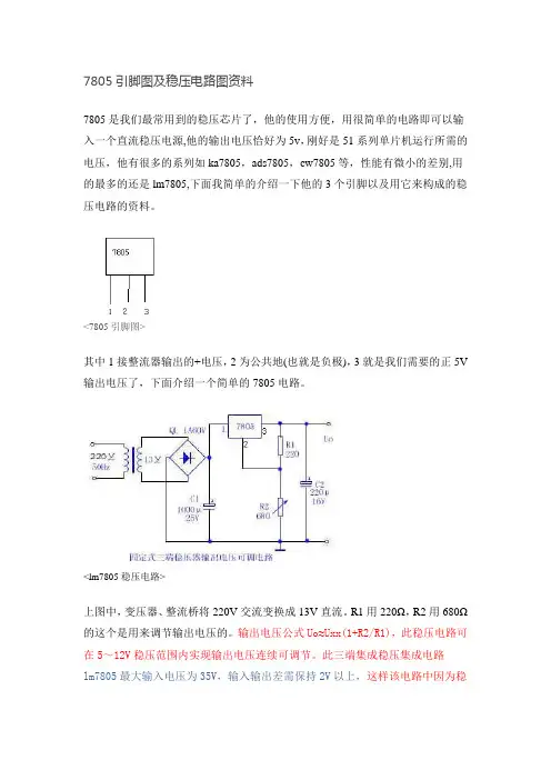
7805引脚图及稳压电路图资料
7805是我们最常用到的稳压芯片了,他的使用方便,用很简单的电路即可以输入一个直流稳压电源,他的输出电压恰好为5v,刚好是51系列单片机运行所需的电压,他有很多的系列如ka7805,ads7805,cw7805等,性能有微小的差别,用的最多的还是lm7805,下面我简单的介绍一下他的3个引脚以及用它来构成的稳压电路的资料。
<7805引脚图>
其中1接整流器输出的+电压,2为公共地(也就是负极),3就是我们需要的正5V 输出电压了,下面介绍一个简单的7805电路。
<lm7805稳压电路>
上图中,变压器、整流桥将220V交流变换成13V直流。
R1用220Ω,R2用680Ω的这个是用来调节输出电压的。
输出电压公式Uo≈Uxx(1+R2/R1),此稳压电路可在5~12V稳压范围内实现输出电压连续可调节。
此三端集成稳压集成电路
lm7805最大输入电压为35V,输入输出差需保持2V以上,这样该电路中因为稳
压器的直流输入电压是正14V,故该稳压电路的最大输出电压为正12V。
此电路的精度一般可达到0.04以上,用lm7805就能满足一般需求了。
7805手册
LM78XX/LM78XXA 3-Terminal 1A Positive Voltage Regulator May 2006The LM78XX series of three terminal positive regulators are available in the TO-220 package and with severalfixed output voltages, making them useful in a wide range of applications. Each type employs internal current limiting, thermal shut down and safe operating area pro-tection, making it essentially indestructible. If adequate heat sinking is provided, they can deliver over 1A output current. Although designed primarily as fixed voltageLM78XX/LM78XXA 3-Terminal 1A Positive Voltage RegulatorLM78XX/LM78XXA 3-Terminal 1A Positive Voltage RegulatorElectrical Characteristics (LM7805)Refer to the test circuits. -40°C < T J < 125°C, I O = 500mA, V I = 10V , C I = 0.1 µ F , unless otherwise specified.Notes:1.Load and line regulation are specified at constant junction temperature. Changes in V O due to heating effects mustbe taken into account separately. Pulse testing with low duty is used.2.These parameters, although guaranteed, are not 100% tested in production.SymbolParameterConditionsMin.Typ.Max.UnitV OOutput VoltageT J = +25°C4.85.0 5.2V5mA ≤ I O ≤ 1A, P O ≤ 15W, V I = 7V to 20V4.755.0 5.25ReglineLine Regulation (1)T J = +25°C V O = 7V to 25V – 4.0100mV V I = 8V to 12V – 1.650.0Regload Load Regulation (1) T J = +25°C I O = 5mA to 1.5A –9.0100mV I O = 250mA to 750mA– 4.050.0I Q Quiescent CurrentT J = +25°C– 5.08.0mA ∆ I Q Quiescent Current Change I O = 5mA to 1A–0.030.5mA V I = 7V to 25V–0.3 1.3 ∆ V O / ∆ T Output Voltage Drift (2) I O = 5mA–-0.8–mV/°C V N Output Noise Voltage f = 10Hz to 100kHz, T A = +25°C –42.0– µ V/V O RR Ripple Rejection (2) f = 120Hz, V O = 8V to 18V 62.073.0–dB V DROP Dropout Voltage I O = 1A, T J = +25°C – 2.0–V r O Output Resistance (2) f = 1kHz–15.0–m Ω I SC Short Circuit Current V I = 35V , T A = +25°C –230–mA I PKPeak Current (2)T J= +25°C–2.2–ALM78XX/LM78XXA 3-Terminal 1A Positive Voltage RegulatorElectrical Characteristics (LM7806) (Continued)Refer to the test circuits. -40°C < T J < 125°C, I O = 500mA, V I = 11V , C I = 0.33 µ F , C O = 0.1 µ F , unless otherwise specified.Notes:3.Load and line regulation are specified at constant junction temperature. Changes in V O due to heating effects mustbe taken into account separately. Pulse testing with low duty is used.4.These parameters, although guaranteed, are not 100% tested in production.SymbolParameterConditionsMinTyp.Max.UnitV OOutput VoltageT J = +25°C5.756.0 6.25V5mA ≤ I O ≤ 1A, P O ≤ 15W, V I = 8.0V to 21V5.76.0 6.3Regline Line Regulation (3) T J = +25°C V I = 8V to 25V – 5.0120mV V I = 9V to 13V – 1.560.0Regload Load Regulation (3) T J = +25°C I O = 5mA to 1.5A –9.0120mV I O = 250mA to 750mA– 3.060.0I Q Quiescent Current T J = +25°C– 5.08.0mA ∆ I Q Quiescent Current ChangeI O = 5mA to 1A ––0.5mA V I = 8V to 25V –– 1.3 ∆ V O / ∆ T Output Voltage Drift (4) I O = 5mA–-0.8–mV/°C V N Output Noise Voltage f = 10Hz to 100kHz, T A = +25°C –45.0– µ V/V O RR Ripple Rejection (4) f = 120Hz, V O= 8V to 18V 62.073.0–dB V DROP Dropout Voltage I O = 1A, T J = +25°C – 2.0–V r O Output Resistance (4) f = 1kHz–19.0–m ΩI SC Short Circuit Current V I = 35V , T A = +25°C –250–mA I PKPeak Current (4)T J = +25°C–2.2–A5.Load and line regulation are specified at constant junction temperature. Changes in V O due to heating effects mustbe taken into account separately. Pulse testing with low duty is used.6.These parameters, although guaranteed, are not 100% tested in production.7.Load and line regulation are specified at constant junction temperature. Changes in V O due to heating effects mustbe taken into account separately. Pulse testing with low duty is used.8.These parameters, although guaranteed, are not 100% tested in production.I PK Peak Current(10)T J = +25°C– 2.2–ANotes:9.Load and line regulation are specified at constant junction temperature. Changes in V O due to heating effects mustbe taken into account separately. Pulse testing with low duty is used.10.These parameters, although guaranteed, are not 100% tested in production.11.Load and line regulation are specified at constant junction temperature. Changes in V O due to heating effects mustbe taken into account separately. Pulse testing with low duty is used.12.These parameters, although guaranteed, are not 100% tested in production.13.Load and line regulation are specified at constant junction temperature. Changes in V O due to heating effects mustbe taken into account separately. Pulse testing with low duty is used.14.These parameters, although guaranteed, are not 100% tested in production.15.Load and line regulation are specified at constant junction temperature. Changes in V O due to heating effects mustbe taken into account separately. Pulse testing with low duty is used.16.These parameters, although guaranteed, are not 100% tested in production.17.Load and line regulation are specified at constant junction temperature. Changes in V O due to heating effects mustbe taken into account separately. Pulse testing with low duty is used.18.These parameters, although guaranteed, are not 100% tested in production.r O Output Resistance(20) f = 1kHz–17.0–mΩI SC Short Circuit Current V I = 35V, T A = +25°C–250–mAI PK Peak Current(20)T J = +25°C– 2.2–ANotes:19.Load and line regulation are specified at constant junction temperature. Changes in V O due to heating effects mustbe taken into account separately. Pulse testing with low duty is used.20.These parameters, although guaranteed, are not 100% tested in production.r O Output Resistance(22) f = 1kHz–17.0–mΩI SC Short Circuit Current V I = 35V, T A = +25°C–250–mAI PK Peak Current(22)T J = +25°C– 2.2–ANotes:21.Load and line regulation are specified at constant junction temperature. Changes in V O due to heating effects mustbe taken into account separately. Pulse testing with low duty is used.22.These parameters, although guaranteed, are not 100% tested in production.V DROP Dropout Voltage I O = 1A, T J = +25°C– 2.0–V r O Output Resistance(24) f = 1kHz–18.0–mΩI SC Short Circuit Current V I = 35V, T A = +25°C–250–mAI PK Peak Current(24)T J = +25°C– 2.2–ANotes:23.Load and line regulation are specified at constant junction temperature. Changes in V O due to heating effects mustbe taken into account separately. Pulse testing with low duty is used.24.These parameters, although guaranteed, are not 100% tested in production.Notes:25.Load and line regulation are specified at constant junction temperature. Changes in V O due to heating effects mustbe taken into account separately. Pulse testing with low duty is used.26.These parameters, although guaranteed, are not 100% tested in production.RR Ripple Rejection (26) f = 120Hz, I O = 500mA, V I = 12V to 22V –62.0–dB V DROP Dropout Voltage I O = 1A, T J = +25°C – 2.0–V r O Output Resistance (26) f = 1kHz–17.0–m ΩI SC Short Circuit Current V I = 35V , T A = +25°C –250–mA I PKPeak Current (26)T J = +25°C–2.2–Ar O Output Resistance(28) f = 1kHz–17.0–mΩI SC Short Circuit Current V I = 35V, T A = +25°C–250–mAI PK Peak Current(28)T J = +25°C– 2.2–ANotes:27.Load and line regulation are specified at constant junction temperature. Changes in V O due to heating effects mustbe taken into account separately. Pulse testing with low duty is used.28.These parameters, although guaranteed, are not 100% tested in production.V DROP Dropout Voltage I O = 1A, T J = +25°C– 2.0–V r O Output Resistance(30) f = 1kHz–18.0–mΩI SC Short Circuit Current V I = 35V, T A = +25°C–250–mAI PK Peak Current(30)T J = +25°C– 2.2–ANote:29.Load and line regulation are specified at constant junction temperature. Changes in V O due to heating effects mustbe taken into account separately. Pulse testing with low duty is used.30.These parameters, although guaranteed, are not 100% tested in production.V DROP Dropout Voltage I O = 1A, T J = +25°C– 2.0–V r O Output Resistance(32) f = 1kHz–19.0–mΩI SC Short Circuit Current V I = 35V, T A = +25°C–250–mAI PK Peak Current(32)T J = +25°C– 2.2–ANotes:31.Load and line regulation are specified at constant junction temperature. Changes in V O due to heating effects mustbe taken into account separately. Pulse testing with low duty is used.32.These parameters, although guaranteed, are not 100% tested in production.V DROP Dropout Voltage I O = 1A, T J = +25°C– 2.0–V r O Output Resistance(34) f = 1kHz–19.0–mΩI SC Short Circuit Current V I = 35V, T A = +25°C–250–mAI PK Peak Current(34)T J = +25°C– 2.2–ANotes:33.Load and line regulation are specified at constant junction temperature. Changes in V O due to heating effects mustbe taken into account separately. Pulse testing with low duty is used.34.These parameters, although guaranteed, are not 100% tested in production.V DROP Dropout Voltage I O = 1A, T J = +25°C– 2.0–V r O Output Resistance(36) f = 1kHz–20.0–mΩI SC Short Circuit Current V I = 35V, T A = +25°C–250–mAI PK Peak Current(36)T J = +25°C– 2.2–ANotes:35.Load and line regulation are specified at constant junction temperature. Changes in V O due to heating effects mustbe taken into account separately. Pulse testing with low duty is used.36.These parameters, although guaranteed, are not 100% tested in production.LM78XX/LM78XXA 3-Terminal 1A Positive Voltage RegulatorLM78XX/LM78XXA 3-Terminal 1A Positive Voltage Regulator。
7815中文文档
Top View Order Number LM7805CT, LM7812CT or LM7815CT See NS Package Number T03B
© 2000 National Semiconductor Corporation
DS007746
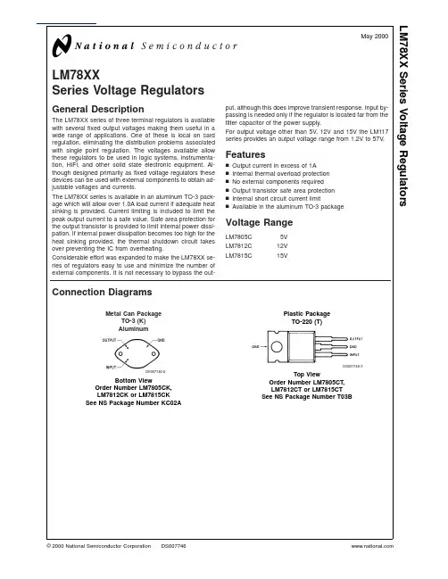
LM78XX
(Note 2) 5V 10V Min 4.8 4.75 Typ Max 5 5.2 Min 11.5 12V 19V Typ Max 12 Min 12.5 14.4 12.6 14.25 15V 23V Typ Max 15 15.6 15.75 V V V mV V mV V mV V mV V mV mV mV mA mA mA mA V mA V µV dB dB V V mΩ
3
LM78XX
Electrical Characteristics LM78XXC
0˚C ≤ TJ ≤ 125˚C unless otherwise noted. Output Voltage Input Voltage (unless otherwise noted) Symbol Parameter Short-Circuit Current Peak Output Current Average TC of VOUT VIN Input Voltage Required to Maintain Line Regulation Tj = 25˚C, IO ≤ 1A Tj = 25˚C Tj = 25˚C 0˚C ≤ Tj ≤ +125˚C, IO = 5 mA Conditions
Voltage Range
LM7805C LM7812C LM7815C 5V 12V 15V
Connection Diagrams
lm7805 限流电阻计算
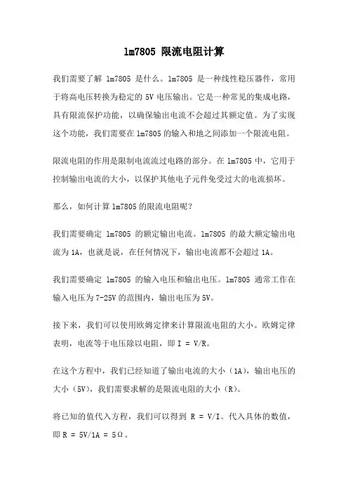
lm7805 限流电阻计算我们需要了解lm7805是什么。
lm7805是一种线性稳压器件,常用于将高电压转换为稳定的5V电压输出。
它是一种常见的集成电路,具有限流保护功能,以确保输出电流不会超过其额定值。
为了实现这个功能,我们需要在lm7805的输入和地之间添加一个限流电阻。
限流电阻的作用是限制电流流过电路的部分。
在lm7805中,它用于控制输出电流的大小,以保护其他电子元件免受过大的电流损坏。
那么,如何计算lm7805的限流电阻呢?我们需要确定lm7805的额定输出电流。
lm7805的最大额定输出电流为1A,也就是说,在任何情况下,输出电流都不会超过1A。
我们需要确定lm7805的输入电压和输出电压。
lm7805通常工作在输入电压为7-25V的范围内,输出电压为5V。
接下来,我们可以使用欧姆定律来计算限流电阻的大小。
欧姆定律表明,电流等于电压除以电阻,即I = V/R。
在这个方程中,我们已经知道了输出电流的大小(1A),输出电压的大小(5V),我们需要求解的是限流电阻的大小(R)。
将已知的值代入方程,我们可以得到R = V/I。
代入具体的数值,即R = 5V/1A = 5Ω。
所以,我们可以得出结论,lm7805的限流电阻应该选择5Ω。
需要注意的是,这个计算结果是基于lm7805的最大额定输出电流为1A的情况下得出的。
如果我们需要输出更大的电流,那么限流电阻的大小也需要相应调整。
还需要考虑限流电阻的功率耗散。
根据功率公式P = IV,我们可以计算出限流电阻的功率耗散。
在lm7805的情况下,输入电压为7-25V,输出电流为1A,限流电阻为5Ω,代入公式计算,可以得到P = 5V × 1A = 5W。
因此,为了保证限流电阻正常工作,我们需要选择一个功率至少为5W的限流电阻。
lm7805的限流电阻计算方法如下:1. 确定lm7805的额定输出电流;2. 确定lm7805的输入电压和输出电压;3. 使用欧姆定律计算限流电阻的大小;4. 考虑限流电阻的功率耗散。
三端稳压7805和7905稳压原理及典型电路

三端稳压7805和7905稳压原理及典型电路2010-08-21 18:02:36| 分类:家电维修| 标签:稳压电压 tj 电路输出|字号大中小订阅7805外形结构电子产品中,常见的三端稳压集成电路有正电压输出的78 ××系列和负电压输出的79××系列。
顾名思义,三端IC是指这种稳压用的集成电路,只有三条引脚输出,分别是输入端、接地端和输出端。
它的样子象是普通的三极管,TO- 220 的标准封装,也有9013样子的TO-92封装。
用78/79系列三端稳压IC来组成稳压电源所需的外围元件极少,电路内部还有过流、过热及调整管的保护电路,使用起来可靠、方便,而且价格便宜。
该系列集成稳压IC型号中的78或79后面的数字代表该三端集成稳压电路的输出电压,如7806表示输出电压为正6V,7909表示输出电压为负9V。
因为三端固定集成稳压电路的使用方便,电子制作中经常采用。
注意事项在实际应用中,应在三端集成稳压电路上安装足够大的散热器(当然小功率的条件下不用)。
当稳压管温度过高时,稳压性能将变差,甚至损坏。
当制作中需要一个能输出1.5A以上电流的稳压电源,通常采用几块三端稳压电路并联起来,使其最大输出电流为N个1.5A,但应用时需注意:并联使用的集成稳压电路应采用同一厂家、同一批号的产品,以保证参数的一致。
另外在输出电流上留有一定的余量,以避免个别集成稳压电路失效时导致其他电路的连锁烧毁。
在78 ** 、79 ** 系列三端稳压器中最常应用的是TO-220 和TO-202 两种封装。
这两种封装的图形以及引脚序号、引脚功能如附图所示。
从正面看①②③引脚从左向右按顺序标注,接入电路时①脚电压高于②脚,③脚为输出位。
如对于78**正压系列,①脚高电位,②脚接地,;对与79**负压系列,①脚接地,②脚接负电压,输出都是③脚。
如附图所示。
此外,还应注意,散热片总是和接地脚相连。
超详细的7805简介与使用说明
7805稳压器
7805是我们最常用到的稳压芯片了,他的使用方便,用很简单的电路即可以输入一个直流稳压电源,他的输出电压恰好为5v,刚好是51系列单片机运行所需的电压,他有很多的系列如ka7805,ads7805,cw7805等,性能有微小的差别,用的最多的还是lm7805,下面我简单的介绍一下他的3个引脚以及用它来构成的稳压电路的资料。
<7805引脚图>
其中1接整流器输出的+电压,2为公共地(也就是负极),3就是我们需要的正5V输出电压了,下面介绍一个简单的7805电路
<lm7805稳压电路>
上图中R1用220Ω,R2用680Ω的这个是用来调节输出电压的。
输出电压公式Uo≈Uxx(1+ R2/R1),此稳压电路可在5~12V稳压范围内实现输出电压连续可调节。
此三端集成稳压集成电路lm7805最大输入电压为35V,输入输出差需保持2V以上,这样该电路中因为稳压器的直流输入电压是正14V,故该稳压电路的最大输出电压为正12V。
此电路的精度一般可达到0.04以上,用lm7805就能满足一般需求了。
7805
::怎样阅读三端稳压块的数据手册by flytigery 2007/05/17本想系统总结一下线性稳压器的各种参数及其意义,想了好久,还是没有头绪,这里打算从7805的数据手册上写的一些参数入手讨论一下各参数的意义。
LM7805是国家半导体开发出来比较成熟,较早的一种线性稳压半导体器件,现在仍然还有很多公司在使用,个人也用得比较多因为很便宜且性能比较稳定。
常提到的三端稳压块7805就是指它了。
拿它作为例子很有代表性。
参数一:输出电压最简单的一个参数,就是稳压器的输出电压,能稳定在多少V,7805输出电压稳定在5V参数二:线性调整率稳压器的输入电压一般都比较宽,在该范围内,输入如果变化输出电压的变化有多大呢?该参数就是描述这种变化的一个参数。
很显然输出电压的变化是越小越好了,一般都是几毫伏。
拿7805作为例子来说吧,参考Data Sheet就可以知道,在常温,输出500mA电流的情况下,输入电压在7~25V之间变化的时候,输出电压的变化典型值为3mV,最大值为50mV参数三:负载调整率负载发生变化时,输出电压也会相应的发生变化,一般是负载越重,输出电压会有所下降,负载越轻输出电压会有所上升。
负载调整率就是反应这种变化的一个量。
看7805的Data Sheet可知,在负载变化在5mA~1.5A时,输出电压的变化范围在10~50mV参数四:静态电流对于线性稳压器来说是一个非常重要的参数。
该电流为驱动大功率调整管所必须的,它不流向负载,而是直接流向地因此该电流是越小越好。
看7805的Data Sheet可知,在负载小于1A的情况下,静态电流为8mA。
为什么要强调负载呢,因为静态电流的大小与负载有关。
参数五:静态电流变化量静态电流大小与负载大小有关,所以在负载发生变化的情况下,静态电流的变化到底有多大?看7805的Data Sheet可知,在负载变化范围在5mA~1A时,静态电流的变化为0.5mA(静态电流增大)参数六:输出噪声电压三端稳压块输出噪声电压都是一些高频噪声(低频噪声被衰减了)看7805的Data Sheet可知,在10Hz~100kHz频率范围内输出噪声电压为40uV参数七:纹波抑制比三端稳压块的另一个非常重要的参数,很多人都不注意它,低频电路可以不关心这个参数,高频电路这个参数就显得非常重要了。
7805引脚图及稳压电路图资料
7805引脚图及稳压电路图资料
2007年10月26日星期五上午 07:48
7805是我们最常用到的稳压芯片了,他的使用方便,用很简单的电路即可以输入一个直流稳压电源,他的输出电压恰好为5v,刚好是51系列单片机运行所需的电压,他有很多的系列如ka7805,ads7805,cw7805等,性能有微小的差别,用的最多的还是lm7805,下面我简单的介绍一下他的3个引脚以及用它来构成的稳压电路的资料。
<7805引脚图>
其中1接整流器输出的+电压,2为公共地(也就是负极),3就是我们需要的正5V输出电压了,下面介绍一个简单的7805电路
<lm7805稳压电路>
上图中R1用220Ω,R2用680Ω的这个是用来调节输出电压的。
输出电压公式Uo≈Uxx(1+R2/R1),此稳压电路可在5~12V稳压范围内实现输出电压连续可调节。
此三端集成稳压集成电路lm7805最大输入电压为35V,输入输出差需保持2V以上,这样该电路中因为稳压器的直流输入电压是正14V,故该稳压电路的最大输出电压为正12V。
此电路的精度一般可达到0.04以上,用lm7805就能满足一般需求了。
L7805AB中文资料
L7800AB/ACSERIESPRECISION 1A REGULATORS®November 1999s OUTPUT CURRENT IN EXCESS OF 1AsOUTPUT VOLTAGESOF 5;6;8;9;12;15;18;20;24Vs THERMAL OVERLOAD PROTECTIONs OUTPUT TRANSITION SOA PROTECTION s 2%OUTPUT VOLTAGE TOLERANCE sGUARANTEED IN EXTENDED TEMPERATURE RANGEDESCRIPTIONThe L7800A series of three-terminal positive regulators is available in TO-220and D 2PAK packages and several fixed output voltages,making it useful in a wide range of applications.These regulators can provide local on-card regulation,eliminating the distribution problems associated with single point regulation.Each type employs internal current limiting,thermal shut-down and safe area protection,making it essentially indestructible.If adequate heat sinking is provided,they can deliver over 1A output current.Although designed primarily as fixed voltage regulators,these devices can be used with external components to obtain adjustable voltages and currents.TO-220D 2PAKBLOCK DIAGRAM1/17CONNECTION DIAGRAM AND ORDERING NUMBERS (top view)TO-220D 2PAKTHERMAL DATASymbolParameterD 2PAK TO-220UnitR thj-ca se R thj-amb Thermal Resistance Junction-case Max Thermal Resistance Junction-ambient Max362.5350o C/W oC/WTypeTO-220D 2PAK (*)Output VoltageL7805AB L7805AC L7806AB L7806AC L7808AB L7808AC L7809AB L7809AC L7812AB L7812AC L7815AB L7815AC L7818AB L7818AC L7820AB L7820AC L7824AB L7824ACL7805ABV L7805ACV L7806ABV L7806ACV L7808ABV L7808ACV L7809ABV L7809ACV L7812ABV L7812ACV L7815ABV L7815ACV L7818ABV L7818ACV L7820ABV L7820ACV L7824ABV L7824ACVL7805ABD2T L7805ACD2T L7806ABD2T L7806ACD2T L7808ABD2T L7808ACD2T L7809ABD2T L7809ACD2T L7812ABD2T L7812ACD2T L7815ABD2T L7815ACD2T5V 5V 6V 6V 8V 8V 9V 9V 12V 12V 15V 15V 18V 18V 24V 24V(*)AVAILABLE IN TAPE AND REEL WITH ”-TR”SUFFIXABSOLUTE MAXIMUM RATINGSSymbol ParameterValue Unit V i DC Input Voltage (for V O =5to 18V)(for V O =20,24V)3540V VI o Output Current Internally limited P tot Power DissipationInternally limitedT op Operating Junction Temperature Range (for L7800AC )(for L7800AB )0to 150-40to 125o C o C T st gStorage Temperature Range-65to 150oCL7800AB/AC2/17L7800AB/AC APPLICATION CIRCUITSCHEMATIC DIAGRAM3/17TEST CIRCUITSFigure3:Ripple Rejection.Figure2:Load Regulation.Figure1:DC Parameter L7800AB/AC4/17*Load and line regulation are specified at constant junction temperature.Changes in V o due to heating effects must be taken into account separately.Pulse testing with low duty cycle is used.ELECTRICAL CHARACTERISTICS FOR L7805A (V i =10V,I o =1A,T j =0to 125o C (L7805AC),T j =-40to 125o C (L7805AB)unless otherwise specified)Symbol ParameterTest ConditionsMin.Typ.Max.Unit V o Output Voltage T j =25o C 4.95 5.1V V o Output Voltage I o =5mA to 1A P o ≤15W V i =7.5to 20V 4.85 5.2V ∆V o *Line RegulationV i =7.5to 25V I o =500mA V i =8to 12V V i =8to 12V T j =25o C V i =7.3to 20VT j =25o C710275052550mV mV mV mV ∆V o *Load RegulationI o =5mA to 1AI o =5mA to 1.5A T j =25o C I o =250to 750mA 2530810010050mV mV mV I d Quiescent Current T j =25oC4.366mA ∆I dQuiescent Current ChangeV i =8to 25V I o =500mAV i =7.5to 20VT j =25o C I o =5mA to 1A 0.80.80.5mA mA mA SVR Supply Voltage Rejection V i =8to 18V f =120HzI o =500mA 68dB V d Dropout Voltage I o =1AT j =25o C2V e N Output Noise Voltage B =10Hz to 100KHz T j =25oC10µV/V o R o Output Resistance f =1KHz 17m ΩI s c Short Circuit Current V i =35V T amb =25o C0.2A I scp Short Circuit Peack Current T j =25o C2.2A ∆V o∆TOutput Voltage Drift-1.1mV/o CL7800AB/AC5/17ELECTRICAL CHARACTERISTICS FOR L7806A(V i=11V,I o=1A,T j=0to125o C(L7806AC),T j=-40to125o C(L7806AB)unless otherwise specified)Symbol Parameter Test Conditions Min.Typ.Max.Unit V o Output Voltage T j=25o C 5.886 6.12V V o Output Voltage I o=5mA to1A P o≤15WV i=8.6to21V5.7666.24V∆V o*Line Regulation V i=8.6to25V I o=500mAV i=9to13VV i=9to13V T j=25o CV i=8.3to21V T j=25o C9113960603060mVmVmVmV∆V o*Load Regulation I o=5mA to1AI o=5mA to1.5A T j=25o CI o=250to750mA 25301010010050mVmVmVI d Quiescent Current T j=25o C 4.366mA∆I d Quiescent Current Change V i=9to25V I o=500mAV i=8.6to21V T j=25o CI o=5mA to1A 0.80.80.5mAmAmASVR Supply Voltage Rejection V i=9to19V f=120HzI o=500mA65dB V d Dropout Voltage I o=1A T j=25o C2Ve N Output Noise Voltage B=10Hz to100KHz T j=25o C10µV/V oR o Output Resistance f=1KHz17mΩI s c Short Circuit Current V i=35V T amb=25o C0.2AI scp Short Circuit Peack Current T j=25o C 2.2A∆V o∆TOutput Voltage Drift-0.8mV/o C*Load and line regulation are specified at constant junction temperature.Changes in V o due to heating effects must be taken into account separately.Pulse testing with low duty cycle is used.L7800AB/AC6/17ELECTRICAL CHARACTERISTICS FOR L7808A(V i=14V,I o=1A,T j=0to125o C(L7808AC),T j=-40to125o C(L7808AB)unless otherwise specified)Symbol Parameter Test Conditions Min.Typ.Max.Unit V o Output Voltage T j=25o C7.8488.16V V o Output Voltage I o=5mA to1A P o≤15WV i=10.6to23V7.788.3V∆V o*Line Regulation V i=10.6to25V I o=500mAV i=11to17VV i=11to17V T j=25o CV i=10.4to23V T j=25o C 121551280804080mVmVmVmV∆V o*Load Regulation I o=5mA to1AI o=5mA to1.5A T j=25o CI o=250to750mA 25301010010050mVmVmVI d Quiescent Current T j=25o C 4.366mA∆I d Quiescent Current Change V i=11to25V I o=500mAV i=10.6to23V T j=25o CI o=5mA to1A 0.80.80.5mAmAmASVR Supply Voltage Rejection V i=11.5to21.5V f=120HzI o=500mA62dB V d Dropout Voltage I o=1A T j=25o C2Ve N Output Noise Voltage B=10Hz to100KHz T j=25o C10µV/V oR o Output Resistance f=1KHz18mΩI s c Short Circuit Current V i=35V T amb=25o C0.2AI scp Short Circuit Peack Current T j=25o C 2.2A∆V o∆TOutput Voltage Drift-0.8mV/o C*Load and line regulation are specified at constant junction temperature.Changes in V o due to heating effects must be taken into account separately.Pulse testing with low duty cycle is used.L7800AB/AC7/17ELECTRICAL CHARACTERISTICS FOR L7809A(V i=15V,I o=1A,T j=0to125o C(L7809AC),T j=-40to125o C(L7809AB)unless otherwise specified)Symbol Parameter Test Conditions Min.Typ.Max.Unit V o Output Voltage T j=25o C8.8299.18V V o Output Voltage I o=5mA to1A P o≤15WV i=10.6to23V8.6599.35V∆V o*Line Regulation V i=10.6to25V I o=500mAV i=11to17VV i=11to17V T j=25o CV i=10.4to23V T j=25o C 121551290904590mVmVmVmV∆V o*Load Regulation I o=5mA to1AI o=5mA to1.5A T j=25o CI o=250to750mA 25301010010050mVmVmVI d Quiescent Current T j=25o C 4.366mA∆I d Quiescent Current Change V i=11to25V I o=500mAV i=10.6to23V T j=25o CI o=5mA to1A 0.80.80.5mAmAmASVR Supply Voltage Rejection V i=11.5to21.5V f=120HzI o=500mA61dB V d Dropout Voltage I o=1A T j=25o C2Ve N Output Noise Voltage B=10Hz to100KHz T j=25o C10µV/V oR o Output Resistance f=1KHz18mΩI s c Short Circuit Current V i=35V T amb=25o C0.2AI scp Short Circuit Peack Current T j=25o C 2.2A∆V o∆TOutput Voltage Drift-0.8mV/o C*Load and line regulation are specified at constant junction temperature.Changes in V o due to heating effects must be taken into account separately.Pulse testing with low duty cycle is used.L7800AB/AC8/17ELECTRICAL CHARACTERISTICS FOR L7812A(V i=19V,I o=1A,T j=0to125o C(L7812AC),T j=-40to125o C(L7812AB)unless otherwise specified)Symbol Parameter Test Conditions Min.Typ.Max.Unit V o Output Voltage T j=25o C11.751212.25V V o Output Voltage I o=5mA to1A P o≤15WV i=14.8to27V11.51212.5V∆V o*Line Regulation V i=14.8to30V I o=500mAV i=16to22VV i=16to22V T j=25o CV i=14.5to27V T j=25o C 131661312012060120mVmVmVmV∆V o*Load Regulation I o=5mA to1AI o=5mA to1.5A T j=25o CI o=250to750mA 25301010010050mVmVmVI d Quiescent Current T j=25o C 4.466mA∆I d Quiescent Current Change V i=15to30V I o=500mAV i=14.8to27V T j=25o CI o=5mA to1A 0.80.80.5mAmAmASVR Supply Voltage Rejection V i=15to25V f=120HzI o=500mA60dB V d Dropout Voltage I o=1A T j=25o C2Ve N Output Noise Voltage B=10Hz to100KHz T j=25o C10µV/V oR o Output Resistance f=1KHz18mΩI s c Short Circuit Current V i=35V T amb=25o C0.2AI scp Short Circuit Peack Current T j=25o C 2.2A∆V o∆TOutput Voltage Drift-1mV/o C*Load and line regulation are specified at constant junction temperature.Changes in V o due to heating effects must be taken into account separately.Pulse testing with low duty cycle is used.L7800AB/AC9/17ELECTRICAL CHARACTERISTICS FOR L7815A(V i=23V,I o=1A,T j=0to125o C(L7815AC),T j=-40to125o C(L7815AB)unless otherwise specified)Symbol Parameter Test Conditions Min.Typ.Max.Unit V o Output Voltage T j=25o C14.71515.3V V o Output Voltage I o=5mA to1A P o≤15WV i=17.9to30V14.41515.6V∆V o*Line Regulation V i=17.9to30V I o=500mAV i=20to26VV i=20to26V T j=25o CV i=17.5to30V T j=25o C 131661315015075150mVmVmVmV∆V o*Load Regulation I o=5mA to1AI o=5mA to1.5A T j=25o CI o=250to750mA 25301010010050mVmVmVI d Quiescent Current T j=25o C 4.466mA∆I d Quiescent Current Change V i=17.5to30V I o=500mAV i=17.5to30V T j=25o CI o=5mA to1A 0.80.80.5mAmAmASVR Supply Voltage Rejection V i=18.5to28.5V f=120HzI o=500mA58dB V d Dropout Voltage I o=1A T j=25o C2Ve N Output Noise Voltage B=10Hz to100KHz T j=25o C10µV/V oR o Output Resistance f=1KHz19mΩI s c Short Circuit Current V i=35V T amb=25o C0.2AI scp Short Circuit Peack Current T j=25o C 2.2A∆V o∆TOutput Voltage Drift-1mV/o C*Load and line regulation are specified at constant junction temperature.Changes in V o due to heating effects must be taken into account separately.Pulse testing with low duty cycle is used.L7800AB/AC10/17ELECTRICAL CHARACTERISTICS FOR L7818A(V i=27V,I o=1A,T j=0to125o C(L7818AC),T j=-40to125o C(L7818AB)unless otherwise specified)Symbol Parameter Test Conditions Min.Typ.Max.Unit V o Output Voltage T j=25o C17.641818.36V V o Output Voltage I o=5mA to1A P o≤15WV i=21to33V17.31818.7V∆V o*Line Regulation V i=21to33V I o=500mAV i=24to30VV i=24to30V T j=25o CV i=20.6to33V T j=25o C 252810518018090180mVmVmVmV∆V o*Load Regulation I o=5mA to1AI o=5mA to1.5A T j=25o CI o=250to750mA 25301010010050mVmVmVI d Quiescent Current T j=25o C 4.566mA∆I d Quiescent Current Change V i=21to33V I o=500mAV i=21to33V T j=25o CI o=5mA to1A 0.80.80.5mAmAmASVR Supply Voltage Rejection V i=22to32V f=120HzI o=500mA57dB V d Dropout Voltage I o=1A T j=25o C2Ve N Output Noise Voltage B=10Hz to100KHz T j=25o C10µV/V oR o Output Resistance f=1KHz19mΩI s c Short Circuit Current V i=35V T amb=25o C0.2AI scp Short Circuit Peack Current T j=25o C 2.2A∆V o∆TOutput Voltage Drift-1mV/o C*Load and line regulation are specified at constant junction temperature.Changes in V o due to heating effects must be taken into account separately.Pulse testing with low duty cycle is used.11/17ELECTRICAL CHARACTERISTICS FOR L7820A(V i=28V,I o=1A,T j=0to125o C(L7820AC),T j=-40to125o C(L7820AB)unless otherwise specified)Symbol Parameter Test Conditions Min.Typ.Max.Unit V o Output Voltage T j=25o C19.62020.4V V o Output Voltage I o=5mA to1A P o≤15WV i=23to35V19.22020.8V∆V o*Line Regulation V i=23to35V I o=500mAV i=26to32VV i=26to32V T j=25o CV i=23to32V T j=25o C 200200100200mVmVmVmV∆V o*Load Regulation I o=5mA to1AI o=5mA to1.5A T j=25o CI o=250to750mA 25301010010050mVmVmVI d Quiescent Current T j=25o C 4.566mA∆I d Quiescent Current Change V i=23to35V I o=500mAV i=23to35V T j=25o CI o=5mA to1A 0.80.80.5mAmAmASVR Supply Voltage Rejection V i=24to35V f=120HzI o=500mA56dB V d Dropout Voltage I o=1A T j=25o C2Ve N Output Noise Voltage B=10Hz to100KHz T j=25o C10µV/V oR o Output Resistance f=1KHz20mΩI s c Short Circuit Current V i=35V T amb=25o C0.2AI scp Short Circuit Peack Current T j=25o C 2.2A∆V o∆TOutput Voltage Drift-1mV/o C*Load and line regulation are specified at constant junction temperature.Changes in V o due to heating effects must be taken into account separately.Pulse testing with low duty cycle is used.12/17ELECTRICAL CHARACTERISTICS FOR L7824A(V i=33V,I o=1A,T j=0to125o C(L7824AC),T j=-40to125o C(L7824AB)unless otherwise specified)Symbol Parameter Test Conditions Min.Typ.Max.Unit V o Output Voltage T j=25o C23.52424.5V V o Output Voltage I o=5mA to1A P o≤15WV i=27.3to38V232425V∆V o*Line Regulation V i=27to38V I o=500mAV i=30to36VV i=30to36V T j=25o CV i=26.7to38V T j=25o C 31351431240240120240mVmVmVmV∆V o*Load Regulation I o=5mA to1AI o=5mA to1.5A T j=25o CI o=250to750mA 25301010010050mVmVmVI d Quiescent Current T j=25o C 4.666mA∆I d Quiescent Current Change V i=27.3to38V I o=500mAV i=27.3to38V T j=25o CI o=5mA to1A 0.80.80.5mAmAmASVR Supply Voltage Rejection V i=28to38V f=120HzI o=500mA54dB V d Dropout Voltage I o=1A T j=25o C2Ve N Output Noise Voltage B=10Hz to100KHz T j=25o C10µV/V oR o Output Resistance f=1KHz20mΩI s c Short Circuit Current V i=35V T amb=25o C0.2AI scp Short Circuit Peack Current T j=25o C 2.2A∆V o∆TOutput Voltage Drift-1.5mV/o C*Load and line regulation are specified at constant junction temperature.Changes in V o due to heating effects must be taken into account separately.Pulse testing with low duty cycle is used.13/17APPLICATIONS INFORMATIONDESIGN CONSIDERATIONSThe L7800A Series of fixed voltage regulators are designed with Thermal Overload Protection that shuts down the circuit when subjected to an excessive power overload condition,Internal Short-circuit Protection that limits the maximum current the circuit will pass,and Output Transistor Safe-Area Compensation that reduces the output short-circuit current as the voltage across the pass transistor is increased.In many low current applications,compensation capacitors are not required.However,it is recommended that the regulator input be bypassed with a capacitor if the regulator is connected to the power supply filter with long wire lengths,or if the output load capacitance is large.An input bypass capacitor should be selected to provide good high-frequency characteristics to insure stable operation under all load conditions.A 0.33µF or larger tantalum,mylar,or other capacitor having low internal impedance at high frequencies should be chosen.The bypass capacitor should be mounted with the shortest possible leads directly across the regulators input terminals.Normally good construction techniques should be used to minimize ground loops and lead resistance drops since the regulator has no external sense lead.Figure 4:Current Regulator.Figure 5:Adjustable Output Regulator.Figure 6:Current Boost Regulator.Figure 7:Short-circuit Protection.V O ,7.0V to 20V V i –V O ≥2.0VThe addition of an operational amplifier allows adjustment to higher or intermediate values while retaining regulation characteristics.The minimum voltage obtainable with this arrangement is 2.0V greater than the regulator voltage.The circuit of figure 6can be modified to provide supply protection against short circuit by adding a short-circuit sense resistor,R sc ,and an additional PNP transistor.The current sensing PNP must be able to handle the short-circuit current of the three-terminal regulator.Therefore,a four-ampere plastic power transistor is specified.R 1=V BEQ 1I REQ −I Q 1βQ 1I O =IREG+Q 1(I REG −V BEQ 1R 1)I O =V XXR 1+I d 14/17DIM.mminch MIN.TYP.MAX.MIN.TYP.MAX.A 4.40 4.600.1730.181C 1.23 1.320.0480.051D 2.402.720.0940.107D1 1.270.050E 0.490.700.0190.027F 0.610.880.0240.034F1 1.14 1.700.0440.067F2 1.14 1.700.0440.067G 4.95 5.150.1940.203G1 2.4 2.70.0940.106H210.010.400.3930.409L216.40.645L413.014.00.5110.551L5 2.65 2.950.1040.116L615.2515.750.6000.620L7 6.2 6.60.2440.260L9 3.5 3.930.1370.154DIA.3.75 3.850.1470.151L6ACDED 1FGL7L2Dia.F 1L5L4H 2L9F 2G 1TO-220MECHANICAL DATAP011C15/17DIM.mminch MIN.TYP.MAX.MIN.TYP.MAX.A 4.4 4.60.1730.181A1 2.49 2.690.0980.106B 0.70.930.0270.036B2 1.14 1.70.0440.067C 0.450.60.0170.023C2 1.23 1.360.0480.053D 8.959.350.3520.368E 1010.40.3930.409G 4.88 5.280.1920.208L 1515.850.5900.624L2 1.27 1.40.0500.055L31.41.750.0550.068L2L3LB2B GEAC2DCA1DETAIL”A”DETAIL”A”A 2P011P6/FTO-263(D 2PAK)MECHANICAL DATA16/17Information furnished is believed to be accurate and reliable.However,STMicroelectroni c s assumes no responsibility for the consequences of use of such information nor for any infringement of patents or other rights of third parties which may result from its use.No license is granted by implication or otherwise under any patent or patent rights of STMicroelectroni c s.Specification mentioned in this publication are subject to change without notice.This publication supersedes and replaces all informati o n previously supplied.STMicroelectronics products are not authorized for use as critical components in life support devices or systems withoutexpress written approval of STMicroelectronics.The ST logo is a registered trademark of STMicroelectronics©1999STMicroelectronics–Printed in Italy–All Rights ReservedSTMicroelectronics GROUP OF COMPANIESAustralia-Brazil-China-Finland-France-Germany-Hong Kong-India-Italy-Japan-Malaysia-Malta-MoroccoSingapore-Spain-Sweden-Switzerland-United Kingdom-U.S.A..17/17。
- 1、下载文档前请自行甄别文档内容的完整性,平台不提供额外的编辑、内容补充、找答案等附加服务。
- 2、"仅部分预览"的文档,不可在线预览部分如存在完整性等问题,可反馈申请退款(可完整预览的文档不适用该条件!)。
- 3、如文档侵犯您的权益,请联系客服反馈,我们会尽快为您处理(人工客服工作时间:9:00-18:30)。
7V≤VI≤20V
TJ=25℃, 7V≤VI≤25V
ΔVO
电压调整率*
1V≤VI≤12V
9
100
gTJ=25℃, 5.0mA≤IO≤1.5A
ΔVO
负载调整率*
4
pmV
50
TJ=25℃, 250mA≤IO≤750mA
IQ
静态电流
5.0
f8
mA
TJ=25℃
. 0.03
0.5
. RθJC——热阻(结到壳)……………………………… 5℃/W w RθJA——热阻(结到空气)………………………… 65℃/W
TOPR——工作结温范围…………………………… 0~125℃
ww TSTG——贮存温度范围………………………… -65~150℃
█ 功能框图
1
海纳电子资讯网:www.fpga-arm.com
H 7805
█ 应用电路(续)
.
m
r
a
- 图 8、大电流稳压器
a
图 7、可调整输出稳压器(7~30V)
g
p
f
.
图 10、跟踪稳压器
w
w
w 图 9、带短路保护的大电流输出
图 12、负输出电压电路
图 11、分离电源(±15V-1A)
图 13、开关稳压器
4
海纳电子资讯网:www.fpga-arm.com
H 7805
█ 典型特性曲线
静态电流
峰值输出电流
m.
r
输出电流(A)
静态电流(mA)
a
-
a
g
结温(℃)
p 输入-输出电压差(V)
输出电压
f
静态电流
.
w
静态电流(mA)
w
w
归一化输出电压(V)
结温(℃)
输入电压(V)
5
w
注: 1)输出电压对应于“XX”值。输入电压,即
w
使是纹波电压中的低值点,都必须高于所需 输出电压 2V 以上。
2)当稳压器远离电源滤波器时,要求用 C1。
3)CO 可改善稳定性和瞬态响应。
图 4、固定输出稳压器
图 5、恒流源
图 6、提高输出电压电路
3
海纳电子资讯网:www.fpga-arm.com
TO-220
m
路,但使用外接元件,可获得不同的电压和电流。
r
█ 主要特点
a
输出电流可达 1A 输出电压有:5V 过热保护
1―输入,INPUT
- 2―地,GND a3―输出,OUTPUT
短路保护 输出晶体管 SOA 保护
pg
█ 极限值(Ta=25℃)
f
VI——输入电压(VO=5~18V)…………………………… 35V
RO
输出阻抗
15
mΩ f=1kHz
ISC
短路电流
230
mA VI=35V, TA=25℃
IPK
峰值电流
2.2
A
TJ=25℃
2
海纳电子资讯网:www.fpga-arm.com
H 7805
█ 测试电路
.
m
r
a
图 1、DC 参数测试
- 图 2、负载调整率测试
a
g
p
█ 应用电路
.f 图 3、纹波抑制比测试 w
5mA≤IO≤1.0A
ΔIQ
静态电流变化率
w0.3
1.3
mA 7V≤VI≤25V
ΔVO/ΔT 输出电压温度系数
w -0.8
mV/℃ IO=5mA
VN
w 输出噪声电压
42
μV TA=25℃, 10Hz≤f≤100kHz
RR
纹波抑制比
62
73
dB f=120Hz, 8V≤VI≤18V
VD
下降电压
2
V
IO=1A, TJ=25℃
海纳电子资讯网:www.fpga-arm.com
3-TERMINAL FIXED VOLTAGE REGULATOR
H 7805
对应国外型号 KA7805
█ 概述
█ 外形图及引脚排列
H 7805 系列为 3 端正稳压电路,TO-220 封装,能提供多
.
种固定的输出电压,应用范围广。内含过流、过热和过载保 护电路。带散热片时,输出电流可达 1A。虽然是固定稳压电
H 7805
(参见测试电路,除非另有说明,0℃≤TJ≤125℃,IO=500mA,VI=10V,CI=0.33μF,CO=0.1μF)
. 参数符号 符 号 说 明 最小值 典型值 最大值 单 位
测试条件
-arm VO
输出电压
4.8
5.0
5.2
4.75
5.0
5.25
4.0
100
TJ=25℃
V
5.OmA≤IO≤1.0A, PD≤15W,