A Fully Integrated Touch Screen Controller Based on 12Bit 825kSps SAR ADC
全数字电源设计
ADC
S/H
Reference
反馈
Rf1 Rf2
© 2014 Microchip Technology Incorporated.版权所有。
Microchip dsPIC® DSC
C15L12 APS
幻灯片 6
III型补偿器 (原极点 + 两个零点/极点对)
步骤1:确定系统传递函数
f p2 = f ESR
建立 闭环控制系统
– 电压模式 –
谐振频率fR下的双极点
交叉 频率fX
开关频率的 一半fSW/2
G(s) x H(s) 执行器 补偿器
ESR 频率fESR
© 2014 Microchip Technology Incorporated.版权所有。
二阶系统(电压模式控制下的降压转换器)
C15L12 APS
Zf
=1 s ⋅C2
(R2
+
s
1 ⋅ C1
)
Zi
= R1
1 s ⋅C2
步骤2:确定系统极点和零点
Gain (dB)
f z1 = 0.6 ⋅ fLC
f p0
90
Phase (o)
90
© 2014 Microchip Technology Incorporated.版权所有。
C15L12 APS
幻灯片 7
累加器
数字III型(3p3z)补偿器的线性差分方程
© 2014 Microchip Technology Incorporated.版权所有。
C15L12 APS
幻灯片 9
课程安排
回顾数字补偿器 用于优化电源转换器的非线性控制方法 功率因数校正改善 高级8位电源示例
基于ARM的触摸屏控制模板
基于ARM的触摸屏控制摘要:本文介绍了基于ARM的触摸屏控制的设计思路、原理和实现方法。
硬件电路主要由PHILIPS公司的ARM7TDMI-S微控制器LPC2290,FM7843控制器和SID13503控制器构成。
利用C语言编写驱动和用户程序,通过触摸屏的FM7843控制器将触摸信号进行A/D转换,进而利用ARM芯片和彩色液晶屏SID13503控制器,将触摸动作在液晶屏上进行显示,最终实现了触摸屏和液晶屏的控制。
该设计操作直观、简单、功耗小、提高了人机交互的友好性。
关键词:触摸屏; 液晶屏; ARMThe Control of Touch-screen Based on ARMAbstract: This paper introduced the designing of thought and the achievement methods of the control of ARM touch-screen based on ARM. The hardware circuit consists of ARM7TDMI-S LPC2290 controller, FM7843 controller and SID13503 controller which are all produced by PHILIPS Corporation. The researchers compose driven and user program in C language ,and utilize FM7843 controller of the touch-screen to proceed A/D converter, then use ARM chips and SID13503 controller of LCD screen to show the action of touching on the LCD screen, ultimately realize the control of touch-screen and LCD screen. This design is direct-viewing、simple、as well as costs less power and can improve the friendliness of human-computer interaction.Key word: touch-screen; LCD;ARM目录摘要 (1)1 引言 (3)2 总体设计 (3)3 硬件设计部分 (3)3.1 彩色液晶显示器 (3)3.2 彩色液晶屏驱动电路及SID13503控制器 (4)3.3 触摸屏原理 (5)3.4 触摸屏驱动电路及FM7843控制器 (5)4 软件设计部分 (6)4.1 触摸屏驱动程序设计 (6)4.2 彩色液晶屏驱动程序设计 (8)4.3 用户程序 (11)5总结 (13)参考文献 (14)附录一 (15)附录二 (18)附录三 (22)附录四 (26)1 引言随着信息产业的迅猛发展,由于触摸屏操作直观、简单、功耗小、有利于提高人机交互的友好性等优点,而逐渐取代鼠标、键盘,在人机交互中成为主要输入设备[1]。
ADC122S051中文资料
ADC122S1012Channel,1MSPS 12-Bit A/D ConverterGeneral DescriptionThe ADC122S101is a low-power,two-channel CMOS 12-bit analog-to-digital converter with a high-speed serial interface.Unlike the conventional practice of specifying performance at a single sample rate only,the ADC122S101is fully speci-fied over a sample rate range of 500kSPS to 1MSPS.The converter is based on a successive-approximation register architecture with an internal track-and-hold circuit.It can be configured to accept one or two input signals at inputs IN1and IN2.The output serial data is straight binary,and is compatible with several standards,such as SPI ™,QSPI ™,MICROW-IRE,and many common DSP serial interfaces.The ADC122S101operates with a single supply that can range from +2.7V to +5.25V.Normal power consumption using a +3V or +5V supply is 4.3mW and 13.1mW,respec-tively.The power-down feature reduces the power consump-tion to just 0.14µW using a +3V supply,or 0.32µW using a +5V supply.The ADC122S101is packaged in an 8-lead MSOP package.Operation over the industrial temperature range of −40˚C to +85˚C is guaranteed.Featuresn Specified over a range of sample rates.n Two input channelsn Variable power managementnSingle power supply with 2.7V -5.25V rangeKey Specificationsn DNL +0.9/−0.6LSB (typ)n INL ±0.64LSB (typ)n SNR72.4dB (typ)nPower Consumption —3V Supply 4.3mW (typ)—5V Supply13.1mW (typ)Applicationsn Portable Systemsn Remote Data Acquisitionn Instrumentation and Control SystemsPin-Compatible Alternatives by Resolution and SpeedAll devices are fully pin and function compatible.ResolutionSpecified for Sample Rate Range of:50to 200kSPS200to 500kSPS 500kSPS to 1MSPS12-bit ADC122S021ADC122S051ADC122S10110-bit ADC102S021ADC102S051ADC102S1018-bitADC082S021ADC082S051ADC082S101Connection Diagram20125205Ordering InformationOrder Code Temperature Range Description Top Mark ADC122S101CIMM −40˚C to +85˚C 8-Lead MSOP PackageX24C ADC122S101CIMMX −40˚C to +85˚C8-Lead MSOP Package,Tape &ReelX24CADC122S101EVALEvaluation BoardTRI-STATE ®is a trademark of National Semiconductor Corporation QSPI ™and SPI ™are trademarks of Motorola,Inc.April 2005ADC122S1012Channel,1MSPS 12-Bit A/D Converter©2005National Semiconductor Corporation Block Diagram20125207Pin Descriptions and Equivalent CircuitsPin No.SymbolDescriptionANALOG I/O5,4IN1and IN2Analog inputs.These signals can range from 0V to V A .DIGITAL I/O8SCLK Digital clock input.This clock directly controls the conversion and readout processes.7DOUT Digital data output.The output samples are clocked out of this pin on falling edges of the SCLK pin.6DIN Digital data input.The ADC122S101’s Control Register is loaded through this pin on rising edges of the SCLK pin.1CSChip select.On the falling edge of CS,a conversion process begins.Conversions continue as long as CS is held low.POWER SUPPLY2V APositive supply pin.This pin should be connected to a quiet +2.7V to +5.25V source and bypassed to GND with a 1µF capacitor and a 0.1µF monolithic capacitor located within 1cm of the power pin.3GNDThe ground return for the analog supply and signals.A D C 122S 101 2Absolute Maximum Ratings(Notes1,2) If Military/Aerospace specified devices are required, please contact the National Semiconductor Sales Office/ Distributors for availability and specifications.Analog Supply Voltage V A−0.3V to6.5V Voltage on Any Pin to GND−0.3V to V A+0.3V Input Current at Any Pin(Note3)±10mA Package Input Current(Note3)±20mA Power Consumption at T A=25˚C See(Note4) ESD Susceptibility(Note5)Human Body Model Machine Model 2500V 250VJunction Temperature+150˚C Storage Temperature−65˚C to+150˚C Operating Ratings(Notes1,2)Operating Temperature Range−40˚C≤T A≤+85˚C V A Supply Voltage+2.7V to+5.25V Digital Input Pins Voltage Range−0.3V to V A Clock Frequency0.8MHz to16MHz Analog Input Voltage0V to V APackage Thermal ResistancePackageθJA8-lead MSOP250˚C/WSoldering process must comply with National Semiconduc-tor’s Reflow Temperature Profile specifications.Refer to /packaging.(Note6)ADC122S101Converter Electrical Characteristics(Note9)The following specifications apply for V A=+2.7V to5.25V,GND=0V,f SCLK=8MHz to16MHz,f SAMPLE=500kSPS to1 MSPS,C L=35pF unless otherwise noted.Boldface limits apply for T A=T MIN to T MAX:all other limits T A=25˚C.Symbol Parameter Conditions TypicalLimits(Note7)UnitsSTATIC CONVERTER CHARACTERISTICSResolution with No Missing Codes12BitsINL Integral Non-Linearity +0.64+1.6LSB(max)−0.64−1.2LSB(min)DNL Differential Non-Linearity +0.9+1.6LSB(max)−0.6−1.0LSB(min)V OFF Offset Error+0.44±1.3LSB(max)OEM Channel to Channel Offset ErrorMatch±0.1±1.0LSB(max)FSE Full-Scale Error−0.34±1.5LSB(max)FSEM Channel to Channel Full-Scale ErrorMatch±0.1±1.0LSB(max)DYNAMIC CONVERTER CHARACTERISTICSSINAD Signal-to-Noise Plus Distortion Ratio V A=+2.7to5.25V,f IN=40.3kHz,−0.02dBFS7269.2dB(min)SNR Signal-to-Noise Ratio V A=+2.7to5.25Vf IN=40.3kHz,−0.02dBFS72.470.6dB(min)THD Total Harmonic Distortion V A=+2.7to5.25V,f IN=40.3kHz,−0.02dBFS−82−75dB(max)SFDR Spurious-Free Dynamic Range V A=+2.7to5.25Vf IN=40.3kHz,−0.02dBFS8376dB(min)ENOB Effective Number of Bits V A=+2.7to5.25V11.711.2Bits(min)Channel-to-Channel Crosstalk V A=+5.25Vf IN=40.3kHz−86dBIMD Intermodulation Distortion,SecondOrder TermsV A=+5.25V,f a=40.161kHz,f b=41.015kHz−87dB Intermodulation Distortion,ThirdOrder TermsV A=+5.25Vf a=40.161kHz,f b=41.015kHz−88dBFPBW-3dB Full Power Bandwidth V A=+5V11MHzV A=+3V8MHzADC122S101 3ADC122S101Converter Electrical Characteristics(Note 9)(Continued)The following specifications apply for V A =+2.7V to 5.25V,GND =0V,f SCLK =8MHz to 16MHz,f SAMPLE =500kSPS to 1MSPS,C L =35pF unless otherwise noted.Boldface limits apply for T A =T MIN to T MAX :all other limits T A =25˚C.SymbolParameterConditionsTypicalLimits (Note 7)UnitsANALOG INPUT CHARACTERISTICS V IN Input Range 0to V AVI DCL DC Leakage Current ±0.02±1µA (max)C INAInput CapacitanceTrack Mode 33pF Hold Mode 3pFDIGITAL INPUT CHARACTERISTICS V IH Input High Voltage V A =+5.25V 2.4V (min)V A =+3.6V2.1V (min)V IL Input Low Voltage 0.8V (max)I IN Input CurrentV IN =0V or V IN =V A±0.1±10µA (max)C INDDigital Input Capacitance24pF (max)DIGITAL OUTPUT CHARACTERISTICS V OH Output High Voltage I SOURCE =200µA V A −0.03V A −0.5V (min)I SOURCE =1mA V A −0.1VV OL Output Low VoltageI SINK =200µA 0.020.4V (max)I SINK =1mA0.1VI OZH ,I OZL TRI-STATE ®Leakage Current ±0.01±1µA (max)C OUTTRI-STATE ®Output Capacitance 24pF (max)Output CodingStraight (Natural)BinaryPOWER SUPPLY CHARACTERISTICS (C L =10pF)V AAnalog Supply Voltage2.7V (min)5.25V (max)I ASupply Current,Normal Mode (Operational,CS low)V A =+5.25Vf SAMPLE =1MSPS,f IN =40.3kHz 2.5 3.0mA (max)V A =+3.6V,f SAMPLE =1MSPS,f IN =40.3kHz 1.2 1.6mA (max)Supply Current,Shutdown (CS high)V A =+5.25Vf SAMPLE =0kSPS 60nA V A =+3.6V,f SAMPLE =0kSPS 38nA P DPower Consumption,Normal Mode (Operational,CS low)V A =+5.25V 13.115.8mW (max)V A =+3.6V 4.3 5.8mW (max)Power Consumption,Shutdown (CS high)V A =+5.25V 0.32µW V A =+3.6V0.14µW AC ELECTRICAL CHARACTERISTICS f SCLK Maximum Clock Frequency (Note 8)8MHz (min)16MHz (max)f S Sample Rate (Note 8)500kSPS (min)1MSPS (max)t CONV Conversion Time 13SCLK cycles DC SCLK Duty Cyclef SCLK =16MHz 5030%(min)70%(max)t ACQTrack/Hold Acquisition Time Full-Scale Step Input3SCLK cycles Throughput TimeAcquisition Time +Conversion Time16SCLK cyclesA D C 122S 101 4ADC122S101Timing SpecificationsThe following specifications apply for V A=+2.7V to5.25V,GND=0V,f SCLK=8MHz to16MHz,f SAMPLE=500kSPS to1 MSPS,C L=35pF,Boldface limits apply for T A=T MIN to T MAX:all other limits T A=25˚C.Symbol Parameter Conditions TypicalLimits(Note7)Unitst CSU Setup Time SCLK High to CS Falling Edge(Note10)V A=+3.0V−3.510ns(min) V A=+5.0V−0.5t CLH Hold time SCLK Low to CS Falling Edge(Note10)V A=+3.0V+4.510ns(min) V A=+5.0V+1.5t EN Delay from CS Until DOUT active V A=+3.0V+430ns(max) V A=+5.0V+2t ACC Data Access Time after SCLK Falling Edge V A=+3.0V+14.530ns(max) V A=+5.0V+13t SU Data Setup Time Prior to SCLK Rising Edge+310ns(min) t H Data Valid SCLK Hold Time+310ns(min)t CH SCLK High Pulse Width 0.5xt SCLK0.3xt SCLKns(min)t CL SCLK Low Pulse Width 0.5xt SCLK0.3xt SCLKns(min)t DIS CS Rising Edge to DOUT High-Impedance Output FallingV A=+3.0V 1.820ns(max)V A=+5.0V 1.3Output RisingV A=+3.0V 1.0V A=+5.0V 1.0Note1:Absolute Maximum Ratings indicate limits beyond which damage to the device may occur.Operating Ratings indicate conditions for which the device is functional,but do not guarantee specific performance limits.For guaranteed specifications and test conditions,see the Electrical Characteristics.The guaranteed specifications apply only for the test conditions listed.Some performance characteristics may degrade when the device is not operated under the listed test conditions.Note2:All voltages are measured with respect to GND=0V,unless otherwise specified.Note3:When the input voltage at any pin exceeds the power supply(that is,V IN<GND or V IN>V A),the current at that pin should be limited to10mA.The20mA maximum package input current rating limits the number of pins that can safely exceed the power supplies with an input current of10mA to two.The Absolute Maximum Rating specification does not apply to the V A pin.The current into the V A pin is limited by the Analog Supply Voltage specification.Note4:The absolute maximum junction temperature(T J max)for this device is150˚C.The maximum allowable power dissipation is dictated by T J max,thejunction-to-ambient thermal resistance(θJA),and the ambient temperature(T A),and can be calculated using the formula P D MAX=(T J max−T A)/θJA.The valuesfor maximum power dissipation listed above will be reached only when the device is operated in a severe fault condition(e.g.when input or output pins are drivenbeyond the power supply voltages,or the power supply polarity is reversed).Obviously,such conditions should always be avoided.Note5:Human body model is100pF capacitor discharged through a1.5kΩresistor.Machine model is220pF discharged through zero ohms.Note6:Reflow temperature profiles are different for lead-free and non-lead-free packages.Note7:Tested limits are guaranteed to National’s AOQL(Average Outgoing Quality Level).Note8:This is the frequency range over which the electrical performance is guaranteed.The device is functional over a wider range which is specified under Operating Ratings.Note9:Datasheet min/max specification limits are guaranteed by design,test,or statistical analysis.Note10:Clock may be in any state(high or low)when CS is asserted,with the restrictions on setup and hold time given by t CSU and t CLH.ADC122S1015Timing Diagrams20125251ADC122S101Operational Timing Diagram20125208Timing Test Circuit20125206ADC122S101Serial Timing Diagram20125250SCLK and CS Timing ParametersA D C 122S 101 6Specification DefinitionsACQUISITION TIME is the time required to acquire the input voltage.That is,it is time required for the hold capacitor to charge up to the input voltage.APERTURE DELAY is the time between the fourth falling SCLK edge of a conversion and the time when the input signal is acquired or held for conversion.CONVERSION TIME is the time required,after the input voltage is acquired,for the ADC to convert the input voltage to a digital word.CROSSTALK is the coupling of energy from one channel into the other channel,or the amount of signal energy from one analog input that appears at the measured analog input.DIFFERENTIAL NON-LINEARITY (DNL)is the measure of the maximum deviation from the ideal step size of 1LSB.DUTY CYCLE is the ratio of the time that a repetitive digital waveform is high to the total time of one period.The speci-fication here refers to the SCLK.EFFECTIVE NUMBER OF BITS (ENOB,or EFFECTIVE BITS)is another method of specifying Signal-to-Noise and Distortion or SINAD.ENOB is defined as (SINAD −1.76)/6.02and says that the converter is equivalent to a perfect ADC of this (ENOB)number of bits.FULL POWER BANDWIDTH is a measure of the frequency at which the reconstructed output fundamental drops 3dB below its low frequency value for a full scale input.GAIN ERROR is the deviation of the last code transition (111...110)to (111...111)from the ideal (V REF −1.5LSB),after adjusting for offset error.INTEGRAL NON-LINEARITY (INL)is a measure of the deviation of each individual code from a line drawn from negative full scale (1⁄2LSB below the first code transition)through positive full scale (1⁄2LSB above the last code transition).The deviation of any given code from this straight line is measured from the center of that code value.INTERMODULATION DISTORTION (IMD)is the creation of additional spectral components as a result of two sinusoidal frequencies being applied to the ADC input at the same time.It is defined as the ratio of the power in the second and third order intermodulation products to the sum of the power in both of the original frequencies.IMD is usually expressed in dB.MISSING CODES are those output codes that will never appear at the ADC outputs.The ADC122S101is guaranteed not to have any missing codes.OFFSET ERROR is the deviation of the first code transition (000...000)to (000...001)from the ideal (i.e.GND +0.5LSB).SIGNAL TO NOISE RATIO (SNR)is the ratio,expressed in dB,of the rms value of the input signal to the rms value of the sum of all other spectral components below one-half the sampling frequency,not including harmonics or d.c.SIGNAL TO NOISE PLUS DISTORTION (S/N+D or SINAD)Is the ratio,expressed in dB,of the rms value of the input signal to the rms value of all of the other spectral compo-nents below half the clock frequency,including harmonics but excluding d.c.SPURIOUS FREE DYNAMIC RANGE (SFDR)is the differ-ence,expressed in dB,between the rms values of the input signal and the peak spurious signal where a spurious signal is any signal present in the output spectrum that is not present at the input,excluding d.c.TOTAL HARMONIC DISTORTION (THD)is the ratio,ex-pressed in dB or dBc,of the rms total of the first five harmonic components at the output to the rms level of the input signal frequency as seen at the output.THD is calcu-lated aswhere A f1is the RMS power of the input frequency at the output and A f2through A f6are the RMS power in the first 5harmonic frequencies.THROUGHPUT TIME is the minimum time required between the start of two successive conversion.It is the acquisition time plus the conversion time.In the case of the ADC122S101,this is 16SCLK periods.ADC122S1017Typical Performance CharacteristicsT A =+25˚C,f SAMPLE =500kSPS to 1MSPS,f SCLK =8MHzto 16MHz,f IN =40.3kHz unless otherwise stated.DNL -V A =3.0VINL -V A =3.0V2012522020125221DNL -V A =5.0V INL -V A =5.0V2012526220125263DNL vs.Supply INL vs.Supply2012522220125223A D C 122S 101 8Typical Performance Characteristics T A =+25˚C,f SAMPLE =500kSPS to 1MSPS,f SCLK =8MHz to16MHz,f IN =40.3kHz unless otherwise stated.(Continued)DNL vs.Clock FrequencyINL vs.Clock Frequency2012522420125225DNL vs.Clock Duty Cycle INL vs.Clock Duty Cycle2012522620125227DNL vs.Temperature INL vs.Temperature2012522820125229ADC122S1019Typical Performance Characteristics T A =+25˚C,f SAMPLE =500kSPS to 1MSPS,f SCLK =8MHz to16MHz,f IN =40.3kHz unless otherwise stated.(Continued)SNR vs.SupplyTHD vs.Supply2012523020125235SNR vs.Clock Frequency THD vs.Clock Frequency2012523120125236SNR vs.Clock Duty Cycle THD vs.Clock Duty Cycle2012523220125237A D C 122S 101 10Typical Performance Characteristics T A =+25˚C,f SAMPLE =500kSPS to 1MSPS,f SCLK =8MHz to16MHz,f IN =40.3kHz unless otherwise stated.(Continued)SNR vs.Input FrequencyTHD vs.Input Frequency2012523320125238SNR vs.Temperature THD vs.Temperature2012523420125239SFDR vs.Supply SINAD vs.Supply2012524020125245ADC122S10111Typical Performance Characteristics T A =+25˚C,f SAMPLE =500kSPS to 1MSPS,f SCLK =8MHz to16MHz,f IN =40.3kHz unless otherwise stated.(Continued)SFDR vs.Clock FrequencySINAD vs.Clock Frequency2012524120125246SFDR vs.Clock Duty Cycle SINAD vs.Clock Duty Cycle2012524220125247SFDR vs.Input Frequency SINAD vs.Input Frequency2012524320125248A D C 122S 101 12Typical Performance Characteristics T A =+25˚C,f SAMPLE =500kSPS to 1MSPS,f SCLK =8MHz to16MHz,f IN =40.3kHz unless otherwise stated.(Continued)SFDR vs.TemperatureSINAD vs.Temperature2012524420125249ENOB vs.Supply ENOB vs.Clock Frequency2012525220125253ENOB vs.Clock Duty Cycle ENOB vs.Input Frequency2012525420125255ADC122S10113Typical Performance Characteristics T A =+25˚C,f SAMPLE =500kSPS to 1MSPS,f SCLK =8MHz to16MHz,f IN =40.3kHz unless otherwise stated.(Continued)ENOB vs.TemperatureSpectral Response -3V,500kSPS2012525620125259Spectral Response -5V,500kSPS Spectral Response -3V,1MSPS2012526020125264Spectral Response -5V,1MSPS Power Consumption vs.Throughput2012526520125261A D C 122S 101 14Applications Information1.0ADC122S101OPERATIONThe ADC122S101is a successive-approximation analog-to-digital converter designed around a charge-redistribution digital-to-analog converter.Simplified schematics of the ADC122S101in both track and hold modes are shown in Figures 1,2,respectively.In Figure 1,the ADC122S101is in track mode:switch SW1connects the sampling capacitor to one of two analog input channels through the multiplexer,and SW2balances the comparator inputs.The ADC122S101is in this state for the first three SCLK cycles after CS is brought low.Figure 2shows the ADC122S101in hold mode:switch SW1connects the sampling capacitor to ground,maintaining thesampled voltage,and switch SW2unbalances the compara-tor.The control logic then instructs the charge-redistribution DAC to add fixed amounts of charge to the sampling capaci-tor until the comparator is balanced.When the comparator is balanced,the digital word supplied to the DAC is the digital representation of the analog input voltage.The ADC122S101is in this state for the fourth through sixteenth SCLK cycles after CS is brought low.The time when CS is low is considered a serial frame.Each of these frames should contain an integer multiple of 16SCLK cycles,during which time a conversion is performed and clocked out at the DOUT pin and data is clocked into the DIN pin to indicate the multiplexer address for the next conversion.2.0USING THE ADC122S101An ADC122S101timing diagram and a serial interface timing diagram for the ADC122S101are shown in the Timing Dia-grams section.CS is chip select,which initiates conversions and frames the serial data transfers.SCLK (serial clock)controls both the conversion process and the timing of serial data.DOUT is the serial data output pin,where a conversion result is sent as a serial data stream,MSB first.Data to be written to the ADC122S101’s Control Register is placed on DIN,the serial data input pin.New data is written to DIN with each conversion.A serial frame is initiated on the falling edge of CS and ends on the rising edge of CS.Each frame must contain an integer multiple of 16rising SCLK edges.The ADC output data (DOUT)is in a high impedance state when CS is high and is active when CS is low.Thus,CS acts as an output enable.Additionally,the device goes into a power down state when CS is high and also between continuous conversion cycles.During the first 3cycles of SCLK,the ADC is in the track mode,acquiring the input voltage.For the next 13SCLK cycles the conversion is accomplished and the data is clocked out,MSB first,starting on the 5th clock.If there are more than one conversion in a frame,the ADC will re-enter the track mode on the falling edge of SCLK after the N*16th rising edge of SCLK,and re-enter the hold/convert mode on the N*16+4th falling edge of SCLK,where "N"is an integer.When CS is brought high,SCLK is internally gated off.If SCLK is stopped in the low state while CS is high,the subsequent fall of CS will generate a falling edge of the internal version of SCLK,putting the ADC into the track mode.This is seen by the ADC as the first falling edge of SCLK.If SCLK is stopped with SCLK high,the ADC enters the track mode on the first falling edge of SCLK after the falling edge of CS.During each conversion,data is clocked into the DIN pin on the first 8rising edges of SCLK after the fall of CS.For each20125209FIGURE 1.ADC122S101in Track Mode20125210FIGURE 2.ADC122S101in Hold ModeADC122S10115Applications Information(Continued)conversion,it is necessary to clock in the data indicating the input that is selected for the conversion after the current one.See Tables 1,2and Table 3.If CS and SCLK go low simultaneously,it is the following rising edge of SCLK that is considered the first rising edge for clocking data into DIN.There are no power-up delays or dummy conversions re-quired with the ADC122S101.The ADC is able to sample and convert an input to full conversion immediately following power up.The first conversion result after power-up will be that of IN1.TABLE 1.Control Register BitsBit 7(MSB)Bit 6Bit 5Bit 4Bit 3Bit 2Bit 1Bit 0DONTCDONTCADD2ADD1ADD0DONTCDONTCDONTCTABLE 2.Control Register Bit DescriptionsBit #:Symbol:Description7-6,2-0DONTC Don’t care.The value of these bits do not affect the device.3ADD0These three bits determine which input channel will be sampled and converted in the next track/hold cycle.The mapping between codes and channels is shown in Table 3.4ADD15ADD2TABLE 3.Input Channel SelectionADD2ADD1ADD0Input Channel x 00IN1(Default)x 01IN2x1xNot allowed.The output signal at the D OUTpin is indeterminate if ADD1is high.A D C 122S 101 16Applications Information(Continued)3.0ADC122S101TRANSFER FUNCTIONThe output format of the ADC122S101is straight binary.Code transitions occur midway between successive integerLSB values.The LSB width for the ADC122S101is V A /4096.The ideal transfer characteristic is shown in Figure 3.The transition from an output code of 000000000000to a code of 000000000001is at 1/2LSB,or a voltage of V A /8192.Other code transitions occur at steps of one LSB.4.0TYPICAL APPLICATION CIRCUITA typical application of the ADC122S101is shown in Figure 4.Power is provided in this example by the National Semi-conductor LP2950low-dropout voltage regulator,available in a variety of fixed and adjustable output voltages.The power supply pin is bypassed with a capacitor network located close to the ADC122S101.Because the reference for the ADC122S101is the supply voltage,any noise on the supplywill degrade device noise performance.To keep noise off the supply,use a dedicated linear regulator for this device,or provide sufficient decoupling from other circuitry to keep noise off the ADC122S101supply pin.Because of the ADC122S101’s low power requirements,it is also possible to use a precision reference as a power supply to maximize performance.The four-wire interface is also shown con-nected to a microprocessor or DSP .20125211FIGURE 3.Ideal Transfer Characteristic20125213FIGURE 4.Typical Application CircuitADC122S10117Applications Information(Continued)5.0ANALOG INPUTSAn equivalent circuit for one of the ADC122S101’s input channels is shown in Figure 5.Diodes D1and D2provide ESD protection for the analog inputs.At no time should any input go beyond (V A +300mV)or (GND −300mV),as these ESD diodes will begin conducting,which could result in erratic operation.The capacitor C1in Figure 5has a typical value of 3pF,and is mainly the package pin capacitance.Resistor R1is the on resistance of the multiplexer and track /hold switch,and is typically 500ohms.Capacitor C2is the ADC122S101sam-pling capacitor and is typically 30pF.The ADC122S101will deliver best performance when driven by a low-impedance source to eliminate distortion caused by the charging of the sampling capacitance.This is especially important when using the ADC122S101to sample AC signals.Also important when sampling dynamic signals is a band-pass or low-pass filter to reduce harmonics and noise,improving dynamic performance.6.0DIGITAL INPUTS AND OUTPUTSThe ADC122S101’s digital output DOUT is limited by,and cannot exceed,the supply voltage,V A .The digital input pins are not prone to latch-up and,and although not recom-mended,SCLK,CS and DIN may be asserted before V A without any latch-up risk.7.0POWER SUPPLY CONSIDERATIONSThe ADC122S101is fully powered-up whenever CS is low,and fully powered-down whenever CS is high,with one exception:the ADC122S101automatically enters power-down mode between the 16th falling edge of a conversion and the 1st falling edge of the subsequent conversion (see Timing Diagrams).The ADC122S101can perform multiple conversions back to back;each conversion requires 16SCLK cycles.The ADC122S101will perform conversions continuously as long as CS is held low.The user may trade off throughput for power consumption by simply performing fewer conversions per unit time.The Power Consumption vs.Sample Rate curve in the Typical Performance Curves section shows the typical power con-sumption of the ADC122S101versus throughput.To calcu-late the power consumption,simply multiply the fraction of time spent in the normal mode by the normal mode power consumption ,and add the fraction of time spent in shutdown mode multiplied by the shutdown mode power dissipation.7.1Power ManagementWhen the ADC122S101is operated continuously in normal mode,the maximum throughput is f SCLK /16.Throughput may be traded for power consumption by running f SCLK at its maximum 16MHz and performing fewer conversions per unit time,putting the ADC122S101into shutdown mode between conversions.A plot of typical power consumption versus throughput is shown in the Typical Performance Curves section.To calculate the power consumption for a given throughput,multiply the fraction of time spent in the normal mode by the normal mode power consumption and add the fraction of time spent in shutdown mode multiplied by the shutdown mode power consumption.Generally,the user will put the part into normal mode and then put the part back into shutdown mode.Note that the curve of power consumption vs.throughput is nearly linear.This is because the power consumption in the shutdown mode is so small that it can be ignored for all practical purposes.7.2Power Supply Noise ConsiderationsThe charging of any output load capacitance requires cur-rent from the power supply,V A .The current pulses required from the supply to charge the output capacitance will cause voltage variations on the supply.If these variations are large enough,they could degrade SNR and SINAD performance of the ADC.Furthermore,discharging the output capaci-tance when the digital output goes from a logic high to a logic low will dump current into the die substrate,which is resis-tive.Load discharge currents will cause "ground bounce"noise in the substrate that will degrade noise performance if that current is large enough.The larger is the output capaci-tance,the more current flows through the die substrate and the greater is the noise coupled into the analog channel,degrading noise performance.To keep noise out of the power supply,keep the output load capacitance as small as practical.If the load capacitance is greater than 35pF,use a 100Ωseries resistor at the ADC output,located as close to the ADC output pin as practical.This will limit the charge and discharge current of the output capacitance and improve noise performance.20125214FIGURE 5.Equivalent Input CircuitA D C 122S 101 18。
HTRC11001资料
• RFID systems. 3 GENERAL DESCRIPTION
HITAG(1) is the family name of the reader chip HTRC11001T to use with transponders which are based on the HITAG tag ICs (HT1ICS3002x or HT2ICS2002x).
RX
14
SYNCHRONOUS DEMODULATOR
BANDPASS FILTER AMPLIFIER DYNAMIC CONTROL DIGITIZER
PHASE MEASUREMENT CONTROL REGISTER 13 QGND 12 CEXT 1 VSS
HTRC11001T
5 MODE
HTRC11001T
control input to enable filtering of serial clock and data input; for active antenna applications oscillator input 1 oscillator input 2 serial clock input of microcontroller interface serial data input of microcontroller interface serial data output of microcontroller interface not connected high-pass filter coupling capacitor connection internal analog virtual ground capacitor connection demodulator input
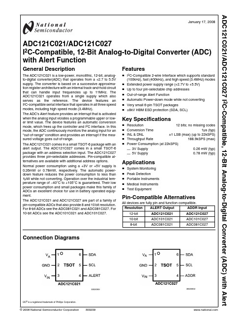
ADC081C021资料
FeaturesБайду номын сангаас
■ I2C-Compatible 2-wire Interface which supports standard
(100kHz), fast (400kHz), and high speed (3.4MHz) modes
■ Extended power supply range (+2.7V to +5.5V) ■ Up to four pin-selectable chip addresses ■ Out-of-range Alert Function ■ Automatic Power-down mode while not converting ■ Very small 6-pin TSOT packages ■ ±8kV HBM ESD protection (SDA, SCL)
■ Power Consumption (at 22kSPS)
— 3V Supply
0.26 mW (typ)
— 5V Supply
0.78 mW (typ)
Applications
■ System Monitoring ■ Peak Detection ■ Portable Instruments ■ Medical Instruments ■ Test Equipment
The ADC's Alert feature provides an interrupt that is activated when the analog input violates a programmable upper or lower limit value. The device features an automatic conversion mode, which frees up the controller and I2C interface. In this mode, the ADC continuously monitors the analog input for an "out-of-range" condition and provides an interrupt if the measured voltage goes out-of-range.
AD转换芯片介绍

l???????ADS7812?低功耗串行12位采样模数转换器
l???????ADS7810?12位800kHz采样CMOS模数转换器
l???????ADS7800?12位3us采样模数转换器
l???????ADS574??兼容微处理器的采样CMOSA/D转换器?
l???????THS1007?10位6MSPS同步采样四路通道ADC;包含并行DSP/uPI/F通道自动扫描?
l???????ADS901??10位20MSPSADC,具有单端/差动输入、外部参考和可调节全范围?
l???????ADS900??10位20MSPSADC,具有单端/差动输入、内部基准和可调节全范围?
l???????ADS822?10位40MSPSADC,具有单端/差动输入、内/外基准和断电、引脚符合ADS823/6/8?
l???????ADS821?10位40MSPSADC,单端/差动输入具有内部基准和9.3位ENOB?
l???????ADS820?10位20MSPSADC,单端/差动输入具有内部基准和9.5位ENOB?
l???????TLC3545?14位200KSPSADC,具有串行输出、自动断电和伪差动输入?
l???????TLC3544?14位、5V、200KSPS、4通道单级性ADC
l???????TLC3541?14位200KSPSADC系列输出、自动断电、单端输入?
l???????THS1403?14位、3MSPSADC单通道、差动输入、DSP/uPIF、可编程增益放大器、内部S&H?
l???????TLC4541?16位200KSPSADC,具有串行输出、自动断电和单端输入
S32K 培训资料 单片机介绍
KFA family, rev A
Carl Culshaw, Systems Engineering, Automotive MCU
Oct 24.2014
TM
Confidential and Proprietary
Complex Safety Function
(e.g. EPS)
Simple Safety Function
(e.g. Airbag)
ASIL D target ASIL C target ASIL B target ASIL A target
EPS, ESP, Engine Vision based Management ADAS… MCU HEV… HW
(10.9 Safety Element out of Context)
SafeAssure Standard HW Airbag, Body, DIS…
(8.13 Qualification of Hardware Components)
Enabled for ISO 26262
Where we enable the customer to do the Qualification, testing and analysis to prove that our component is suitable for the purpose of his safety concept.
8
Functional Safety
Single Point Fault Metric
• •
Diversity of safety levels
STM32F103RB数据手册
Medium-density performance line ARM-based 32-bit MCU with 64 or 128 KB Flash, USB, CAN, 7 timers, 2 ADCs, 9 communication interfaces
■ ■
VFQFPN36 6 × 6 mm
LQFP48 7 × 7 m LQFP100 14 × 14 m LQFP64 10 × 10 m
BGA100 10 × 10 mm BGA64 5 × 5 mm
■
Debug mode – Serial wire debug (SWD) & JTAG interfaces 7 timers – Three 16-bit timers, each with up to 4 IC/OC/PWM or pulse counter and quadrature (incremental) encoder input – 16-bit, motor control PWM timer with deadtime generation and emergency stop – 2 watchdog timers (Independent and Window) – SysTick timer: a 24-bit downcounter Up to 9 communication interfaces – Up to 2 x I2C interfaces (SMBus/PMBus) – Up to 3 USARTs (ISO 7816 interface, LIN, IrDA capability, modem control) – Up to 2 SPIs (18 Mbit/s) – CAN interface (2.0B Active) – USB 2.0 full-speed interface CRC calculation unit, 96-bit unique ID Packages are ECOPACK® Device summary
迪文科技DWIN Technology EKT043B产品数据手册说明书
EKT043B产品特点:●基于T5L0芯片,运行DGUS II系统,开发板。
● 4.3寸,480*800分辨率,262K色,IPS屏,宽视角。
●电容触摸屏。
● 2.54mm间距焊盘引脚,引出用户CPU核的IO、UART、CAN、AD、PWM等接口,二次开发十分方便。
Features:●Based on T5L0,running DGUS II system,Development board.● 4.3-inch,480*800Pixels resolution,262K Colors,IPS-TFT-LCD,Wide viewing angle.●Capacitive touch screen.● 2.54mm pitch pad pins,including IO,UART,CAN,AD and PWM from user CPU core for easysecondary development.硬件及接口Hardware and interface1.1硬件接口图Hardware interface硬件接口图Hardware interface1.2接口说明Interface description序号No.名称Name说明Description1T5L0芯片T5L0ASIC迪文自主研发,2020年量产,1MBytes片内Nor Flash,其中512KBytes用于存储用户数据库,擦写次数>100,000次Developed by DWIN.Mass production in2020,1MBytes Nor Flash on thechip,512KBytes used to store the user database.Rewrite cycle:over100,000times2液晶屏接口LCM interfaceFPC40_0.5mm,RGB接口FPC40_0.5mm,RGB interface3电容触摸屏接口CTP interface6Pin_0.5mm,IIC接口6Pin_0.5mm,IIC interface4USB接口USB interfaceUSB供电接口,可选择UART1USB power supply interface,option UART15Flash 16MBytes NOR Flash,存放字库、图片、音乐文件,擦写次数>100,000次16MBytes NOR Flash,for fonts,pictures and audio files.Rewrite cycle:over100,000times6扬声器接口Speaker interface2Pin_2.0座子,连接扬声器2Pin_2.0socket,Connect to speaker7SD卡接口SD interfaceFAT32格式,下载文件,文件可在屏幕统计显示,下载速率:4Mb/sFAT32.Download files by SD interface can be displayed in statistics.Download rate:4Mb/s8WIFI模块WIFI moduleWIFI模块:可连接到云平台实现远程更新Wi-Fi module:connect to the cloud platform to update remotely9HME05接口HME05interface连接T5L的JTAG接口,在Keil开发环境下进行代码IAP调试和仿真运行Connect the JTAG interface of T5L for code IAP debugging and simulationoperation in KEIL development environment10选择短接Short circuit通过跳线帽选择USB/WIFI、JTAG/IO P#35-38、GUI/OS JATGOption USB/WIFI,JTAG/IO P#35-38,GUI/OS JATG function with jumper.11GUI/OS CPU引出接口GUI/OS CPU pinGUI/OS CPU引出接口,丝印在另外一面Pin of GUI/OS CPU with screen printing on the other side12供电接口Power supplyinterface6-36V宽压供电接口6-36V wide voltage power supply interface1.32.54mm间距焊盘引脚定义Pin definition of2.54mm pitch land pattern管脚序号Pin NO.定义Definition说明Description备注Remark1P1.0I/O口2P1.1I/O口3P1.2I/O口4P1.3I/O口5P1.4I/O口6P1.5I/O口7P1.6I/O口8P1.7I/O口9P2.0I/O口10P2.1I/O口11P2.2I/O口12P2.3I/O口13P2.4I/O口14P2.5I/O口15P2.6I/O口16P2.7I/O口17P3.0I/O口18P3.1I/O口19P3.2I/O口20P3.3I/O口21ADC1AD输入22ADC0AD输入23ADC3AD输入24ADC2AD输入25PWM216bit PWM输出26ADC4AD输入27ADC6AD输入28ADC5AD输入29PWM116bit PWM输出30ADC7AD输入31PWM316bit PWM输出32PWM016bit PWM输出33RX3/232UATR3数据接收/RS232 34TX3/232UATR3数据输出/RS232 35RX3/TTL UATR3数据接收/TTL 36TX3/TTL UATR3数据输出/TTL 37TX2/232UATR2数据输出/RS232 38RX2/232UATR2数据接收/RS232 39TX2/TTL UATR2数据输出/TTL 40RX2/TTL UATR2数据接收/TTL 41GND公共接地端42GND公共接地端43UART5/485B UART5数据输出/RS485 44UART5/485A UART5数据接收/RS485 45UART4/485B UART4数据输出/RS485 46UART4/485A UART4数据接收/RS485 47CANH CAN接口数据接收48CANL CAN接口数据输出2、规格参数Specification parameters 2.1显示参数Display parameters显示屏类型LCD TypeIPS,TFT LCD视角Viewing Angle 宽视角,典型值85°/85°/85°/85°(L/R/U/D)Wide viewing angle,85°/85°/85°/85°(L/R/U/D)分辨率Resolution 480×800(支持0°/90°/180°/270°显示模式)480×800pixels(0°/90°/180°/270°)色彩Color 18位6R6G6B 18-bit6R6G6BAA区Active Area(A.A.)93.60mm(W)×56.16mm(H) VA区View Area(V.A.)94.00mm(W)×56.56mm(H)背光模式Backlight ModeLED背光寿命Backlight Service Life >20000小时(以最高亮度连续工作,亮度减半时间)>20000hours(Time of the brightness decaying to50%on the condition of continuous working with the maximum brightness)背光亮度Brightness250nit背光调节Brightness Control 100级亮度调节(当亮度调节至最高亮度的1%~30%时,可能出现闪烁现象,不建议在此范围使用)0~100grade(When the brightness is adjusted to1%~30%of the maximum brightness,flickering may occur and is not recommended to use in this range)注:超过30分钟长时间显示高对比度静止画面可能导致显示残影,请增加屏保避免该问题。
AD9253 14-bit 125 MSPS Four-Channel ADC Reference
连接/参考器件电路笔记 CN-0249Circuits from the Lab™ reference circuits are engineered and tested for quick and easy system integration to help solve today’s analog, mixed-signal, and RF design challenges. For more information and/or support, visit /CN0249.AD9253 14位、125 MSPS 四通道模数转换器(ADC)14位、125 MSPS 四通道ADC ,通过后端数字求和增强SNR 性能Rev. 0Circuits from the Lab™ circuits from Analog Devices have been designed and built by Analog Devices engineers. Standard engineering practices have been employed in the design and construction of each circuit, and their function and performance have been tested and veri ed in a lab environment at room temperature. However , you are solely responsible for testing the circuit and determining its suitability and applicability for your use and application. Accordingly , in no event shall Analog Devices be liable for direct, indirect, special, incidental, consequential or punitive damages due to any cause whatsoever connected to the use of any Circuits from the Lab circuits. (Continued on last page)One Technology Way, P.O. Box 9106, Norwood, MA 02062-9106, U.S.A. Tel: 781.329.4700 Fax: 781.461.3113 ©2013 Analog Devices, Inc. All rights reserved.ADC 1,2,3,4:AD9253QUAD 14-BIT,125MSPSANALOG SIGNAL INPUTnn + 210303-001CLOCK INPUTADC 1ADC 3ADC 4ADC 2POST DIGITAL SUMMERΣnnnANALOG FRONT-ENDCLOCK CIRCUITRY图1. 四个并联ADC 求和得到更高SNR 的基本框图评估和设计支持设计和集成文件原理图、布局文件、物料清单电路功能与优势图1所示电路是14位、125 MSPS 四通道ADC 系统的简化图,该电路使用后端数字求和将信噪比(SNR)从单通道ADC 的74 dBFS 提升到四通道ADC 的78.5 dBFS 。
- 1、下载文档前请自行甄别文档内容的完整性,平台不提供额外的编辑、内容补充、找答案等附加服务。
- 2、"仅部分预览"的文档,不可在线预览部分如存在完整性等问题,可反馈申请退款(可完整预览的文档不适用该条件!)。
- 3、如文档侵犯您的权益,请联系客服反馈,我们会尽快为您处理(人工客服工作时间:9:00-18:30)。
A Fully Integrated Touch Screen Controller Based on 12b 825kS/s SAR ADC
Stefano Pietri, Alfredo Olmos, Michael BerensFreescale Semiconductor 6501 William Cannon Dr. Austin, Texas 78735, USA Andre Vilas Boas, Marcos GoesFreescale SemiconductorRod. Anhanguera, km 104 Campinas - SP - Brazil
Abstract - This paper describes a low-power 12 bits 825kS/s Suc-cessive Approximation Register Analog to Digital Converter (SARADC) for personal digital assistants, portable instruments, andtouch-screen monitor applications. The proposed SAR ADC isbased on 3-stage 4-4-4 C-DAC architecture and a high-speed 3-stages comparator. It features 8 general-purpose input channelsand 8 dedicated channels supporting 4, 5, 7, and 8-wire resistivetouch-screen panels. It has a full-scale input range, power-downmode for low current consumption, and a novel pen-touch detec-tion control with fast response able to support any touch-screenpanel. The ADC performs ±1.3 LSB DNL and ±5 LSB INL whentested up to 125C at supply voltages ranging from 2.7V to 3.6V.Fabricated in a 0.13um CMOS with fringe capacitors, it occupiesan area of 0.17 mm2 and has a total dissipation of 200uA at full
speed. The circuit has been integrated on Freescale MCF5227xMicro-Controller Unit (MCU) family of devices with a 166 MHzColdFire(R) core processor and an LCD controller.
Keywords - SAR ADC, DAC, Successive Approximation, touch screen, pen-touch detection.
I. INTRODUCTIONLonger battery life and new features are expected at everynew generation of portable electronic appliances. The means toincrease active device time are many, from advanced powermanagement, to system on chip integration to limit powerhungry off chip communications. Analog IC designers arechallenged to reduce cost and power budget, still meeting orimproving performance. Considering that analog componentdo not scale with the new CMOS technology, the challengebecomes even more demanding. The SuccessiveApproximation Register Analog to Digital Converter (SARADC) is a family of data converter, known to be second best inclass for each single specification [1-10], therefore widelyreusable in most applications and preferred for the ones thatrequire reasonable speed/performance trade off with low powerconsumption and small silicon area.A resistive touch screen is a sensor that translates thephysical location of a touch at a point in a panel area intovoltages that represents the X and Y coordinates of the touch.Many LCD modules come equipped with resistive touchscreens, which may use 4 wires, 5 wires, 7 wires, or 8 wires for
generating screen bias voltages and reading the touch pointvoltage [11]. In the past, reading touch coordinates from aresistive touch screen required MCU bandwidth or an externaldedicated touch screen controller device, an ADC and severalswitches. Cost saving requirements led to dedicated MCU’sthat integrate on-chip ADC, touch screen biasing circuitry andtouch screen controller that allow to perform position readingson a panel without loading the CPU and without requiringboard components. In this paper the design of a low power, area effective 12bits SAR ADC for a touch-screen application is presented. Thetouch-screen interface to ADC is described in Section 2.Results of high-level model simulation of the CapacitiveDigital to Analog Converter (C-DAC) array are reported inSection 3. Section 4 depicts the high-speed comparator, andthen silicon results are described in Section 5, followed byconclusions in Section 6.
II. TOUCH-SCREEN INTERFACE TO ADCThe analog section of the touch screen interface isillustrated in Fig. 1 and includes all circuitry required to controland read touch position on almost all kinds of touch paneldevices: bias network, input multiplexer, reference multiplexer,12 bit DAC, and comparator. The SAR control block notshown in Fig. 1 implements the function of successiveapproximation data conversion and provides the data to theCPU by means of a dedicated asynchronous communicationchannel.The ADC block can be used as a touch screen or genericpurpose ADC. It can also perform single-ended or ratiometricconversions. Single-ended conversions consume less powerfrom battery because the screen excitation voltage can beswitched-off once the signal is acquired. Ratiometricconversions use the screen excitation voltage as reference forthe ADC. They provide greater accuracy since voltage dropacross switches has no effect. No matter if the block is configured as touch screencontroller or generic purpose ADC, its behavior can bedescribed by a sequence of operations such as: (a) Pen detection phase: the period to detect the pen down state;(b) X measurement phase: the period to take the X coordinatemeasurement; (c) Y measurement phase: the period to take the