CAT808低电压检测芯片
ec800m低功耗at指令

ec800m低功耗at指令摘要:1.引言2.ec800m 低功耗AT 指令简介3.ec800m 低功耗AT 指令的优势4.ec800m 低功耗AT 指令的应用场景5.总结正文:引言:随着物联网技术的不断发展,越来越多的设备需要低功耗、长待机、高性能的特点。
ec800m 是一款支持低功耗AT 指令的芯片,能够满足这些需求,使得设备在保持高性能的同时,降低能耗。
ec800m 低功耗AT 指令简介:ec800m 是一款支持低功耗AT 指令的芯片,其采用先进的低功耗技术,通过降低工作电压和时钟频率,实现低功耗待机。
同时,ec800m 支持AT 指令,使得设备可以通过简单的AT 指令进行远程控制和配置,大大简化了设备的开发和应用。
ec800m 低功耗AT 指令的优势:1.低功耗:ec800m 芯片采用低功耗技术,待机功耗低,满足长待机需求。
2.高性能:在低功耗的同时,ec800m 保持了高性能,满足设备的高速运行需求。
3.远程控制:支持AT 指令,方便设备远程控制和配置。
4.简化开发:通过AT 指令,可以简化设备的开发和应用,降低开发成本。
ec800m 低功耗AT 指令的应用场景:1.物联网设备:如智能家居、智能农业、智能医疗等领域的设备,需要长时间待机,且需要远程控制和配置。
2.通信设备:如GPRS/3G/4G 等无线通信模块,需要低功耗待机,以延长电池寿命。
3.工业控制:如智能工厂、自动化生产线等场景,需要低功耗、高性能的控制设备。
总结:ec800m 低功耗AT 指令芯片凭借其低功耗、高性能、远程控制等优势,在物联网、通信、工业控制等领域有着广泛的应用。
常用8脚开关电源芯片

常用8脚开关电源芯片开关电源芯片是电源管理中常见的一种电源管理IC,它通过开关控制电源的开关状态,使得输入电源能够连接到输出负载部分,从而实现对电源的稳定输出和管理。
常用的8脚开关电源芯片有很多种,下面主要介绍其中的几种。
1. LM317LM317是一种调整型电位技术电源芯片,它可以提供1.2V到37V的可调电源输出,并且在负载变化时能够自动调节输出电压。
它的输入电压可以高达40V,最大输出电流为1.5A。
2. LM7805LM7805是一种固定输出电压的线性稳压器,它的输出电压为5V,并且具有较高的输出电流和低的静态功耗。
它的输入电压范围为7V到35V,最大输出电流为1A。
3. LM2596LM2596是一种可调的开关稳压器,它可以在输入电压范围为4.5V到40V时提供可调的输出电压。
它的输出电流最大可以达到3A,具有较高的效率和稳定性。
4. UC3842UC3842是一种常用的开关电源控制芯片,它具有宽的输入电压范围和高的开关频率。
它可以实现对开关管的开关控制,从而实现对输出电流和电压的精确调节。
5. TNY264TNY264是一种集成开关电源控制器,它具有较高的开关频率和低的静态功耗。
它可以实现对输入电压和输出电压的控制,适用于广泛的应用场景。
6. XL4015XL4015是一种高效率的降压型开关稳压器,它可以通过PWM(脉宽调制)控制实现对输出电压的可调。
它的输入电压范围为8V到32V,最大输出电流为5A。
7. MP2307MP2307是一种高效率的降压型开关稳压器,它可以在输入电压范围为4.75V到23V时提供可调的输出电压。
它的最大输出电流为3A。
8. TS4950TS4950是一种高性能的音频功率放大器,它具有低的静态功耗和低的失真。
它可以在输入电压范围为2.7V到5.5V时提供可调的输出功率。
总结:以上介绍了常见的8脚开关电源芯片,它们在不同的工作场景和应用中具有不同的特点和优势。
HE5080E赫尔半导体

概要:HE 5080E是一款5V USB 适配器输入,高精度双节锂离子电池充电管理芯片。
具有0V 充电功能,涓流充电、恒流充电、恒压充电和自动截止、自动再充等一套完整充电循环的充电管理芯片。
芯片内部特设 9V 抗浪涌,芯片应用更安全可靠。
HE 5080E标准浮充电压为 8.40V,其底部带有散热片接地的 ESOP8 封装,极其精简的外部器件,使得HE 5080E 成为便携式双节锂锂电池充电应用的理想选择。
HE 5080E适合 USB 适配器或其它 5V适配器工作,极大降低了外部配件成本。
当输入电压(USB 电源或 AC 适配器)被拿掉时,HE 5080E自动进入低电流状态,将电池的漏电流降至 1uA 以内。
HE 5080E其它特点包括:欠压闭锁、自适应适配器、自动再充以及一个 LED 充电状态指示引脚等。
封装形式:ESOP8L 标准封装描述:z 10W ,2A 输入异步开关升压充电z 升压充电效率90%z 自动调节输入电流,匹配所有适配器z 支持LED 充电状态指示z 内置功率MOS ,精简外围电路z 600Khz 开关频率,可支持2.2uH 电感z 内置输出过压、短路保护z 内置输入欠压、过压保护z内置IC 过温保护zESD 4KV 静电防护应用:z 蓝牙音箱z 电子烟z 对讲机z成人用品典型应用图:HE 5080E典型应用图HE 5080E双节锂电池HE 5080E双节锂电池串联升压充电管理引脚排列及管脚定义:功能框图管脚序号管脚名称输入/输出功能说明1VIN 输入电源输入脚,外接5V 电源正极2AGND 地数字地3LX输入内部功率MOS 漏极输入端,外接功率电感和二极管4VBS 输出外接BOOST 升压输出端,外接升压输出和滤波电容5BAT 输出充电输出端,外接一颗滤波电容和双节锂电池6ICHG 输入充电电流控制端口,外部通过电阻与地相接,可设置充电电流。
7VSEN 输入VIN 电压检测与Shutdown 复用引脚,当VSEN 达到或低于1.2V 阈值自动降低充电电流;当VSEN 低于0.4V 时,关断充电电路8STAT 输出充电状态指示端口,内部开漏输出,外接状态指示灯和限流电阻ThermalPGND地功率地,需大面积良好接地和散热参数描述数值单位VDD无信号输入时供电电源电压‐0.3~8.0VLX内部功率MOS漏极输入端耐压‐0.3~20V VBS,BAT VBS,BAT引脚耐压极限‐0.3~10VVI输入引脚耐压‐0.3~VDD+0.3V Other PIN其他引脚耐压‐0.3~6.0VTJ结工作温度范围‐40~150℃TSDR引脚温度(焊接10秒)260℃TSTG存储温度范围‐65~150℃θJA封装热阻‐‐‐>芯片到环境热阻(ESOP8封装)40℃/W HBM ESD人体静电模式±4KV HMM ESD机械静电模式±4KV注意事项:1.上述参数仅仅是器件工作的极限值,不建议器件的工作条件超过此极限值,否则会对器件的可靠性和寿命产生影响,甚至造成永久性损坏。
AT8001 用于背光驱动领域的高效率驱动芯片
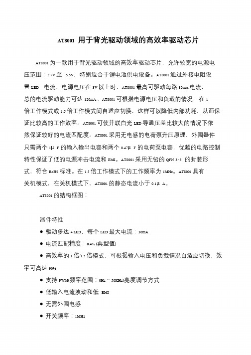
AT8001 用于背光驱动领域的高效率驱动芯片
AT8001 为一款用于背光驱动领域的高效率驱动芯片,允许较宽的电源电压范围:2.7V 至 5.5V,特别适合于锂电池供电设备。
AT8001 通过外接电阻设置LED 电流,电源电压在3V 以上时,AT8001 最高可驱动每路30mA 电流,总的电流驱动能力可达120mA。
AT8001 可根据电源电压和负载的情况,在1 倍工作模式或1.5 倍工作模式间自适应切换,这样可以降低内部功耗,从而保证比较高的工作效率。
AT8001 可使并联白光LED 导通压差比较大的情况下依然保证较好的电流匹配度。
AT8001 采用无电感的电荷泵升压原理,外围器件只需两个1μF的输入输出电容和两个0.47μF的电荷泵电容,优越的电路控制特性保证了低的电源冲击电流和EMI。
AT8001 采用无铅的QFN 3×3的封装形式,符合RoHS 标准。
在1.5 倍工作模式下的工作频率为1MHz。
AT8001 具有关机模式,在关机模式下,AT8001 的静态电流小于0.1μA。
AT8001 的结构框图:
器件特性
●驱动多达4 LED,每个LED 最大电流:30mA
●电流匹配精度:0.4% (典型值)
●高效率的1 倍/1.5 倍模式,可根据输入电压和负载情况自适应切换,效率可高达90%
●支持PWM(频率范围:0Hz~50KHz)亮度调节方式
●低输入电流波动和低EMI
●无需外围电感
●开关频率:1MHz。
别克英朗c0800方向控制模块电源电路低电压

别克英朗c0800方向控制模块电源电路低电压
别克英朗C0800方向控制模块电源电路低电压问题是指车辆的方向盘控制模块无法正常工作,出现电源电路低电压的情况。
以下是对该问题的解释:
C0800是指方向盘控制模块通讯故障码,通常情况下,这种故障码是由于方向盘控制模块出现问题所导致的。
该模块通常由一个控制电路和一个电源电路组成。
电源电路是指方向盘控制模块的供电系统,通常由电池和发电机提供电源。
如果电池电压过低或发电机输出电压异常,方向盘控制模块就会出现电源电路低电压的问题。
造成电源电路低电压的原因可能是电池老化或电池线路接触不良,也可能是发电机故障或发电机线路开路等原因。
此外,电路中的连接器和保险丝也可能引起电路短路等问题。
为了解决这个问题,需要进行一系列诊断测试,如检查电池电压、发电机输出电压、电路连接器和保险丝是否正常,以确定问题的根源。
根据检测结果,可以进行相应的修理和更换。
总之,C0800方向控制模块电源电路低电压问题是由多种因素引起的,需要进行详细的诊断和维修,以确保车辆的正常运转。
交直流两用计量芯片HLW8112
下表是 HLW8112 电路模块经直流校准后的测量数据,PGA = 1,输入 DC 电压 12V,最 大测量电流 3A,采样电阻 25mR 的测试数据:
从两个表可以看出,PGA = 1 的线性比较好,建议在使用直流测量时,优先使用 PGA = 1 倍。
交直流两用计量芯片 HLW8112
芯片介绍
HLW8112 是一款高精度的电能计量 IC,它采用 CMOS 制造工艺,该器件内部 集成了三个∑-Δ型 ADC 和一个高精度的电能计量内核。
HLW8112 主要用于单相应用,也可以测量直流信号。 HLW8112 可以通过多种通讯接口访问片内寄存器,包括 SPI 和 UART。 HLW8112 电能计量 IC 采用 3.3V 或 5.0V 电源供电,内置振荡器,采用 16 脚 SSOP 封装。
入范围是
±800mV/PGA
5
VP
模拟输入 电压信号正输入端,电压的最大输入范围是
±800mV/PGA
6
GND
芯片地 芯片地
7
REF
数字输入 基准电压的输入/输出引脚,需要外接 0.1uFf
去藕电容
8
SDO/TX 数字输出 SPI 数据输出口
UART 数据输出口
9
SDI/RX 数字输入 SPI 数据输入口
+3.3V
DC-DC
+3.3V
DC
1 IAP
VDD 16
2 IAN
INT2 15
3 IBP
CLKO/INT1 14
4 IBN HLW8112 CLKI 13
SSOP16 5 VP
SPIEN 12
6 GND 7 VREF 8 SDO/TX
SCSN 11 SCLK 10 SDI/RX 9
北京集创北方 ICN8201 低功耗电容感应芯片 说明书
概述- 1 -北京集创北方科技有限公司版本号0.2 2011-04ICN8201是一款低功耗电容感应芯片。
芯片包含一个多路开关,实现电容感应、模拟前端和ADC 到管脚的连接;同时包含SPI 串行接口作为控制和通信接口。
芯片性能卓越,不需要修调即对温度、湿度等环境变化不敏感。
ICN8201可以提供高达32个电容感应通道,可以实现40管脚的QFN 封装。
芯片供电电压范围可以实现从2.6V 到5.5V。
芯片ADC 可以提供9位、3档的电容分辨率特性工作电压范围2.6V 到5.5V 四线SPI 接口,传输速度高达10MHz低功耗正常工作电流:高速连续扫描模式(150uA) 待机模式电流:1uA 32路电容感应通道用户可编程控制感应通道扫描顺序 三档可编程控制电容分辨率 对环境和触控变化不敏感 不需要额外的外部器件 线扫描速度32K 每秒 不需要修调典型应用ICN8201适用于从触摸按键到两维感应设备的一系列应用¾ 手机、智能手机、PDA ¾ MP3、MP4等媒体播放器 ¾ 数码相机 ¾ 游戏机 ¾ 导航仪 ¾ 信息台¾ 键盘、鼠标、遥控器 ¾ 家庭应用 ¾ 家庭娱乐设备引脚说明管脚号 管脚名 说明1 to 31S1 to S31感应管脚 32 VSS 地33 CT 接22nF去耦电容 34 TE测试管脚,接地35 SDO SPI数据输出 36 SDI SPI数据输入 37 SCK SPI输入时钟38 CS SPI片选信号,低有效 39 VCC 芯片电源, 2.6V-5.5V 40S0感应管脚Ch i p o n eICN8201框图ICN8201可以分成以下几个功能模块:z 通道多路开关和配置寄存器 选择32路感应通道信号到ADC z ADC9位ADC 把多路开关选择的通道 模拟信号转换成数字信号 z 串口和控制逻辑SPI 串口逻辑和整体功能控制电路数字IO 接口等效电路- 2 -北京集创北方科技有限公司 版本号0.2 2011-04Ch i p o n e- 3 -北京集创北方科技有限公司版本号0.2 2011-04极限电器参数参数 描述最小值典型值最大值 单位 注释 T A 加在电源情况下环境温度 -40 - 85 ℃ T STG 存储温度范围 -55 25 100 ℃ 推荐 25℃±25℃VCC 电源电压范围 -0.3 - 7 V V IO 直流输入电压范围 VSS-0.3- VDD+0.3V ESD全芯片静电防护能力 4000 - - V HBM 感应通道静电防护能力6000VHBM推荐工作条件参数 描述最小值典型值最大值 单位 注释 T A 工作环境温度 -20 - 70℃ T J 芯片内部节温范围 -20-85℃VCC工作电压范围2.6-5.5VDC 特性参数 描述最小值 典型值 最大值 单位 I HO 高速扫描模式静态电流 - 150 - uA I LO 低速扫描模式静态电流- 15 - uAI ID 待机模式电流- - 1 uA V IL 数字输入低电平最大电压值0.2*VCC V V IH 数字输入高电平最小电压值 0.8*VCCV V OL 数字输出低电平最大电压值 0.4 V V OH 数字输出高电平最小电压值 VCC-0.4V I IL 输入漏电流1nAC IN 引脚上输入电容0.51.75pF C OUT输出时引脚负载电容0.51.75pFAC 特性参数 描述最小值 典型值 最大值 单位 SCK DUT SPI时钟占空比 30 50 70 % C delta 系统可分变最小电容值 7fF ADC BT ADC位数9 bits T rise 数字输出上升时间(负载电容为50p)15 60 ns T fall数字输出下降时间(负载电容为50p)1050 nsCh i p o n e产品封装QFN40声明: 北京集创北方科技有限公司保留说明书的更改权,恕不另行通知!¦ 任何半导体产品在特定条件下都有一定的失效或发生故障的可能,用户有责任在使用Chipone产品进行系统设计和整机制造时遵守安全标准并采取安全措施,以避免潜在失败风险及可能造成人身伤害或财产损失情况的发生!集智创芯,我公司将竭诚为客户提供更优秀的产品!- 4 -北京集创北方科技有限公司 版本号0.2 2011-04Ch i p o n e。
CR6224设计指导书V1.1
西安民展微一级代理商--同创微电子 手机 13418601901 QQ 409545144
西安民展微电子有限公司
摘要: 摘要:
本文主要介绍了 CR622X 的特征和详细的工作 原理,描述了一种采用 CR622X 的反激式隔离 AC-DC 开关电源的简单而高效的设计方法。
应用领域 应用领域: 领域:
集成、绿色、创新、超越
©西安民展微电子有限公司
CR622X 设计指导书
最小直流输入电压 VMIN
2 VMIN = 2 × VACMIN
1 2 × PO × − tC 2 × fL …………………………(2.2) − η × CIN
其中,fL 为输入交流电压频率(50Hz/60Hz) ; tC 为桥式整流大额导通时间,如无数据可供参考,则取 3ms; 所有单位分别为伏特、瓦特、赫兹、秒、法拉第。 最大直流输入电压 VMAX
图 1.4 FB 端电压对应系统工作状态
0.8V~1.1V 为系统在空载或轻载时工作在间歇模式下的 FB 端电压;1.1V~1.62V 为系统在中等或轻载 负载时频率调制模式下的 FB 端电压;1.62V~3.7V 为系统在重载下的 FB 端电压;3.7V~5.6V 为系统开环, 过功率保护,短路保护时 FB 端电压;FB 端的短路电流典型值为 1.55mA。 当 VFB 大于 3.7V 并持续 50ms 的时间, 关闭开关管, 状态被保持。 此时芯片 VDD 电压必须降低到 VDD_OFF 后,再启动才能恢复正常。当 VFB 小于 0.8V 时,仅关闭开关管以保护系统。 6.CS 输入端 CR622X 采用电流模式 PWM 控制技术,初级峰值电流通过电流检测电阻 Rsense 转化为电压反馈到 Sense 端。由于在开关管导通瞬间会有脉冲峰值电流,如果此时采样电流值,会导致错误的控制。内置的 前沿消隐 (LEB) 电路, 就是为了防止这种错误的控制。 在开关管导通后, 经过一段前沿消隐时间 (典型 300ns) 才去控制电流限制比较器,可以为系统节省一个外部的 RC 网络。 正常工作时,PWM 占空比由 Sense 端电压和 FB 端电压共同调整。 7.内置斜波补偿 内置斜波补偿电路增加电流检测电压的斜率,这可以改善系统闭环的稳定性,防止次谐波振荡,减小 输出纹波电压。 4
29F040-70资料
FEATURES•524,288 x 8 only•Single power supply operation- 5.0V only operation for read, erase and program op-eration•Fast access time: 55/70/90/120ns •Low power consumption- 30mA maximum active current(5MHz)- 1uA typical standby current •Command register architecture - Byte Programming (7us typical)- Sector Erase8 equal sectors of 64K-Byte each•Auto Erase (chip & sector) and Auto Program- Automatically erase any combination of sectors with Erase Suspend capability.- Automatically program and verify data at specified address•Erase suspend/Erase Resume- Suspends an erase operation to read data from, orduring erase and programming, while maintaining maxi-mum EPROM compatibility.MXIC Flash technology reliably stores memory contents even after 100,000 erase and program cycles. The MXIC cell is designed to optimize the erase and program mechanisms. In addition, the combination of advanced tunnel oxide processing and low internal electric fields for erase and programming operations produces reliable cycling.The MX29F040 uses a 5.0V ±10% VCC supply to perform the High Reliability Erase and auto Program/Erase algorithms.The highest degree of latch-up protection is achieved with MXIC's proprietary non-epi tch-up protection is proved for stresses up to 100milliamps on address and data pin from -1V to VCC + 1V.GENERAL DESCRIPTIONThe MX29F040 is a 4-mega bit Flash memory organized as 512K bytes of 8 bits. MXIC's Flash memories offer the most cost-effective and reliable read/write non-vola-tile random access memory. The MX29F040 is pack-aged in 32-pin PLCC, TSOP , PDIP . It is designed to be reprogrammed and erased in system or in standard EPROM programmers.The standard MX29F040 offers access time as fast as 55ns, allowing operation of high-speed microprocessorswithout wait states. To eliminate bus contention, the MX29F040 has separate chip enable (CE) and output enable (OE) controls.MXIC's Flash memories augment EPROM functionality with in-circuit electrical erasure and programming. The MX29F040 uses a command register to manage this functionality. The command register allows for 100%TTL level control inputs and fixed power supply levelsprogram data to, another sector that is not being erased, then resumes the erase.•Status Reply- Data polling & Toggle bit for detection of program and erase cycle completion.•Sector protect/unprotect for 5V only system or 5V/12V system.•Sector protection- Hardware method to disable any combination of sectors from program or erase operations •100,000 minimum erase/program cycles•Latch-up protected to 100mA from -1V to VCC+1V •Low VCC write inhibit is equal to or less than 3.2V •Package type:- 32-pin PLCC, TSOP or PDIP•Compatibility with JEDEC standard- Pinout and software compatible with single-power supply Flash•20 years data retentionMX29F0404M-BIT [512KX8] CMOS EQUAL SECTOR FLASH MEMORYMX29F040MX29F040MX29F040AUTOMATIC PROGRAMMINGThe MX29F040 is byte programmable using the Auto-matic Programming algorithm. The Automatic Program-ming algorithm makes the external system do not need to have time out sequence nor to verify the data pro-grammed. The typical chip programming time at room temperature of the MX29F040 is less than 4 seconds. AUTOMATIC CHIP ERASEThe entire chip is bulk erased using 10 ms erase pulses according to MXIC's Automatic Chip Erase algorithm. Typical erasure at room temperature is accomplished in less than 4 second. The Automatic Erase algorithm au-tomatically programs the entire array prior to electrical erase. The timing and verification of electrical erase are controlled internally within the device. AUTOMATIC SECTOR ERASEThe MX29F040 is sector(s) erasable using MXIC's Auto Sector Erase algorithm. Sector erase modes allow sectors of the array to be erased in one erase cycle. The Automatic Sector Erase algorithm automatically programs the specified sector(s) prior to electrical erase. The timing and verification of electrical erase are controlled internally within the device.AUTOMATIC PROGRAMMING ALGORITHM MXIC's Automatic Programming algorithm require the user to only write program set-up commands (including 2 un-lock write cycle and A0H) and a program command (pro-gram data and address). The device automatically times the programming pulse width, provides the program veri-fication, and counts the number of sequences. A status bit similar to DAT A polling and a status bit toggling be-tween consecutive read cycles, provide feedback to the user as to the status of the programming operation.AUTOMATIC ERASE ALGORITHMMXIC's Automatic Erase algorithm requires the user to write commands to the command register using stand-ard microprocessor write timings. The device will auto-matically pre-program and verify the entire array. Then the device automatically times the erase pulse width, provides the erase verification, and counts the number of sequences. A status bit toggling between consecu-tive read cycles provides feedback to the user as to the status of the programming operation.Register contents serve as inputs to an internal state-machine which controls the erase and programming cir-cuitry. During write cycles, the command register inter-nally latches address and data needed for the program-ming and erase operations. During a system write cycle, addresses are latched on the falling edge of WE or CE, whichever happens later, and data are latched on the rising edge of WE or CE, whichever happens first. MXIC's Flash technology combines years of EPROM experience to produce the highest levels of quality, relia-bility, and cost effectiveness. The MX29F040 electrically erases all bits simultaneously using Fowler-Nordheim tunneling. The bytes are programmed by using the EPROM programming mechanism of hot electron injec-tion.During a program cycle, the state-machine will control the program sequences and command register will not respond to any command set. During a Sector Erase cycle, the command register will only respond to Erase Suspend command. After Erase Suspend is completed, the device stays in read mode. After the state machine has completed its task, it will allow the command regis-ter to respond to its full command set.MX29F040TABLE 1. SOFTWARE COMMAND DEFINITIONSFirst Bus Second Bus Third Bus Fourth Bus Fifth Bus Sixth Bus Command Bus Cycle Cycle Cycle Cycle Cycle CycleCycle Addr Data Addr Data Addr Data Addr Data Addr Data Addr Data Reset 1XXXH F0HRead1RA RDRead Silicon ID4555H AAH2AAH55H555H90H ADI DDISector Protect Verify4555H AAH2AAH55H555H90H(SA)X00H0201HProgram4555H AAH2AAH55H555H A0H PA PDChip Erase6555H AAH2AAH55H555H80H555H AAH2AAH55H555H10H Sector Erase6555H AAH2AAH55H555H80H555H AAH2AAH55H SA30H Sector Erase Suspend1XXXH B0HSector Erase Resume1XXXH30HUnlock for sector6555H AAH2AAH55H555H80H555H AAH2AAH55H555H20H protect/unprotectNote:1.ADI = Address of Device identifier; A1=0, A0 = 0 for manufacture code,A1=0, A0 = 1 for device code A2-A18=Donot care.(Refer to table 3)DDI = Data of Device identifier : C2H for manufacture code, A4H for device code.X = X can be VIL or VIHRA=Address of memory location to be read.RD=Data to be read at location RA.2.P A = Address of memory location to be programmed.PD = Data to be programmed at location P A.SA = Address to the sector to be erased.3.The system should generate the following address patterns: 555H or 2AAH to Address A10~A0 .Address bit A11~A18=X=Don't care for all address commands except for Program Address (P A) and Sector Address (SA). Write Sequence may be initiated with A11~A18 in either state.4.For Sector Protect Verify Operation : If read out data is 01H, it means the sector has been protected. If read outdata is 00H, it means the sector is still not being protected.COMMAND DEFINITIONSDevice operations are selected by writing specific ad-dress and data sequences into the command register.Writing incorrect address and data values or writing themin the improper sequence will reset the device to theread mode. Table 1 defines the valid register commandsequences. Note that the Erase Suspend (B0H) andErase Resume (30H) commands are valid only while theSector Erase operation is in progress. Either of the tworeset command sequences will reset the device (whenapplicable).MX29F040Mode PinsCE OE WE A0A1A6A9Q0 ~ Q7 Read Silicon ID L L H L L X VID(2)C2H Manufacturer Code(1)Read Silicon ID L L H H L X VID(2)A4H Device Code(1)Read L L H A0A1A6A9DOUT Standby H X X X X X X HIGH Z Output Disable L H H X X X X HIGH ZWrite L H L A0A1A6A9DIN(3)Sector Protect with 12V L VID (2)L X X L VID(2)Xsystem(6)Chip Unprotect with 12V L VID (2)L X X H VID(2)Xsystem(6)Verify Sector Protect L L H X H X VID(2)Code(5)with 12V systemSector Protect without 12V L H L X X L H Xsystem (6)Chip Unprotect without 12V L H L X X H H Xsystem (6)Verify Sector Protect/Unprotect L L H X H X H Code(5) without 12V system (7)Reset X X X X X X X HIGH Z TABLE 2. MX29F040 BUS OPERATIONNOTES:1.Manufacturer and device codes may also be accessed via a command register write sequence. Refer to Table 1.2.VID is the Silicon-ID-Read high voltage, 11.5V to 12.5V.3.Refer to Table 1 for valid Data-In during a write operation.4.X can be VIL or VIH.5. Code=00H means unprotected.Code=01H means protected.A18~A16=Sector address for sector protect.6. Refer to sector protect/unprotect algorithm and waveform.Must issue "unlock for sector protect/unprotect" command before "sector protect/unprotect without 12V system" command.7. The "verify sector protect/unprotect without 12V system" is only following "Sector protect/unprotect without 12V system"command.MX29F040READ/RESET COMMANDThe read or reset operation is initiated by writing the read/reset command sequence into the command reg-ister. Microprocessor read cycles retrieve array data. The device remains enabled for reads until the command register contents are altered.If program-fail or erase-fail happen, the write of F0H will reset the device to abort the operation. A valid com-mand must then be written to place the device in the desired state.SILICON-ID-READ COMMANDFlash memories are intended for use in applications where the local CPU alters memory contents. As such, manu-facturer and device codes must be accessible while the device resides in the target system. PROM program-mers typically access signature codes by raising A9 to a high voltage. However, multiplexing high voltage onto address lines is not generally desired system design practice.The MX29F040 contains a Silicon-ID-Read operation to supplement traditional PROM programming methodol-ogy. The operation is initiated by writing the read silicon ID command sequence into the command register. Fol-lowing the command write, a read cycle with A1=VIL,A0=VIL retrieves the manufacturer code of C2H.A read cycle with A1=VIL, A0=VIH returns the device code of A4H for MX29F040.SET-UP AUTOMATIC CHIP/SECTOR ERASE Chip erase is a six-bus cycle operation. There are two "unlock" write cycles. These are followed by writing the "set-up" command 80H. Two more "unlock" write cy-cles are then followed by the chip erase command 10H.The Automatic Chip Erase does not require the device to be entirely pre-programmed prior to executing the Au-tomatic Chip Erase. Upon executing the Automatic Chip Erase, the device will automatically program and verify the entire memory for an all-zero data pattern. When the device is automatically verified to contain an all-zero pattern, a self-timed chip erase and verify begin. The erase and verify operations are completed when the data on Q7 is "1" at which time the device returns to the Read mode. The system is not required to provide any control or timing during these operations.When using the Automatic Chip Erase algorithm, note that the erase automatically terminates when adequate erase margin has been achieved for the memory array (no erase verification command is required).If the Erase operation was unsuccessful, the data on Q5 is "1"(see Table 4), indicating the erase operation exceed internal timing limit.The automatic erase begins on the rising edge of the last WE or CE, whichever happens first pulse in the com-mand sequence and terminates when the data on Q7 is "1" and the data on Q6 stops toggling for two consecu-tive read cycles, at which time the device returns to the Read mode.Pins A0A1Q7Q6Q5Q4Q3Q2Q1Q0Code (Hex) Manufacture code VIL VIL11000010C2HDevice code for MX29F040VIH VIL10100100A4HSector Protection Verification X VIH0000000101H (Protected)X VIH0000000000H(Unprotected) TABLE 3. EXPANDED SILICON ID CODEMX29F040 SECTOR ERASE COMMANDSThe Automatic Sector Erase does not require the device to be entirely pre-programmed prior to executing the Au-tomatic Set-up Sector Erase command and Automatic Sector Erase command. Upon executing the Automatic Sector Erase command, the device will automatically program and verify the sector(s) memory for an all-zero data pattern. The system is not required to provide any control or timing during these operations.When the sector(s) is automatically verified to contain an all-zero pattern, a self-timed sector erase and verify begin. The erase and verify operations are complete when the data on Q7 is "1" and the data on Q6 stops toggling for two consecutive read cycles, at which time the device returns to the Read mode. The system is not required to provide any control or timing during these operations.When using the Automatic Sector Erase algorithm, note that the erase automatically terminates when adequate erase margin has been achieved for the memory array (no erase verification command is required). Sector erase is a six-bus cycle operation. There are two "unlock" write cycles. These are followed by writing the set-up command 80H. Two more "unlock" write cycles are then followed by the sector erase command 30H. The sector address is latched on the falling edge of WE or CE, which-ever happens later, while the command (data) is latched on the rising edge of WE or CE, whichever happens first. Sector addresses selected are loaded into internal reg-ister on the sixth falling edge of WE or CE, whichever happens later. Each successive sector load cycle started by the falling edge of WE or CE, whichever hap-pens later must begin within 30us from the rising edge of the preceding WE or CE, whichever happens first. Otherwise, the loading period ends and internal auto sector erase cycle starts. (Monitor Q3 to determine if the sector erase timer window is still open, see section Q3, Sector Erase Timer.) Any command other than Sec-tor Erase (30H) or Erase Suspend (B0H) during the time-out period resets the device to read mode.Status Q7Q6Q5Q3Q2Note1Note2Byte Program in Auto Program Algorithm Q7Toggle0N/A No ToggleAuto Erase Algorithm0Toggle01ToggleErase Suspend Read1No0N/A Toggle In Progress(Erase Suspended Sector)ToggleErase Suspended Mode Erase Suspend Read Data Data Data Data Data(Non-Erase Suspended Sector)Erase Suspend Program Q7Toggle0N/A N/A Byte Program in Auto Program Algorithm Q7Toggle1N/A No Toggle Exceeded Auto Erase Algorithm0Toggle11Toggle Time Limits Erase Suspend Program Q7Toggle1N/A N/A TABLE 4. Write Operation StatusNote:1.Q7 and Q2 require a valid address when reading status information. Refer to the appropriate subsection for furtherdetails.2.Q5 switches to '1' when an Auto Program or Auto Erase operation has exceeded the maximum timing limits.See "Q5:Exceeded Timing Limits " for more information.MX29F040ERASE SUSPENDThis command only has meaning while the state ma-chine is executing Automatic Sector Erase operation, and therefore will only be responded during Automatic Sector Erase operation. When the Erase Suspend com-mand is written during a sector erase operation, the de-vice requires a maximum of 100us to suspend the erase operations. However, When the Erase Suspend command is written during the sector erase time-out, the device immediately terminates the time-out period and suspends the erase operation. After this command has been ex-ecuted, the command register will initiate erase suspend mode. The state machine will return to read mode auto-matically after suspend is ready. At this time, state ma-chine only allows the command register to respond to the Read Memory Array, Erase Resume and program commands.The system can determine the status of the program operation using the Q7 or Q6 status bits, just as in the standard program operation. After an erase-suspend pro-gram operation is complete, the system can once again read array data within non-suspended sectors. ERASE RESUMEThis command will cause the command register to clear the suspend state and return back to Sector Erase mode but only if an Erase Suspend command was previously issued. Erase Resume will not have any effect in all other conditions. Another Erase Suspend command can be written after the chip has resumed erasing.SET-UP AUTOMATIC PROGRAM COMMANDSTo initiate Automatic Program mode, A three-cycle com-mand sequence is required. There are two "unlock" write cycles. These are followed by writing the Automatic Pro-gram command A0H.Once the Automatic Program command is initiated, the next WE or CE pulse causes a transition to an active programming operation. Addresses are latched on the falling edge, and data are internally latched on the rising edge of the WE or CE, whichever happens first pulse. The rising edge of WE or CE, whichever happens first also begins the programming operation. The sys-tem is not required to provide further controls or timings. The device will automatically provide an adequate inter-nally generated program pulse and verify margin.If the program operation was unsuccessful, the data on Q5 is "1"(see Table 4), indicating the program operation exceed internal timing limit. The automatic programming operation is completed when the data read on Q6 stops toggling for two consecutive read cycles and the data on Q7 and Q6 are equivalent to data written to these two bits, at which time the device returns to the Read mode (no program verify command is required).DATA POLLING-Q7The MX29F040 also features Data Polling as a method to indicate to the host system that the Automatic Pro-gram or Erase algorithms are either in progress or com-pleted.While the Automatic Programming algorithm is in opera-tion, an attempt to read the device will produce the complement data of the data last written to Q7. Upon completion of the Automatic Program Algorithm an at-tempt to read the device will produce the true data last written to Q7. The Data Polling feature is valid after the rising edge of the fourth WE or CE, whichever happens first pulse of the four write pulse sequences for auto-matic program.While the Automatic Erase algorithm is in operation, Q7 will read "0" until the erase operation is competed. Upon completion of the erase operation, the data on Q7 will read "1". The Data Polling feature is valid after the rising edge of the sixth WE or CE, whichever happens first pulse of six write pulse sequences for automatic chip/ sector erase.The Data Polling feature is active during Automatic Pro-gram/Erase algorithm or sector erase time-out. (see sec-tion Q3 Sector Erase Timer)MX29F040that sector is erase-suspended. Toggle Bit I is valid af-ter the rising edge of the final WE or CE, whichever hap-pens first pulse in the command sequence.Q2 toggles when the system reads at addresses within those sectors that have been selected for erasure. (The system may use either OE or CE to control the read cycles.) But Q2 cannot distinguish whether the sector is actively erasing or is erase-suspended. Q6, by com-parison, indicates whether the device is actively eras-ing, or is in Erase Suspend, but cannot distinguish which sectors are selected for erasure. Thus, both status bits are required for sectors and mode information. Refer to T able 4 to compare outputs for Q2 and Q6.Reading Toggle Bits Q6/ Q2Whenever the system initially begins reading toggle bit status, it must read Q7-Q0 at least twice in a row to determine whether a toggle bit is toggling. T ypically, the system would note and store the value of the toggle bit after the first read. After the second read, the system would compare the new value of the toggle bit with the first. If the toggle bit is not toggling, the device has completed the program or erase operation. The system can read array data on Q7-Q0 on the following read cycle.However, if after the initial two read cycles, the system determines that the toggle bit is still toggling, the sys-tem also should note whether the value of Q5 is high (see the section on Q5). If it is, the system should then determine again whether the toggle bit is toggling, since the toggle bit may have stopped toggling just as Q5 went high. If the toggle bit is no longer toggling, the device has successfully completed the program or erase op-eration. If it is still toggling, the device did not complete the operation successfully, and the system must write the reset command to return to reading array data.The remaining scenario is that system initially determines that the toggle bit is toggling and Q5 has not gone high.The system may continue to monitor the toggle bit and Q5 through successive read cycles, determining the sta-tus as described in the previous paragraph. Alterna-tively, it may choose to perform other system tasks. In this case, the system must start at the beginning of the algorithm when it returns to determine the status of the operation.Q6:Toggle BIT IT oggle Bit I on Q6 indicates whether an Automatic Pro-gram or Erase algorithm is in progress or complete, or whether the device has entered the Erase Suspend mode.T oggle Bit I may be read at any address, and is valid after the rising edge of the final WE or CE, whichever happens first pulse in the command sequence (prior to the program or erase operation), and during the sector time-out.During an Automatic Program or Erase algorithm opera-tion, successive read cycles to any address cause Q6to toggle. The system may use either OE or CE to con-trol the read cycles. When the operation is complete, Q6stops toggling.After an erase command sequence is written, if all sec-tors selected for erasing are protected, Q6 toggles and returns to reading array data. If not all selected sectors are protected, the Automatic Erase algorithm erases the unprotected sectors, and ignores the selected sectors that are protected.The system can use Q6 and Q2 together to determine whether a sector is actively erasing or is erase sus-pended. When the device is actively erasing (that is, the Automatic Erase algorithm is in progress), Q6 toggling.When the device enters the Erase Suspend mode, Q6stops toggling. However, the system must also use Q2to determine which sectors are erasing or erase-sus-pended. Alternatively, the system can use Q7.If a program address falls within a protected sector, Q6toggles for approximately 2us after the program com-mand sequence is written, then returns to reading array data.Q6 also toggles during the erase-suspend-program mode,and stops toggling once the Automatic Program algo-rithm is complete.Table 4 shows the outputs for Toggle Bit I on Q6.Q2:Toggle Bit IIThe "T oggle Bit II" on Q2, when used with Q6, indicates whether a particular sector is actively erasing (that is,the Automatic Erase algorithm is in process), or whetherMX29F040Q5Exceeded Timing LimitsQ5 will indicate if the program or erase time has ex-ceeded the specified limits (internal pulse count). Under these conditions Q5 will produce a "1". This time-out condition indicates that the program or erase cycle was not successfully completed. Data Polling and Toggle Bit are the only operating functions of the device under this condition.If this time-out condition occurs during sector erase op-eration, it specifies that a particular sector is bad and it may not be reused. However, other sectors are still func-tional and may be used for the program or erase opera-tion. The device must be reset to use other sectors. Write the Reset command sequence to the device, and then execute program or erase command sequence. This allows the system to continue to use the other active sectors in the device.If this time-out condition occurs during the chip erase operation, it specifies that the entire chip is bad or com-bination of sectors are bad.If this time-out condition occurs during the byte program-ming operation, it specifies that the entire sector con-taining that byte is bad and this sector may not be re-used, (other sectors are still functional and can be re-used).The time-out condition may also appear if a user tries to program a non blank location without erasing. In this case the device locks out and never completes the Au-tomatic Algorithm operation. Hence, the system never reads a valid data on Q7 bit and Q6 never stops tog-gling. Once the Device has exceeded timing limits, the Q5 bit will indicate a "1". Please note that this is not a device failure condition since the device was incorrectly used.DATA PROTECTIONThe MX29F040 is designed to offer protection against accidental erasure or programming caused by spurious system level signals that may exist during power transi-tion. During power up the device automatically resets the state machine in the Read mode. In addition, with its control register architecture, alteration of the memory contents only occurs after successful completion of specific command sequences. The device also incor-porates several features to prevent inadvertent write cycles resulting from VCC power-up and power-down tran-sition or system noise.Q3Sector Erase TimerAfter the completion of the initial sector erase command sequence, the sector erase time-out will begin. Q3 will remain low until the time-out is complete. Data Polling and Toggle Bit are valid after the initial sector erase com-mand sequence.If Data Polling or the T oggle Bit indicates the device has been written with a valid erase command, Q3 may be used to determine if the sector erase timer window is still open. If Q3 is high ("1") the internally controlled erase cycle has begun; attempts to write subsequent commands to the device will be ignored until the erase operation is completed as indicated by Data Polling or T oggle Bit. If Q3 is low ("0"), the device will accept additional sector erase commands. To insure the com-mand has been accepted, the system software should check the status of Q3 prior to and following each sub-sequent sector erase command. If Q3 were high on the second status check, the command may not have been accepted.WRITE PULSE "GLITCH" PROTECTION Noise pulses of less than 5ns (typical) on CE or WE will not initiate a write cycle.LOGICAL INHIBITWriting is inhibited by holding any one of OE = VIL, CE = VIH or WE = VIH. To initiate a write cycle CE and WE must be a logical zero while OE is a logical one. POWER SUPPL Y DECOUPLINGIn order to reduce power switching effect, each device should have a 0.1uF ceramic capacitor connected be-tween its VCC and GND.。
具有免校准和带漏电检测功能的计量芯片HLW8112
具有免校准和带漏电检测功能的计量芯片HLW8112未来几年,更多的家电产品将要步入智能化,而随着物联网的快速发展,基于数字化、物联网和大数据的智能家电将是未来的趋势。
智能家电发展主要有三个阶段,分别为联网控制阶段、局部智能阶段与生态智能阶段。
现在市面上的智能家电产品还处于联网控制阶段,比如WIFI电视、WIFI热水器等。
但部分大型品牌厂家已经开始尝试实现局部智能,比如具有PM2.5检测和用电计量功能的智能空调,具有水质检测、功率检测和滤芯寿命检测的智能净水器等。
智能家电产品升级除了满足基础功能和智能联网需求外,更重要的还有安全需求。
深圳市合力为科技推出的计量芯片HLW8112,是专为家电企业量身定做的一款产品,除了基础的用电量和功率检测外,还具有漏电检测功能,可以解决家用电器的用电安全问题,在家用电器使用过程中可以提前发现异常状态并报警,在漏电状态下可以快速切断电源,使得家电设备更加安全可靠。
下图是HLW8112的性能参数,HLW8112可以在3.3V电源下正常工作,目前市面上主流的计量芯片工作电压是5V。
它具有两路电流采样通道,当一路用于检测用电设备的漏电功能,另一路可以检测用电设备的功率大小、用电量和过载判断,并可以通过中断引脚对漏电和过载状态进行输出。
✧工作电压:3.3V/5.0V✧免校准✧漏电检测和保护功能✧过载、过压、过流指示✧两路功率测量✧交直流测量✧UART/SPI通讯方式✧内置温度传感器✧内置晶振✧内置PGA可选✧有功功率测量误差小于0.1%家电产品在长期使用后,随着器件老化,会出现耗电量增加,甚至漏电,会造成安全隐患。
HLW8112在单通道基础上增加一路电流检测通道用于检测设备漏电状况。
下图是HLW8112的应用电路,A通道用于检测负载设备的功率、电压、电流和用电量,通过UART或SPI接口传输数据至MCU,通过INT1引脚对过载和过压等异常状态进行指示。
B通道通过电流互感器对负载设备进行漏电检测,当负载设备发生漏电时,会及时判断出危险状态,通过INT2快速切断设备电源。
- 1、下载文档前请自行甄别文档内容的完整性,平台不提供额外的编辑、内容补充、找答案等附加服务。
- 2、"仅部分预览"的文档,不可在线预览部分如存在完整性等问题,可反馈申请退款(可完整预览的文档不适用该条件!)。
- 3、如文档侵犯您的权益,请联系客服反馈,我们会尽快为您处理(人工客服工作时间:9:00-18:30)。
CAT808
© 2009 SCILLC. All rights reserved. 1 Doc. No. MD-3024 Rev. E Characteristics subject to change without notice Low-Power Precision Voltage Detector FEATURES Ultra Low Current Consumption 2.4 µA Accurate Voltage Detection Threshold Fine Voltage Detection Threshold Resolution Open Drain Output (Active Low Industrial temperature range -40°C to +85°C 5-pin TSOT-23 and 3-pin SOT-89 RoHS compliant packages
APPLICATIONS Battery-Powered Systems Power Supply Monitoring Handheld and Portable Equipment Processor Supervisor Reset DESCRIPTION The CAT808 is a high-precision voltage detector designed for monitoring single cell and multi-cell batteries. Voltage detection thresholds between 2.0 V and 3.5 V are provided with 0.1 V resolution and ±3.0% accuracy. The CAT808 open-drain output is active low until the V DD voltage exceeds the detection threshold. A low hysteresis is built into the device to minimize output “chatter”, while VDD passes through the detection threshold, and the output transitions high.
After the CAT808 asserts the output high condition, it continues to monitor VDD until it drops below the detection threshold, when the output goes low until
V DD once again exceeds the detection threshold. For Ordering Information details, see page 7. PIN CONFIGURATION TYPICAL APPLICATION SOT-89 3-Lead Thin SOT-23 5-Lead Note: The value of the pull-up resistor is not critical Battery GND OUT V DD NC GND NC OUT V DD CAT808 Doc. No. MD-3024 Rev. E 2 © 2009 SCILLC. All rights reserved. Characteristics subject to change without notice ABSOLUTE MAXIMUM RATINGS (1 Parameters Ratings Units Temperature under Bias -55 to +125 ºC Storage Temperature -65 to +150 ºC Voltage on any Pin with Respect to GND(2(3 -2.0 to VDD + 2.0 V V DD with Respect to GND
-2.0 to 7.0 V Lead Soldering temperature (10 seconds +300 ºC Power Dissipation RECOMMENDED OPERATING CONDITIONS Parameters Ratings Units V DD +1.2 to +6.0 V Operating Temperature Range -40 to +85 ºC DC ELECTRICAL CHARACTERISTICS T A = -40ºC to +85ºC, VDD = 1.2V to 6.0V Conditions Typ. Max 2.783.28V DET Voltage 3.58V V DD = 4.0 V - 2.4 5 V DD = 5.0 V - 3.5 7 I DD V DD = 6.0 V - 5 10 µA V DD =1.2 V 0.6 1.4 - I OUT SinkCurrent V DS = 0.5 V V DD =2.4 V 2.9 5 - mA I LEAK Output Leakage Current V DS = 5.0 V, VDD = 5.0 V - - 1 µA T PHL/LHTime – ΔT A ● -VDET Detection Voltage Temperature Coefficient(4 ±10±100ppm/ºC Notes: (1 Stresses above those listed under “Absolute Maximum Ratings” may cause permanent damage to the device. These are stress ratings
only and functional operation of the devices at these or any other conditions outside of those listed in the operational sections of this specification is not implied. Exposure to any absolute maximum rating for extended periods may affect device performance and reliability. (2 The Minimum DC input voltage is -0.5 V. During transitions, inputs may undershoot to -2.0 V for periods of less than 20 ns. Maximum DC
voltage on output pins is VCC +0.5 V, which may overshoot to VCC +2.0 V for periods of less than 20 ns. (3 Latch-up protection is provided for stresses up to 100 mA on all pins from -1 V to VCC +1 V.
(4 The temperature change ratio in the detection voltage [ppm/°C] is calculated by using the following equation:
]C /ºppm [000, 000, 1V -T V DET A DET וΔ−Δ CAT808 © 2009 SCILLC. All rights reserved. 3 Doc. No. MD-3024 Rev. E Characteristics subject to change without notice OPERATION – VOLTAGE DETECTOR The CAT808 has an active low output that asserts (pulls low when the supply voltage drops below the detection threshold voltage (VDET . The open-drain output requires an external pull-up resistor between the output pin and the supply voltage (as shown in the
typical application diagram. On power-up, OUT ¯¯¯¯ is held active low until the supply voltage (VDD rises above VDET . While VDD is above VDET , OUT ¯¯¯¯ stays high until VDD drops below VDET , then OUT ¯¯¯¯ once again goes low. BLOCK DIAGRAM TIMING DIAGRAM * Voltage of VDD below 1 volt will not be able to maintain low output. PIN FUNCTIONS Pin Function V DD Voltage Input and Power Supply GND Ground Pin OUT ¯¯¯¯ Active Low Open Drain output NC No Connect, the pin is electrically open OUT CAT808