LED显示屏各芯片管脚定义汇总
LED数码管及引脚图详细资料之欧阳学创编

LED数码管实际上是由七个发光管组成8字形构成的,加上小数点就是8个。
这些段分别由字母a,b,c,d,e,f,g,dp来表示。
当数码管特定的段加上电压后,这些特定的段就会发亮,以形成我们眼睛看到的2个8数码管字样了。
如:显示一个“2”字,那么应当是a亮b亮g亮e亮d亮f不亮c不亮dp不亮。
LED数码管有一般亮和超亮等不同之分,也有0.5寸、1寸等不同的尺寸。
小尺寸数码管的显示笔画常用一个发光二极管组成,而大尺寸的数码管由二个或多个发光二极管组成,一般情况下,单个发光二极管的管压降为1.8V左右,电流不超过30mA。
发光二极管的阳极连接到一起连接到电源正极的称为共阳数码管,发光二极管的阴极连接到一起连接到电源负极的称为共阴数码管。
常用LED数码管显示的数字和字符是0、1、2、3、4、5、6、7、8、9、A、B、C、D、E、F。
led数码管(LED Segment Displays)是由多个发光二极管封装在一起组成“8”字型的器件,引线已在内部连接完成,只需引出它们的各个笔划,公共电极。
led数码管常用段数一般为7段有的另加一个小数点,还有一种是类似于3位“+1”型。
位数有半位,1,2,3,4,5,6,8,10位等等....,led数码管根据LED的接法不同分为共阴和共阳两类,了解LED的这些特性,对编程是很重要的,因为不同类型的数码管,除了它们的硬件电路有差异外,编程方法也是不同的。
图2是共阴和共阳极数码管的内部电路,它们的发光原理是一样的,只是它们的电源极性不同而已。
颜色有红,绿,蓝,黄等几种。
led数码管广泛用于仪表,时钟,车站,家电等场合。
选用时要注意产品尺寸颜色,功耗,亮度,波长等。
下面将介绍常用LED数码管内部引脚图片10引脚的LED数码管图1 这是一个7段两位带小数点 10引脚的LED数码管LED数码管引脚定义图2 引脚定义每一笔划都是对应一个字母表示 DP是小数点.LED数码管要正常显示,就要用驱动电路来驱动数码管的各个段码,从而显示出我们要的数位,因此根据LED 数码管的驱动方式的不同,可以分为静态式和动态式两类。
数码管的各个引脚的功能是什么?
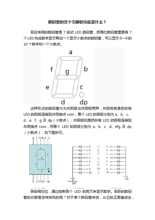
数码管的各个引脚的功能是什么?
现在常用的数码管是7段式LED数码管,即每位数码管里面有7个LED构成数字显示再加一个显示小数点的数码管,可以显示0—9的10个数字和一个小数点。
这种形式的数码管分为共阳极与共阴极两种,共阳极就是把所有LED的阳极连接到共同接点com,每个LED的阴极分别为a、b、c、d、e、f、g及dp(小数点);共阴极则是把所有LED的阴极连接到共同接点com,而每个LED的阳极分别为a、b、c、d、efg及dp (小数点),如下图所示。
各段相对应,通过控制各个LED的亮灭来显示数字。
实际的数码管的引脚是怎样排列的呢?对于单个数码管来说,从它的正面看进去,
左下角那个脚为1脚,以逆时针方向依次为1~10脚,左上角那个脚便是10脚了,上面图中的红色数字分别与这10个管脚一一对应。
注意,3脚和8脚是连通的,这两个都是公共脚。
还有一种比较常用的四位数码管,内部的四个数码管共用a~dp 8根数据线,因为里面有四个数码管,所以它还有四个位端,用来控制哪一位数字点亮,共有12个引脚,如上面图中,引脚排列依然是从左下角的那个脚(1脚)开始,以逆时针方向依次为1~12脚,与上图中的数字与之一一对应。
LED数码管及引脚图详细资料之欧阳理创编

LED数码管实际上是由七个发光管组成8字形构成的,加上小数点就是8个。
这些段分别由字母a,b,c,d,e,f,g,dp来表示。
当数码管特定的段加上电压后,这些特定的段就会发亮,以形成我们眼睛看到的2个8数码管字样了。
如:显示一个“2”字,那么应当是a亮b 亮g亮e亮d亮f不亮c不亮dp不亮。
LED数码管有一般亮和超亮等不同之分,也有0.5寸、1寸等不同的尺寸。
小尺寸数码管的显示笔画常用一个发光二极管组成,而大尺寸的数码管由二个或多个发光二极管组成,一般情况下,单个发光二极管的管压降为1.8V左右,电流不超过30mA。
发光二极管的阳极连接到一起连接到电源正极的称为共阳数码管,发光二极管的阴极连接到一起连接到电源负极的称为共阴数码管。
常用LED数码管显示的数字和字符是0、1、2、3、4、5、6、7、8、9、A、B、C、D、E、F。
led数码管(LED Segment Displays)是由多个发光二极管封装在一起组成“8”字型的器件,引线已在内部连接完成,只需引出它们的各个笔划,公共电极。
led数码管常用段数一般为7段有的另加一个小数点,还有一种是类似于3位“+1”型。
位数有半位,1,2,3,4,5,6,8,10位等等....,led数码管根据LED的接法不同分为共阴和共阳两类,了解LED的这些特性,对编程是很重要的,因为不同类型的数码管,除了它们的硬件电路有差异外,编程方法也是不同的。
图2是共阴和共阳极数码管的内部电路,它们的发光原理是一样的,只是它们的电源极性不同而已。
颜色有红,绿,蓝,黄等几种。
led 数码管广泛用于仪表,时钟,车站,家电等场合。
选用时要注意产品尺寸颜色,功耗,亮度,波长等。
下面将介绍常用LED数码管内部引脚图片10引脚的LED数码管图1 这是一个7段两位带小数点 10引脚的LED数码管LED数码管引脚定义图2 引脚定义每一笔划都是对应一个字母表示 DP是小数点.LED数码管要正常显示,就要用驱动电路来驱动数码管的各个段码,从而显示出我们要的数位,因此根据LED数码管的驱动方式的不同,可以分为静态式和动态式两类。
LED驱动控制专用电路-MR6928
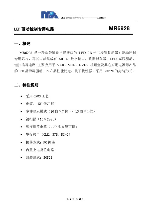
LED驱动控制专用电路MR6928━━━━━━━━━━━━━━━━━━━━━━━━━━━━━━━━━━━━━━━━━━━━━━━━━━━一、概述MR6928是一种款带键盘扫描接口的LED(发光二极管显示器)驱动控制专用芯片,再其内部集成有MCU、数字接口、数据锁存器、LED高压驱动、键扫描等电路,主要应用于VCR、VCD、DVD、机顶盒及其它家用电器等产品的LED显示屏驱动, 本产品性能稳定、抗干扰性强。
采用SOP28的封装形式。
二、特性说明∙采用CMOS工艺∙电源: 5V 低功耗∙多种显示模式(10段×7位~ 13段×4位)∙键扫描(10×2bit)∙辉度调节电路(占空比8级可调)∙串行接口(CLK,STB,DI/O)∙振荡方式:RC振荡∙内置上电复位电路∙封装形式:SOP28三、 内部功能框图:R四、 管脚定义:管脚功能定义:五、显示寄存器地址和显示模式:该寄存器存储通过串行接口从外部器件传送到MR6928的数据,地址分配如下:低4位高4位六、键扫描和键扫数据寄存器:键扫矩阵为10×2bit,如下所示:键扫数据储存地址如下所示,用读指令读取,读从低位开始:b0 ……b2 b3 ……b5 读取顺序七、 指令说明:指令用来设置显示模式和LED 驱动器的状态。
在STB 下降沿后由DI/O 输入的第一个字节作为一条指令。
如果在指令或数据传输时STB 被置为高电平,串行通讯被初始化,并且正在传送的指令或数据无效(之前传送的指令或数据保持有效)。
(1) 显示模式设置:该指令用来设置选择段和位的个数(4~7位,11~13段)。
当指令执行时,显示被强制终止,同时键扫描也停止。
要重新显示,显示开/关指令“ON ”必需被执行,但当相同模式被设置时,则上述情况并不发生。
上电时,设置模式为4位,13段。
(2) 数据设置: 该指令用来设置数据写和读(3) 地址设定:该指令用来设置显示寄存器的地址。
AIP1640 TM1640中微爱芯LED显示驱动芯片

产品说明书1、概述AiP1640 是一款2 线串口共阴极8 段16 位的LED 驱动控制专用电路,内部集成有MCU 数字接口、数据锁存器、LED 驱动等电路。
本产品性能优良,质量可靠。
其主要特点如下:内置显示RAM内置RC振荡内置自动消隐电路显示辉度软件可调两线串行接口(CLK,DATA)封装形式:SOP28/SSOP28(0.635mm)应用领域:LED显示面板场合,例如电磁炉显示、电饭煲显示、空调显示、电子秤等家电产品。
订购信息:管装:产品型号封装形式打印标识管装数盒装管盒装数箱装盒箱装数备注说明AiP1640SA.TB SOP28 AiP1640 25PCS/管80 管/盒2000PCS/盒10 盒/箱20000PCS/箱塑封体尺寸:17.9mm×7.5mm 引脚间距:1.27mmAiP1640VB.TB SSOP28 AiP1640 50PCS/管200 管/盒10000PCS/盒 5 盒/箱50000PCS/箱塑封体尺寸:9.9mm×3.9mm引脚间距0.635mm编带:产品型号封装形式打印标识编带盘装数编带盒装数箱装数备注说明塑封体尺寸:AiP1640SA.TR SOP28 AiP1640 1000PCS/盘1000PCS/盒8000PCS/箱17.9mm×7.5mm引脚间距:1.27mm 注:如实物与订购信息不一致,请以实物为准。
2、引脚图及引脚说明2.1、引脚排列图2.2、引脚说明引脚符号I/O 功能1 GRID12 O 位输出,N 管开漏输出2 GRID13 O 位输出,N 管开漏输出3 GRID14 O 位输出,N 管开漏输出4 GRID15 O 位输出,N 管开漏输出5 GRID16 O 位输出,N 管开漏输出6 GND —地7 DATA I 数据输入端口8 CLK I 时钟输入端口9 SEG1 O 段输出,P 管开漏输出10 SEG2 O 段输出,P 管开漏输出11 SEG3 O 段输出,P 管开漏输出12 SEG4 O 段输出,P 管开漏输出13 SEG5 O 段输出,P 管开漏输出14 SEG6 O 段输出,P 管开漏输出15 SEG7 O 段输出,P 管开漏输出16 SEG8 O 段输出,P 管开漏输出17 VDD —电源18 GRID1 O 位输出,N 管开漏输出19 GRID2 O 位输出,N 管开漏输出20 GRID3 O 位输出,N 管开漏输出21 GRID4 O 位输出,N 管开漏输出22 GRID5 O 位输出,N 管开漏输出23 GRID6 O 位输出,N 管开漏输出24 GRID7 O 位输出,N 管开漏输出25 GRID8 O 位输出,N 管开漏输出26 GRID9 O 位输出,N 管开漏输出27 GRID10 O 位输出,N 管开漏输出28 GRID11 O 位输出,N 管开漏输出3、电特性3.1、极限参数(除非有特殊说明,否则T amb=25℃,GND=0V)参数名称符号条件额定值单位电源电压VDD —-0.5~+7.0 V 逻辑输入电压VIN —-0.5~VDD+0.5 V 输出高电平电流(SEG)I O1 —50 mA 输出低电平电流(GRID)I O2 —200 mA 工作温度T amb —-40~+85 ℃储存温度T stg —-65~+150 ℃焊接温度T L 10 秒250 ℃3.2、推荐使用条件参数名称符号最小典型最大单位逻辑电源电压VDD 3 5 5.5 V 输入高电平电压V IH 0.7VDD —VDD V输入低电平电压V IL 0 —0.2VDD V3.3、电气特性3.3.1、直流参数(除非有特殊说明,否则VDD=5V,GND=0V)参数名称符号测试条件最小典型最大单位工作电压VDD — 3.0 5.0 5.5 V 静态电流I DD 无负载,VIN=VDD 110 130 150 uA 输出高电平电流I OH1 SEG1~SEG8,V OH=VDD-2V 40 50 60 mAI OH2 SEG1~SEG8,V OH=VDD-3V 40 60 80 mA 输出低电平电流I OL1 GRID1~GRID16,V OL= 0.3V 80 120 —mA 高电平输出电流容许量I TOLSG SEG1~SEG8,V OH=VDD-3V —— 5 %输入高电平电压V IH CLK、DATA 0.7VDD —VDD V输入低电平电压V IL CLK、DATA 0 —0.2VDD V3.3.2、交流参数(除非有特殊说明名,否则VDD=5V,GND=0V)参数符号测试条件最小典型最大单位振荡频率f OSC ——450 —kHz 上升时间t TZHC L=300pF,GRID1~GRID16 —— 2 usC L=300pF,SEG1~SEG8 ——0.5 us下降时间t THZ C L=300pF,SEGn、GRIDn ——120 us 最大时钟频率f max 占空比50% 1 ——MHz 时钟脉冲宽度PW CLK —400 ——ns 数据建立时间t SETUP —100 ——ns 数据保持时间t HOLD —100 ——ns4、功能介绍4.1、显示寄存器地址该寄存器存储通过串行接口从外部器件传送到AiP1640 的数据,地址分配如下:SEG1 SEG2 SEG3 SEG4 SEG5 SEG6 SEG7 SEG8B0 B1 B2 B3 B4 B5 B6 B7显存地址00H GRID1显存地址01H GRID2显存地址02H GRID3显存地址03H GRID4显存地址04H GRID5显存地址05H GRID6显存地址06H GRID7显存地址07H GRID8显存地址08H GRID9显存地址09H GRID10显存地址0AH GRID11显存地址0BH GRID12显存地址0CH GRID13显存地址0DH GRID14显存地址0EH GRID15显存地址0FH GRID16 注意:在上电完之后,必须先对RAM 进行数据写入,然后再开显示。
1 电路板各管脚及LED定义(例行试验大纲)
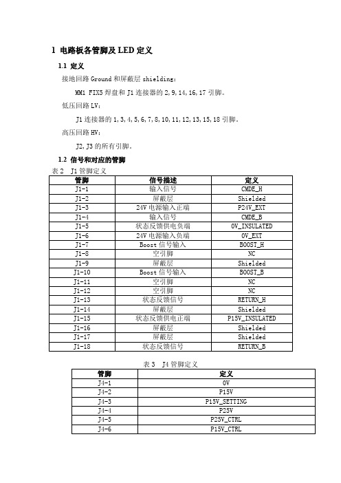
1.1 定义 接地回路 Ground 和屏蔽层 shielding: MM1 FIX5 焊盘和 J1 连接器的 2,9,14,16,17 引脚。 低压回路 LV: J1 连接器的 1,3,4,5,6,7,3 的所有引脚。 1.2 信号和对应的管脚 表2 J1 管脚定义 管脚 J1-1 J1-2 J1-3 J1-4 J1-5 J1-6 J1-7 J1-8 J1-9 J1-10 J1-11 J1-12 J1-13 J1-14 J1-15 J1-16 J1-17 J1-18 信号描述 输入信号 屏蔽层 24V 电源输入正端 输入信号 状态反馈供电负端 24V 电源输入负端 Boost 信号输入 空引脚 屏蔽层 Boost 信号输入 空引脚 空引脚 状态反馈信号 屏蔽层 状态反馈供电正端 屏蔽层 屏蔽层 状态反馈信号 表3 管脚 J4-1 J4-2 J4-3 J4-4 J4-5 J4-6 J4 管脚定义 定义 0V P15V P15V_SETTING P25V P25V_CTRL P15V_CTRL 定义 CMDE_H Shielded P24V_EXT CMDE_B 0V_INSULATED 0V_EXT BOOST_H NC Shielded BOOST_B NC NC RETURN_H Shielded P15V_INSULATED Shielded Shielded RETURN_B
J4-7 J4-8 J4-9 表4 管脚 J2-1 J2-2 J2-3 J2-4 J2-5 J2-6 管脚 J3-1 J3-2 J3-3 J3-4 J3-5 J3-6 管脚 LED1 LED2 LED3 J2 管脚定义
N12V_CTRL N12V 0V 定义 SUP_CTRL_ECR SUP _IGBT_EMITTER IGBT_ON 0V_FLOATING SUP _VCE_MEAS SUP_IGBT_GATE 表 5 J3 管脚定义 定义 INF_CTRL_ECR INF_IGBT_EMITTER IGBT_ON 0V_FLOATING INF_VCE_MEAS INF_IGBT_GATE 表 6 LED 定义 定义 红色,VCE 故障指示灯 黄色,开通信号指示灯 黄色,关断信号指示灯
数码管的各个引脚的功能是什么?
数码管的各个引脚的功能是什么?
现在常用的数码管是7段式LED数码管,即每位数码管里面有7个LED构成数字显示再加一个显示小数点的数码管,可以显示0—9的10个数字和一个小数点。
这种形式的数码管分为共阳极与共阴极两种,共阳极就是把所有LED的阳极连接到共同接点com,每个LED的阴极分别为a、b、c、d、e、f、g及dp(小数点);共阴极则是把所有LED的阴极连接到共同接点com,而每个LED的阳极分别为a、b、c、d、efg及dp (小数点),如下图所示。
各段相对应,通过控制各个LED的亮灭来显示数字。
实际的数码管的引脚是怎样排列的呢?对于单个数码管来说,从它的正面看进去,
左下角那个脚为1脚,以逆时针方向依次为1~10脚,左上角那个脚便是10脚了,上面图中的红色数字分别与这10个管脚一一对应。
注意,3脚和8脚是连通的,这两个都是公共脚。
还有一种比较常用的四位数码管,内部的四个数码管共用a~dp 8根数据线,因为里面有四个数码管,所以它还有四个位端,用来控制哪一位数字点亮,共有12个引脚,如上面图中,引脚排列依然是从左下角的那个脚(1脚)开始,以逆时针方向依次为1~12脚,与上图中的数字与之一一对应。
数码管驱动芯片TM1620『官方最新版』
矿产资源开发利用方案编写内容要求及审查大纲
矿产资源开发利用方案编写内容要求及《矿产资源开发利用方案》审查大纲一、概述
㈠矿区位置、隶属关系和企业性质。
如为改扩建矿山, 应说明矿山现状、
特点及存在的主要问题。
㈡编制依据
(1简述项目前期工作进展情况及与有关方面对项目的意向性协议情况。
(2 列出开发利用方案编制所依据的主要基础性资料的名称。
如经储量管理部门认定的矿区地质勘探报告、选矿试验报告、加工利用试验报告、工程地质初评资料、矿区水文资料和供水资料等。
对改、扩建矿山应有生产实际资料, 如矿山总平面现状图、矿床开拓系统图、采场现状图和主要采选设备清单等。
二、矿产品需求现状和预测
㈠该矿产在国内需求情况和市场供应情况
1、矿产品现状及加工利用趋向。
2、国内近、远期的需求量及主要销向预测。
㈡产品价格分析
1、国内矿产品价格现状。
2、矿产品价格稳定性及变化趋势。
三、矿产资源概况
㈠矿区总体概况
1、矿区总体规划情况。
2、矿区矿产资源概况。
3、该设计与矿区总体开发的关系。
㈡该设计项目的资源概况
1、矿床地质及构造特征。
2、矿床开采技术条件及水文地质条件。
RT5958-11-SP-CH-201611_brief
TD(OFF) CL[0:7]= 12pF
—
CDOUT= 12pF
Tf
—
11.4 61.8 20.7 5.32
—
— ns
—
—
Confidential Information
Page 5
建议应用电路
由于 LED扫瞄屏广泛应用于户内显示屏用以降低成本,但起因于 LED阳极的寄生电容于扫瞄切换时会 瞬间产生放电路径而造成显示屏发生残影现象; 用户可使用具有放电电路功能之 RT5958且参照如下 图的扫瞄屏建议应用电路,并搭配内建有预先充电功能的恒流IC (如 RT516S),如此即能够完整地消除 此上、下行残影现象。 由于 RT5958可以透过输入讯号设定内置换行扫描关断周期,故可以有效避免 LED灯芯遭反向电压击 穿,且于 LED发生开短路状况时不会产生串亮现象。 因 RT5958为 8路输出集成之电源芯片,为避免热积累过大,建议应使用于 16扫以上显示屏,并注意 实际使用时之热量状况。
[16扫及32扫串接图]
Confidential Information
Page 6
PCB布版设计注意事项
为求采用 RT5958行管芯片的灯版模块能够发挥高效能之显示效果且长期稳定地运作,除了模块本身 制作工艺及材料质量的要求提高外,PCB布版时电路组件放置规划及输入输出讯号走线设计等细节也是 必须讲究的; 针对灯版模块之 PCB布版设计应注意事项,以下将相关改善建议分成电源讯号稳定性、输入讯号噪声 干扰隔离及芯片245输出讯号等部分说明提供用户参考:
9 10 12
管脚名称 VDD DIN LCK BK
OUT[0:7]
GND DOUT
NC
描述 电源供应端(接1即可) 串行数据信号输入端 串行数据闪控 (data strobe) 信号输入端 電流输出使能信号端
LED显示屏IC脚位功能
LED显示屏IC脚位功能The role of 74HC245: signal power amplification.First feet DIR, for the input and output port conversion, DIR=, "1" high power signal by the "A" end input "B" side output, DIR= "0" low power signal by the "B" end input "A" end output.2~9 pin "A" signal input and output, A1=B1,,,,, and, A8=B8, A1 and B1 are a group, and if DIR= "1", "G=", "0", A1 enter B1 output, the other similar. If DIR= "0", "G=", "0", B1 enters the A1 output, which is similar.The 11~18 pin "B" signal input and output function is not the same as the "A" end.Nineteenth feet G, enabling the end, if the foot is "1", the A/B side of the signal will not be connected, only for "0" when the A/B terminal is enabled, the foot is played the role of the switch.Tenth feet GND, power ground.Twentieth feet VCC, power positive.The role of 74HC04: 6 bit inverter.Seventh feet GND, power ground.Fourteenth feet VCC, power positive.The signal is input from the A terminal, the Y end is invertingoutput, the A1 and the Y1 are one group, and the other is analogous. Example: A1= "1", Y1= "0", "A1=" "0", Y1= "1", and other group functions.The role of 74HC138: eight bit binary translation decimal decoder.Eighth feet GND, power ground.Fifteenth feet VCC, power positivePin 1~3, A, B, C, binary input pins.The 4~6 pin chip select signal control, only in 4, 5 feet to 0 feet 6 to 1, will be gated by A, B, C output signal control. Any other combination will not be selected, and the Y0~Y7 output will be "1"".Cascade through control gating to extend it to sixteen bits.Example: G2A=0, G2B=0, G1=1, A=1, B=0, C=0, Y0 is "0" and "Y1~Y7" is "1". See the truth table for details.The role of 74HC595: LED driver chip, 8 bit shift latch.Eighth feet GND, power ground.Sixteenth feet VCC, power positiveFourteenth feet DATA, serial data input, display data from this entry, must be accompanied by a clock signal in order to move.Thirteenth feet EN, enable the mouth, when the pin is "1", the QA~QH port is all "1", and when "0", the output of QA~QH is controlled by the input data.Twelfth feet STB, latch the mouth, when the input data in the incoming register, only the supply of a latch signal, in order to move data to the QA~QH port output.Eleventh feet CLK, the clock port, each clock signal will be moved to a data register.Tenth feet SCLR, reset port, as long as there is reset signal, the data moved in the register will be empty, the screen does not use this foot, generally connected to VCC.Ninth feet DOUT, serial data output, the data passed to the next.Fifteenth, 1~7 feet, parallel output port, that is, the driver output, driving LED.4953 function: line drive tube, power tube.The interior is two CMOS, 1, 2, 4 VCC 3 feet, 2 feet foot foot control, output control of 7, 8 feet, 4 feet, 6 feet 5 control output, only when the 2 foot, 4 to 0, 7, 8, 5, 6 will be output, otherwise the output is in the high impedance state.The role of TB62726: LED driver chip, 16 bit shift latch.First feet GND, power ground.Twenty-fourth feet VCC, power positiveSecond pin DATA, serial data inputThird feet CLK, clock inputFourth pin STB, latched inputTwenty-third pin output current adjustment end, resistance adjustmentTwenty-second pin DOUT, serial data outputTwenty-first feet EN, enable inputOther functions are similar to the 74HC595, except that the TB62726 is a 16 bit shift latch with an output current adjustment function, but there is no high level on the parallel output port, only the high impedance state and the low level state. The 74HC595 parallel output port has a high and low level output. The TB62726 is similar in structure to the 5026 pin function.Two, LED electronic display common signal understandingCLK clock signal: a shift pulse supplied to a shift register, each pulse causing data to be moved in or out of one bit. The data on the data port must be coordinated with the clock signal to transmit the data normally. The frequency of the data signalmust be 1/2 times of the clock signal. In any case, when the clock signal is abnormal, it will make the whole board display disorganized.STB latch signal: the data in the shift register is sent to the latch, and the data content is illuminated by the drive circuit to display the LED. But because the drive circuit is controlled by the EN enable signal, the premise of its lighting must be to make it open. The latch signal also needs to be coordinated with the clock signal to display the full image. In any case, when the latch signal is abnormal, it will cause the entire board to display confusion.EN enable signal: full screen brightness control signal, also used for screen blanking. As long as the duty cycle is adjusted, the brightness changes can be controlled. When the enable signal is abnormal, the whole screen will appear dim, dim or trailing.Data signal: the data needed to provide the display image. The data must be coordinated with the clock signal to transmit data to any display point. General in the display data signal RGB separated, if a data signal is shorted to positive or negative, then the corresponding color will appear bright or not bright, when the corresponding data signal is suspended when the color display is uncertain.ABCD signal: only exists in the dynamic scanning display, ABCD is actually a binary number, A is the lowest, if the binary representation of ABCD signal to control the maximum range is 16 (1111), 1/4 scan as long as the AB signal can be, becausethe AB signal range is 4 (11). When the control signal is abnormal, there will be a dislocation, highlight or image overlap phenomenon display.Three, common troubleshooting means (tools: multimeter, electric iron, blade, screwdriver, tweezers...... Et al.)The judgment problem must be dealt with first, second and second, and the obvious and serious first should be dealt with.Short circuit should be the highest priority.1, resistance detection method, the multimeter to detect a resistance profile, a normal circuit board to ground resistance value, and then detect the same point another piece of the same circuit board test and normal resistance values are different, if different from the scope of the problem.2, voltage detection method, the multimeter to voltage files,Detects the voltage of a point at a point in a suspected circuit, and compares whether it is similar to the normal value. Otherwise, the scope of the problem is determined.3, short circuit detection method, the multimeter toshort-circuit detection block (some files or file diode drop resistance, with alarm function), check whether there is a short-circuit phenomenon, found that after a short circuit should give priority to solving the problem, which does not burn other devices. The method must operate in the case of circuit failure and avoid damage to the meter.4, the pressure drop method, the multimeter to detect diode drop files, because all IC is composed of many single elements, only small, so when a pin it on a current is passed, will be on the pin voltage drop exists. In general, the same type of IC, the same pressure drop on the pin, according to the value of the pressure drop on the pin is good or bad, the circuit must be operated in the case of power failure. This method has some limitations, for example, when the detected device is high impedance, it can not be detected.Four 、 the method of unit board routing and the treatment of common problems1/16 unit board routing mode:1/8 unit board, 3 ways of routing:Static light plate wiring mode:* * this is only partial routing. To the unknown unit board, it is necessary to measure before the maintenance, to know its way of running, so as to facilitate the next step maintenance, so as to improve work efficiency.Board fault:A. the whole board is not bright1. Check whether the power supply is connected with the signal cable.2, check whether the test card to identify the interface test card is no red light flashing lamp plate recognition, check and test whether the components of power, or the lamp board interface signal and short circuit lead to the identification of interface. (intelligent test card)3, there is no weld detection of 74HC245 short circuit, 245 corresponding enable (EN) signal input and output pin whether weld or short circuit to the other line.Note: the main check power and enable (EN) signal.B. in the oblique scan, the regular line is not bright, the screen overlap1, A, B, C, check the D signal input port to 245 if there is a disconnection or short circuit,.2, detection of 245 corresponding A, B, C, D output and the 138 between the short-circuit or weld.3, detect A, B, C, D, whether the signal between the short circuit or a signal and ground short circuit.Note: ABCD line signal is detected mainly.When C. is full, one or more lines are not lit1, between 138 to 4953 of the detection circuit is short circuit or weld.When D. scans, two or more lines (usually multiples of 2, regular) are lit simultaneously1, detect A, B, C, D, whether the signal between the short circuit.2. Check whether the 4953 output terminal is shorted to other output terminals.E. full light with one or more dots (irregular) not bright1. Find the control pin corresponding to this module and measure if it is shorted to the bank.2. Replace module or single light.When F. is full, one or more columns are not lit1. Find the pin that controls the column on the module and measure whether it is connected with the drive IC(74HC595/TB62726, -) output terminal.G. has single or single column highlighting, or full line highlighting, and is not controlled1. Check whether the column is short circuited with the power source.2. Check whether the line is short circuited with the power supply.3, replace its drive IC.The H. displays confusion, but the output to the next board is normal1. Check whether the 245 STB latch outputs are connected to the latch end of the drive IC or the signal is shorted to another line.I. displays confusion and output is abnormal1, detect clock CLK latch, STB signal is short circuit.2, detect 245 clock CLK whether there is input or output.3, check whether the clock signal is short circuited to other lines.Note: the clock and latch signal are mainly detected.J. shows lack of color1, detect 245 of the color of the data terminal whether there is input or output.2. Check whether the data signal of this color is short circuited to another line.3, the color detection between driving IC cascade data port is open circuit or short circuit,.Note: the voltage detection method can be used to find the problem more easily, and the voltage of the data port is different from the normal one, so that the fault area can be determined.There is a problem with the K. output1 、 check the output interface to the signal output IC whether the line is connected or shorted.2, detect the output clock latch signal is normal.3. Check whether the output of the last drive IC is connected with the data port of the output interface or whether it is short circuited.4 whether the output signals are short circuited or shorted to the ground.5, check the output cable is good.Whole screen fault:A. the whole screen is not bright (Hei Ping)1. Check whether the power supply is powered on.2 、 check whether the communication line is connected or not. (Tong Buping)3 、 the synchronous screen detects whether the sending card and the receiving card communicate with the green light or not.4. Whether the computer monitor is protected or the display area is black or pure blue. (Tong Buping)B. the whole panel is not bright (Hei Ping)1, a few pieces of plate transverse direction is not bright, check the normal unit plate and abnormal unit plate between the cable connection is connected; or chip 245 is normal,2, several continuous plate longitudinal direction is not bright, check the power supply of this column is normal.The C. board is not up1, check the line and the 4953 output foot is.2, check whether 138 normal.3 check whether the 4953 burns or burns.4, check whether there is a high level 4953.5. Check whether the 138 and 4953 control pins are connected.The D. unit board is not lit1, check whether 595 normal.2. Check whether the upper and lower modules are connected.3, check the 595 output pin to the foot of the module is connected. The E. module loses color 1 and checks whether the 245 R.G data has output.2, check the normal 595 output pin and the abnormal 595 input pins are connected.。
- 1、下载文档前请自行甄别文档内容的完整性,平台不提供额外的编辑、内容补充、找答案等附加服务。
- 2、"仅部分预览"的文档,不可在线预览部分如存在完整性等问题,可反馈申请退款(可完整预览的文档不适用该条件!)。
- 3、如文档侵犯您的权益,请联系客服反馈,我们会尽快为您处理(人工客服工作时间:9:00-18:30)。
一、1.2 LED板的芯片功能74HC245的作用:信号功率放大。
第1脚DIR,为输入输出转换端口,当DIR=“1”高电平(接VCC)时信号由“A”端输入“B”端输出,DIR=“0”低电平(接GND)时信号由“B”端输入“A”端输出。
第19脚G,使能端,若该脚为“1”A/B端的信号将不导通,只有为“0”时A/B 端才被启用,该脚也就是起到开关的作用.第2~9脚“A”信号输入\输出端,A1=B1、、、、、、A8=B8,A1与B1是一组,如果DIR=“1”G=“0”则A1输入B1输出,其它类同。
如果DIR=“0”G=“0”则B1输入A1输出,其它类同。
第11~18脚“B”信号输入\输出端,功能与“A”端一样。
第10脚GND,电源地。
第20脚VCC,电源正极。
74HC595的作用:LED驱动芯片,8位移位锁存器。
第8脚GND,电源地。
第16脚VCC,电源正极第14脚DATA,串行数据输入口,显示数据由此进入,必须有时钟信号的配合才能移入。
QA~QH的输出由输入的数据控制。
第12脚STB,锁存端,当输入的数据在传入寄存器后,只有供给一个锁存信号才能将移入的数据送QA~QH口输出。
第11脚CLK,时钟端,每一个时钟信号将移入一位数据到寄存器。
第10脚SCLR,复位端,只要有复位信号,寄存器内移入的数据将清空,显示屏不用该脚,一般接VCC。
第9脚DOUT,串行数据输出端,将数据传到下一个。
第15、1~7脚,并行输出端也就是驱动输出端,驱动LED。
HC16126\TB62726的作用:LED驱动芯片,16位移位锁存器。
备注:HC16126驱动芯片定义和5020,5024,2016等芯片一样第1脚GND,电源地。
第24脚VCC,电源正极第2脚DATA,串行数据输入第3脚CLK,时钟输入第4脚STB,锁存输入第23脚输出电流调整端,接电阻调整第22脚DOUT,串行数据输出第21脚EN,使能输入其它功能与74HC595相似,只是TB62726是16位移位锁存器,并带输出电流调整功能,但在并行输出口上不会出现高电平,只有高阻状态和低电平状态。
74HC595并行输出口有高电平和低电平输出。
TB62726与5026的引脚功能一样,结构相似。
74HC138的作用:八位二进制译十进制译码器。
第8脚GND,电源地。
第16脚VCC,电源正极第1~3脚A、B、C,二进制输入端。
第4~6脚片选信号控制,只有在第4、5脚为“0”第6脚为“1”时,才会被选通,输出受A、B、C信号控制。
其它任何组合方式将不被选通,且Y0~Y7输出全为“1”。
通过控制选通脚来级联,使之扩展到十六位。
例:G2A=0,G2B=0,G1=1,A=1,B=0,C=0,则Y0为“0”Y1~Y7为“1”,4953的作用:行驱动管,功率管。
其内部是两个CMOS管,1、3脚VCC,2、4脚控制脚,2脚控制7、8脚的输出,4脚控制5、6脚的输出,只有当2、4脚为“0”时,7、8、5、6才会输出,否则输出为高阻状态.74HC04的作用:6位反相器。
第7脚GND,电源地。
第14脚VCC,电源正极。
信号由A端输入Y端反相输出,A1与Y1为一组,其它类推。
例:A1=“1”则Y1=“0”、A1=“0”则Y1=“1”,2、常见信号的了解2.1 CLK时钟信号:提供给移位寄存器的移位脉冲,每一个脉冲将引起数据移入或移出一位。
数据口上的数据必须与时钟信号协调才能正常传送数据,数据信号的频率必须是时钟信号的频率的1/2倍。
在任何情况下,当时钟信号有异常时,会使整板显示杂乱无章。
2.2 STB锁存信号:将移位寄存器内的数据送到锁存器,并将其数据内容通过驱动电路点亮LED显示出来。
但由于驱动电路受EN使能信号控制,其点亮的前提必须是使能为开启状态。
锁存信号也须要与时钟信号协调才能显示出完整的图象。
在任何情况下,当锁存信号有异常时,会使整板显示杂乱无章。
2.3 EN使能信号:整屏亮度控制信号,也用于显示屏消隐。
只要调整它的占空比就可以控制亮度的变化。
当使能信号出现异常时,整屏将会出现不亮、暗亮或拖尾3、EN使能信号等现象。
2.4 数据信号:提供显示图象所需要的数据。
必须与时钟信号协调才能将数据传送到任何一个显示点。
一般在显示屏中红绿蓝的数据信号分离开来,若某数据信号短路到正极或负极时,则对应的该颜色将会出现全亮或不亮,当数据信号被悬空时对应的颜色显示情况不定。
2.5 ABCD行信号:只有在动态扫描显示时才存在,ABCD是二进制数,A 是最低位,D是最高位,如果用二进制表示ABCD信号控制最大范围是16行(1111),1/4扫描中只要AB信号就可以了,因为AB信号的表示范围是4行(11)。
当行控制信号出现异常时,将会出现显示错位、高亮或图像重叠等现象。
1、常见故障处理方式:1.1、电阻检测法:将万用表调到电阻档,检测一块正常的电路板的某点的到地电阻值,再检测另一块相同的电路板的同一个点测试与正常的电阻值是否有不同,若不同则就确定了问题的范围。
1.2、电压检测法:将万用表调到电压档,检测怀疑有问题的电路的某个点的到地电压,比较是否与正常值相似,否则确定了问题的范围。
1.3、短路检测法:将万用表调到短路检测挡(有的是二极管压降档或是电阻档,一般具有报警功能),检测是否有短路的现象出现,发现短路后应优先解决,使之不烧坏其它器件。
该法必须在电路断电的情况下操作,避免损坏表。
1.4、压降检测法:将万用表调到二极管压降检测档,因为所有的IC都是由基本的众多单元件组成,只是小型化了,所以在当它的某引脚上有电流通过时,就会在引脚上存在电压降。
2、单元板走线方式与常见问题的处理步骤2.1 整板故障A.整板不亮1、检查供电电源与信号线是否连接。
2、检测74HC245有无虚焊短路,245上对应的使能(EN)信号输入输出脚是否虚焊或短路到其它线路。
注:主要检查电源与使能(EN)信号。
B.在点斜扫描时,规律性的隔行不亮显示画面重叠。
1、检查A、B、C、D信号输入口到245之间是否有断线或虚焊、短路。
2、检测245对应的A、B、C、D输出端与138之间是否断路或虚焊、短路。
3、检测A、B、C、D各信号之间是否短路或某信号与地短路。
注:主要检测ABCD行信号。
C.全亮时有一行或几行不亮1、检测138到4953之间的线路是否断路或虚焊、短路。
2、检测4953到H之间的线路是否断路或虚焊、短路。
D.显示混乱,输出不正常1、检测时钟CLK锁存STB信号是否短路。
2、检测245的时钟CLK是否有输入输出。
3、检测时钟信号是否短路到其它线路。
注:主要检测时钟与锁存信号。
E.全亮时有单点或多点(无规律的)不亮1、找到该模块对应的控制脚测量是否与本行短路。
2、更换模块或单灯。
F.全亮时有一列或几列不亮1、在模块上找到控制该列的引脚,测是否与驱动IC(74HC595/TB62726、、、)输出端连接。
G.有单点或单列高亮,或整行高亮,并且不受控1、检查该列是否与电源地短路。
2、检测该行是否与电源正极短路。
3、更换其驱动IC。
H.显示混乱,但输出到下一块板的信号正常1、检测245对应的STB锁存输出端与驱动IC的锁存端是否连接或信号被短路到其它线路。
I.显示混乱,输出不正常1、检测时钟CLK锁存STB信号是否短路。
2、检测245的时钟CLK是否有输入输出。
3、检测时钟信号是否短路到其它线路。
注:主要检测时钟与锁存信号。
J.显示缺色1、检测245的该颜色的数据端是否有输入输出。
2、检测该颜色的数据信号是否短路到其它线路。
3、检测该颜色的驱动IC之间的级连数据口是否有断路或短路、虚焊。
注:可使用电压检测法较容易找到问题,检测数据口的电压与正常的是否不同,确定故障区域。
K.输出有问题1、检测输出接口到信号输出IC的线路是否连接或短路。
2、检测输出口的时钟锁存信号是否正常。
3、检测最后一个驱动IC之间的级连输出数据口是否与输出接口的数据口连接或是否短路。
4、输出的信号是否有相互短路的或有短路到地的。
5、检查输出的排线是否良好。
2.2 故障现象1 单元板出现一条行长亮、暗亮、不亮。
检查维修:(1)目测单元板上的行管引出脚是否虚焊;如果是,将引脚焊好。
(2)用万用表测量行管输出端是否和模块脚有通,如没通:用数据线连上,如有通,再测是否和地短路,如无,测电压是否正常(万用表测量方法:黑表笔接GND、红表笔去测量各个管脚的电压);如是,则判断行输出端与所对应的模块管脚断路;如否,测量行管的输入端是否正常;如是,则行管坏、用同型号行管换之;如否,测量所对应HC138的输出端是否正常;如是,则判断HC138的输出端与行管的输入端断路;若否,则判断HC138H坏。
(3)如果以上测量均属正常,则行管本身存在质量问题,用同型号行管换之。
2 单元板出现一列长亮、暗亮、不亮。
检查维修:(1)目测单元板上故障所对应的模块管脚及集成电路是否虚焊、短路、断路;如是,将引脚焊好。
(2)用万用表测量HC595的输出端【HC595的输出引脚:1、2、3、4、5、6、7、15共八列控制端;测量时应区分红、绿集成电路、顺序排列为:红、绿(R、G)】电压是否正常;如是,则判断HC595输出端与模块输入端断路;如否,则判断HC595坏、用同型号的HC595集成电路换之(替换集成电路HC595时,注意电路引线别断开)。
如HC595都正常那判断模块坏用同一型号的模块换上3 单元板出现八点行、列或单点不亮、长亮、暗亮及16点。
检查维修:(1)目测故障所对应的模块引脚及引线有无短路、虚焊、断路。
(2)每小区(单元板共分上下两小区)的上下、左右模块之间共用连接线是否正常(将万用表置与相邻端,测量模块行输入端及各个控制输入端的引线连接),若是,则判断为模块坏,如否,可直接用细数据线代替接通即可消除。
(3)可用万用表直接测量单个模块是否正常,如是,则判断为电路板与模块间的内部短路,如否则判断为模块坏,用同型号模块替换。
4 单元板出现几行或整小区(单元板共分上下两小区)不亮、长亮、暗亮。
检查维修:(1)目测所对应的行管、穿心电感、集成电路是否虚焊、短路、断路,如是,将短路处断开及虚焊、断路处重新焊好。
(2)用万用表测量各个行管输出端电压是否正常(万用表测量方法:黑表笔接GND、红表笔去测量各个管脚的电压);如是,则判断行输出端与所对应的模块管脚断路;如否,测量行管的输入端是否正常;如是,则行管坏、用同型号行管换之;如否,测量所对应HC138的输出端是否正常;如是,则判断HC138的输出端与行管的输入端断路;如否,则判断HC138坏。
(3)用好的16P排线替换试一下,测量HC138地址输入端1、2、3引脚电压、选通端4、5(低电平有效)、6(高电平有效)及集成电路供电是否正常,如是,则判断为HC138坏,再则以(2)续查。