An optically driven quantum dot quantum computer
EndNote Papers

Adinolfi, V., et al. (2015). "Photojunction Field-Effect Transistor Based on a Colloidal Quantum Dot Absorber Channel Layer." ACS Nano 9(1): 356-362.Benayas, A., et al. (2015). "PbS/CdS/ZnS Quantum Dots: A Multifunctional Platform for In Vivo Near-Infrared Low-Dose Fluorescence Imaging." Advanced Functional Materials 25(42): 6650-6659.Carey, G. H., et al. (2015). "Record Charge Carrier Diffusion Length in Colloidal Quantum Dot Solids via MutualDot-To-Dot Surface Passivation." Advanced Materials 27(21): 3325-3330.Chen, H. Y., et al. (2016). "Nanostructured Photodetectors: From Ultraviolet to Terahertz." Advanced Materials 28(3): 403-433.Cheng, H. C., et al. (2016). "van der Waals Heterojunction Devices Based on Organohalide Perovskites andTwo-Dimensional Materials." Nano Letters 16(1): 367-373.Dang, V. Q., et al. (2015). "Ultrahigh Responsivity in Graphene-ZnO Nanorod Hybrid UV Photodetector." Small 11(25): 3054-3065.de Arquer, F. P. G., et al. (2015). "Tailoring the Electronic Properties of Colloidal Quantum Dots inMetal-Semiconductor Nanocomposites for High Performance Photodetectors." Small 11(22): 2636-2641.Deng, H., et al. (2015). "Flexible and Semitransparent Organolead Triiodide Perovskite Network Photodetector Arrays with High Stability." Nano Letters 15(12): 7963-7969.Deng, W., et al. (2016). "Aligned Single-Crystalline Perovskite Microwire Arrays for High-Performance Flexible Image Sensors with Long-Term Stability." Advanced Materials 28(11): 2201-2208.Domanski, K., et al. (2015). "Working Principles of Perovskite Photodetectors: Analyzing the Interplay Between Photoconductivity and Voltage-Driven Energy-Level Alignment." Advanced Functional Materials 25(44): 6936-6947.Dong, R., et al. (2015). "High-Gain and Low-Driving-Voltage Photodetectors Based on Organolead Triiodide Perovskites." Advanced Materials 27(11): 1912-+.Dou, L., et al. (2014). "Solution-processed hybrid perovskite photodetectors with high detectivity." Nature Communications 5.Photodetectors capture optical signals with a wide range of incident photon flux density and convert them to electrical signals instantaneously. They have many important applications including imaging, opticalcommunication, remote control, chemical/biological sensing and so on. Currently, GaN, Si and InGaAsphotodetectors are used in commercially available products. Here we demonstrate a novelsolution-processed photodetector based on an organic–inorganic hybrid perovskite material. Operating at room temperature, the photodetectors exhibit a large detectivity (the ability to detect weak signals)approaching 1014 Jones, a linear dynamic range over 100 decibels (dB) and a fast photoresponse with 3-dB bandwidth up to 3 MHz. The performance is significantly better than most of the organic, quantum dot and hybrid photodetectors reported so far; and is comparable, or even better than, the traditional inorganicsemiconductor-based photodetectors. Our results indicate that with proper device interface design,perovskite materials are promising candidates for low-cost, high-performance photodetectors.Erhard, N., et al. (2015). "Ultrafast Photodetection in the Quantum Wells of Single AlGaAs/GaAs-Based Nanowires." Nano Letters 15(10): 6869-6874.Fang, Y. J., et al. (2015). "Highly narrowband perovskite single-crystal photodetectors enabled by surface-charge recombination." Nature Photonics 9(10): 679-+.Gao, J. B., et al. (2015). "Carrier multiplication detected through transient photocurrent in device-grade films of leadselenide quantum dots." Nature Communications 6.Gao, L., et al. (2016). "Broadband, sensitive and spectrally distinctive SnS2 nanosheet/PbS colloidal quantum dot hybrid photodetector." Light Sci Appl. 5: e16126.Photodetectors convert photons into current or voltage outputs and are thus widely used for spectroscopy, imaging and sensing. Traditional photodetectors generally show a consistent-polarity response to incident photons within their broadband responsive spectrum. Here we introduced a new type of photodetectoremploying SnS2 nanosheets sensitized with PbS colloidal quantum dots (CQDs) that are not only sensitive(~105[thinsp]A[thinsp]W-1) and broadband (300-1000[thinsp]nm) but also spectrally distinctive, that is, show distinctive (positive or negative) photoresponse toward incident photons of different wavelengths. A careful mechanism study revealed illumination-modulated Schottky contacts between SnS2 nanosheets and Auelectrodes, altering the photoresponse polarity toward incident photons of different wavelengths. Finally, we applied our SnS2 nanosheet/PbS CQDs hybrid photodetector to differentiate the color temperature ofemission from a series of white light-emitting diodes (LEDs), showcasing the unique application of our novel photodetectors.Giansante, C., et al. (2015). ""Darker-than-Black" PbS Quantum Dots: Enhancing Optical Absorption of Colloidal Semiconductor Nanocrystals via Short Conjugated Ligands." Journal of the American Chemical Society 137(5):1875-1886.Guzman, A., et al. (2015). "Role of the wetting layer in the enhanced responsivity of InAs/GaAsSb quantum dot infrared photodetectors." Applied Physics Letters 107(1).Haider, G., et al. (2016). "Electrical-Polarization-Induced Ultrahigh Responsivity Photodetectors Based on Graphene and Graphene Quantum Dots." Advanced Functional Materials 26(4): 620-628.Hu, F. R., et al. (2015). "Superior Optical Properties of Perovskite Nanocrystals as Single Photon Emitters." ACS Nano 9(12): 12410-12416.Huang, Y., et al. (2016). "Highly sensitive photodetectors based on hybrid 2D-0D SnS2-copper indium sulfide quantum dots." Applied Physics Letters 108(1).Jang, D. M., et al. (2015). "Reversible Halide Exchange Reaction of Organometal Trihalide Perovskite Colloidal Nanocrystals for Full-Range Band Gap Tuning." Nano Letters 15(8): 5191-5199.Jang, S., et al. (2015). "Multifunctional Graphene Optoelectronic Devices Capable of Detecting and Storing Photonic Signals." Nano Letters 15(4): 2542-2547.Jansen-van Vuuren, R. D., et al. (2016). "Organic Photodiodes: The Future of Full Color Detection and Image Sensing." Advanced Materials 28(24): 4766-4802.Jiang, Z. Y., et al. (2015). "Suppression of dark current through barrier engineer for solution-processed colloidal quantum-dots infrared photodetectors." Applied Physics Letters 107(9).Jin, Z. W., et al. (2016). "Graphdiyne:ZnO Nanocomposites for High-Performance UV Photodetectors." Advanced Materials 28(19): 3697-3702.Johnston, M. B. (2015). "Colour-selective photodiodes." Nature Photonics 9(10): 633-636.Kagan, C. R. and C. B. Murray (2015). "Charge transport in strongly coupled quantum dot solids." Nature Nanotechnology 10(12): 1013-1026.Kufer, D. and G. Konstantatos (2015). "Highly Sensitive, Encapsulated MoS2 Photodetector with Gate Controllable Gain and Speed." Nano Letters 15(11): 7307-7313.Kufer, D., et al. (2015). "Hybrid 2D-0D MoS2-PbS Quantum Dot Photodetectors." Advanced Materials 27(1): 176-180. Lee, J. W., et al. (2016). "Inorganic UV-Visible-SWIR Broadband Photodetector Based on Monodisperse PbS Nanocrystals." Small 12(10): 1328-1333.Lee, J. W., et al. (2015). "Unraveling the Gain Mechanism in High Performance Solution-Processed PbS Infrared PIN Photodiodes." Advanced Functional Materials 25(8): 1233-1238.Lee, Y., et al. (2015). "High-Performance Perovskite-Graphene Hybrid Photodetector." Advanced Materials 27(1):41-46.Lhuillier, E., et al. (2015). "Nanoplatelets Bridging a Nanotrench: A New Architecture for Photodetectors with Increased Sensitivity." Nano Letters 15(3): 1736-1742.Lhuillier, E., et al. (2016). "Infrared Photodetection Based on Colloidal Quantum-Dot Films with High Mobility and Optical Absorption up to THz." Nano Letters 16(2): 1282-1286.Li, F., et al. (2015). "Ambipolar solution-processed hybrid perovskite phototransistors." Nature Communications 6. Lin, Q. Q., et al. (2015). "Filterless narrowband visible photodetectors." Nature Photonics 9(10): 687-+.Lin, Q. Q., et al. (2015). "Low Noise, IR-Blind Organohalide Perovskite Photodiodes for Visible Light Detection and Imaging." Advanced Materials 27(12): 2060-2064.Liu, J. Y., et al. (2016). "Two-Dimensional CH(3)NH(3)Pbl(3) Perovskite: Synthesis and Optoelectronic Application." ACS Nano 10(3): 3536-3542.Liu, X. J., et al. (2016). "Photoinduced surface voltage mapping study for large perovskite single crystals." Applied Physics Letters 108(18).Liu, Y., et al. (2016). "Room Temperature Broadband Infrared Carbon Nanotube Photodetector with High Detectivity and Stability." Advanced Optical Materials 4(2): 238-245.Long, M. S., et al. (2016). "Broadband Photovoltaic Detectors Based on an Atomically Thin Heterostructure." Nano Letters 16(4): 2254-2259.Lu, H., et al. (2016). "A Self-Powered and Stable All-Perovskite Photodetector-Solar Cell Nanosystem." Advanced Functional Materials 26(8): 1296-1302.Nikitskiy, I., et al. (2016). "Integrating an electrically active colloidal quantum dot photodiode with a graphene phototransistor." Nature Communications 7.Pan, L. L., et al. (2015). "Truly Fluorescent Excitation-Dependent Carbon Dots and Their Applications in Multicolor Cellular Imaging and Multidimensional Sensing." Advanced Materials 27(47): 7782-7787.Park, S., et al. (2015). "Significant Enhancement of Infrared Photodetector Sensitivity Using a Semiconducting Single-Walled Carbon Nanotube/C-60 Phototransistor." Advanced Materials 27(4): 759-765.Ramiro, I., et al. (2015). "Optically Triggered Infrared Photodetector." Nano Letters 15(1): 224-228.Ray, N., et al. (2015). "Measuring Ligand-Dependent Transport in Nanopatterned PbS Colloidal Quantum Dot Arrays Using Charge Sensing." Nano Letters 15(7): 4401-4405.Rim, Y. S., et al. (2016). "Recent Progress in Materials and Devices toward Printable and Flexible Sensors." Advanced Materials 28(22): 4415-4440.Rim, Y. S., et al. (2015). "Ultrahigh and Broad Spectral Photodetectivity of an Organic-Inorganic Hybrid Phototransistor for Flexible Electronics." Advanced Materials 27(43): 6885-+.Saidaminov, M. I., et al. (2015). "Planar-integrated single-crystalline perovskite photodetectors." Nature Communications 6.Saidaminov, M. I., et al. (2015). "Planar-integrated single-crystalline perovskite photodetectors." Nature Communications 6.Hybrid perovskites are promising semiconductors for optoelectronic applications. However, they suffer from morphological disorder that limits their optoelectronic properties and, ultimately, device performance.Recently, perovskite single crystals have been shown to overcome this problem and exhibit impressiveimprovements: low trap density, low intrinsic carrier concentration, high mobility, and long diffusion length that outperform perovskite-based thin films. These characteristics make the material ideal for realizingphotodetection that is simultaneously fast and sensitive; unfortunately, these macroscopic single crystalscannot be grown on a planar substrate, curtailing their potential for optoelectronic integration. Here weproduce large-area planar-integrated films made up of large perovskite single crystals. These crystalline films exhibit mobility and diffusion length comparable with those of single crystals. Using this technique, weproduced a high-performance light detector showing high gain (above 104 electrons per photon) and high gain-bandwidth product (above 108[thinsp]Hz) relative to other perovskite-based optical sensors.Saidaminov, M. I., et al. (2016). "Perovskite Photodetectors Operating in Both Narrowband and Broadband Regimes." Advanced Materials: n/a-n/a.Saran, R. and R. J. Curry (2016). "Lead sulphide nanocrystal photodetector technologies." Nature Photonics 10(2):81-92.Shao, D. L., et al. (2015). "Organic-Inorganic Heterointerfaces for Ultrasensitive Detection of Ultraviolet Light." Nano Letters 15(6): 3787-3792.Shen, L., et al. (2016). "A Highly Sensitive Narrowband Nanocomposite Photodetector with Gain." Advanced Materials 28(10): 2043-+.Shin, D. H., et al. (2015). "Graphene/Si-Quantum-Dot Heterojunction Diodes Showing High Photosensitivity Compatible with Quantum Confinement Effect." Advanced Materials 27(16): 2614-2620.Spina, M., et al. (2015). "Microengineered CH3NH3PbI3 Nanowire/Graphene Phototransistor for Low-Intensity Light Detection at Room Temperature." Small 11(37): 4824-4828.Su, L., et al. (2015). "High-Performance Organolead Halide Perovskite-Based Self-Powered Triboelectric Photodetector." ACS Nano 9(11): 11310-11316.Sutherland, B. R., et al. (2015). "Sensitive, Fast, and Stable Perovskite Photodetectors Exploiting Interface Engineering." ACS Photonics 2(8): 1117-1123.Trung, T. Q., et al. (2015). "Infrared Detection Using Transparent and Flexible Field-Effect Transistor Array with Solution Processable Nanocomposite Channel of Reduced Graphene Oxide and P(VDF-TrFE)." Advanced Functional Materials 25(11): 1745-1754.Wang, F. J., et al. (2016). "Temperature independent infrared responsivity of a quantum dot quantum cascade photodetector." Applied Physics Letters 108(25).Wang, L., et al. (2015). "Plasmon-Enhanced Fluorescence-Based Core-Shell Gold Nanorods as a Near-IR Fluorescent Turn-On Sensor for the Highly Sensitive Detection of Pyrophosphate in Aqueous Solution." Advanced Functional Materials 25(45): 7017-7027.Wang, W. Z., et al. (2016). "Visible blind ultraviolet photodetector based on CH3NH3PbCl3 thin film." Optics Express 24(8): 8411-8419.Wang, Y. S., et al. (2015). "Hybrid Graphene-Perovskite Phototransistors with Ultrahigh Responsivity and Gain." Advanced Optical Materials 3(10): 1389-1396.Wang, Z. N., et al. (2015). "Light-induced pyroelectric effect as an effective approach for ultrafast ultraviolet nanosensing." Nature Communications 6.Wei, H. T., et al. (2016). "Sensitive X-ray detectors made of methylammonium lead tribromide perovskite single crystals." Nature Photonics 10(5): 333-+.Wei, H. T., et al. (2015). "Trap Engineering of CdTe Nanoparticle for High Gain, Fast Response, and Low NoiseP3HT:CdTe Nanocomposite Photodetectors." Advanced Materials 27(34): 4975-+.Wu, J., et al. (2016). "Monolithically Integrated InAs/GaAs Quantum Dot Mid-Infrared Photodetectors on Silicon Substrates." ACS Photonics 3(5): 749-753.Xu, J. X., et al. (2015). "Atomic layer deposition of absorbing thin films on nanostructured electrodes forshort-wavelength infrared photosensing." Applied Physics Letters 107(15).Xu, Z. J., et al. (2016). "Monolayer MoS2/GaAs heterostructure self-driven photodetector with extremely high detectivity." Nano Energy 23: 89-96.Yakunin, S., et al. (2015). "Detection of X-ray photons by solution-processed lead halide perovskites." Nature Photonics 9(7): 444-U444.Yu, T., et al. (2016). "Graphene Coupled with Silicon Quantum Dots for High-Performance Bulk-Silicon-Based Schottky-Junction Photodetectors." Advanced Materials 28(24): 4912-4919.Zhang, L. Z., et al. (2015). "Toward Highly Sensitive Polymer Photodetectors by Molecular Engineering." Advanced Materials 27(41): 6496-+.Zhang, Q., et al. (2015). "Solution-Processed Graphene Quantum Dot Deep-UV Photodetectors." ACS Nano 9(2): 1561-1570.Zhang, Y. J., et al. (2016). "Ultrasensitive photodetectors exploiting electrostatic trapping and percolation transport." Nature Communications 7.Zhu, P. C., et al. (2016). "Direct Conversion of Perovskite Thin Films into Nanowires with Kinetic Control for Flexible Optoelectronic Devices." Nano Letters 16(2): 871-876.Zhu, Z. A., et al. (2016). "Excitonic Resonant Emission-Absorption of Surface Plasmons in Transition Metal Dichalcogenides for Chip-Level Electronic-Photonic Integrated Circuits." ACS Photonics 3(5): 869-874.。
OCDMA系统简介及应用
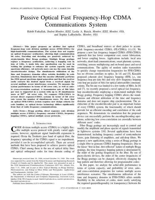
Passive Optical Fast Frequency-Hop CDMA Communications SystemHabib Fathallah,Student Member,IEEE,Leslie A.Rusch,Member,IEEE,Member,OSA,and Sophie LaRochelle,Member,OSAAbstract—This paper proposes an all-fiber fast optical frequency-hop code division multiple access(FFH-CDMA)for high-bandwidth communications.The system does not require an optical frequency synthesizer,allowing high communication bit rates.Encoding and decoding are passively achieved by strain-tunablefiber Bragg gratings.Multiple Bragg gratings replace a frequency synthesizer,achieving a hopping rate in tens of GHz.A main lobe sinc apodization can be used in writing the gratings to enhance the system capacity and the spectrum efficiency.All network users can use the same tunable encoder/decoder design.The simultaneous utilization of the time and frequency domains offers notableflexibility in code selection.Simulations show that the encoder efficiently performs the FFH spread spectrum signal generation and that the receiver easily extracts the desired signal from a received signal for several multiple access interference scenarios.We measure the system performance in terms of bit error rate,as well as auto-to cross-correlation contrast.A transmission rate of500Mb/s per user is supported in a system with up to30simultaneous users at1009bit error rate.We compare FFH-CDMA to several direct sequence-CDMA systems in terms of bit error rate versus the number of simultaneous users.We show that an optical FFH-CDMA system requires new design criteria for code families,as optical device technology differs significantly from that of radio frequency communications.Index Terms—Bragg grating,direct sequence code division multiple access(CDMA);frequency encoded CDMA,frequency hopping CDMA,optical multiple access protocols.I.I NTRODUCTIONC ODE division multiple access(CDMA)is a highlyflex-ible multiple access protocol with greatly varied appli-cations,however,significant signal bandwidth expansion is required.Given the Terahertz pass band of opticalfiber,the frequency spreading of the CDMA signal is no impediment, provided it can be accomplished optically.There are several methods that have been proposed to achieve passive optical CDMA.Chief among these is the use of optical delay lines and optical orthogonal codes for time domain coding ofManuscript received June30,1998;revised October14,1998.This work was supported by a grant from the Natural Sciences and Engineering Research Council of Canada and by Qu´e becTel.This paper was presented in part at the1998International Communications Conference(ICC’98),Atlanta,GA, June7–11,1998;and in part at OSA Topical Meeting on Bragg Gratings, Photosensitivity,and Poling in Glass Fibers and Waveguides:Applications and Fundamentals,October1997.The authors are with the Centre d’Optique,Photonique et Laser(COPL), the Department of Electrical and Computer Engineering,Universit´e Laval, Qu´e bec G1K7P4Canada(e-mail:fhabib@gel.ulaval.ca,rusch@gel.ulaval.ca, larochel@gel.ulaval.ca).Publisher Item Identifier S0733-8724(99)01890-3.CDMA,and broadband sources or short pulses to accom-plish frequency-encoded CDMA(FE-CDMA)[1]–[3].We propose a new fast frequency hopped CDMA(FFH-CDMA) approach that has lower component cost,easier fabrication, and lower coupling losses.Applications include:local area networks,short-haul communications,smart photonic systems, switching,sensors multiplexing and on-board space and naval communications.The agility of modern radio transmitters to quickly change transmission frequencies for FFH-CDMA has no obvious corollary in optics.In[4]and[5],Kiasaleh proposed coherent slow frequency hopping(SFH,i.e.,one frequency-hop per data bit)and very slow frequency hopping (one hop per packet of bits)for optical intersatellite communi-cations.The bit rate was limited to a few tenths of Mb/s.In[6] and[7],we recently proposed a novel optical fast frequency-hop encoder/decoder employing a strain-tuned multiplefiber Bragg grating.Frequency hopping CDMA allows the simul-taneous and efficient utilization of the time and frequency domains and does not require chip synchronization.The ar-chitecture of the encoder/decoder pair is an important feature of every CDMA system,the functionality of which should provide for an efficient encoding and correlation of the code sequences.We demonstrate via simulation that the proposed device can successfully perform the encoding/decoding oper-ations,achieving low cross-correlation(or crosstalk)between different users’codes.Fiber Bragg gratings are increasingly used to control and modify the amplitude and phase spectra of signals transmitted in lightwave systems[10].Several applications have been demonstrated,including frequency control of semiconductor lasers,gainflattening of amplifiers,and add-dropfilters.We propose a new application,using a series of Bragg gratings in a singlefiber to generate CDMA hopping frequencies.Due to the linear“first in line,first reflected”nature of multiple Bragg gratings,the time frequency hopping pattern is determined by the order of the grating frequencies in thefiber.By use of piezo-electric devices,the order of the center frequencies of the Bragg gratings can be changed,effectively changing the hop pattern and therefore allowing for programmable codes. In this paper,we analyze the achievable performance in terms of system capacity,and probability of error,auto-, and cross-correlation properties for various multiple access interference scenarios.The simultaneous utilization of the time and frequency domains in FFH-CDMA offers notable flexibility in the selection of codes,more easily satisfying the required quasiorthogonality(or transparency)between the0733–8724/99$10.00©1999IEEEsimultaneous users than previously proposed noncoherent di-rect sequence CDMA(DS-CDMA).It is important to note that code families previously developed for radio frequency (RF)communications are not directly applicable to an optical FFH-CDMA system.Our encoding device imposes special constraints on code design.We derive new design criteria unique to optical FFH-CDMA system.Some of these criteria are also useful for FE-CDMA schemes.In[3],Ziemann and Iversen proposed acoustically tun-able opticalfilters(ATOF)to implement FE-CDMA system. ATOF’s can also be used for FFH-CDMA to improve per-formance over FE-CDMA.However,the ATOF,as well as other available spectral slicing integrated devices,suffer from insertion losses.In this regard,multiplefiber gratings appear to be a more promising implementation.In Section II,we introduce the FFH-CDMA system model. We describe the proposed optical frequency hopping system in Section III and develop a suitable suboptimal family of codes adapted to this system.We also propose new code optimization and design criteria that better match the optical fiber medium.In Section IV,we analyze and numerically evaluate the performance of the proposed system in terms of probability of error.Simulations demonstrate the proposed encoding/decoding device successfully decodes the desired user’s bits,and rejects the multiple access interference con-tribution.We also compare the performance of an FFH-CDMA system with some previously proposed noncoherent DS-CDMA systems.II.F AST F REQUENCY-H OP CDMA S YSTEMA.CDMA System ModelWe consider a typicalfiber optic CDMA communications network with transmitter and receiver pairs,i.e.,is encoded onto a code sequence or“address”(1)whereth user’s codeand,foris the impulse response of a singlegrating.In our FFH system,the chip pulses are generated indifferent and disjoint frequency subbands(pulses with differentcolors).Each transmitter broadcasts its encoded signal to allthe receivers in the network.The received signal is a sum ofall the active users’transmittedsignals(2)whereandfor,aretheand.The matchedfilter output for bitduration-ary FSK(frequency shift keying).In our system we use binary ASK(amplitude shift keying),as it is particularly suitable foroptical communications.In the proposed FFH system,themodulator transmits power in the chip interval if the chipvalue is one;otherwise no power is transmitted.Similarly,Fig.2(a)shows the block diagram of the receiver for a typicalRF system.At the receiver,the pseudorandom frequencytranslation introduced at the transmitter is removed.A codegenerator,synchronized with the received signal,is usedto control the frequency synthesizer;the resultant signal isthen demodulated.A synchronization block is required inthe receiver to acquire and maintain synchronism betweenthe code generator and the desired received signal.The chiptiming synchronization is extracted from the decoded,receivedsignal.In Section III,we describe how our proposed optical-FFH system does not require a synchronization loop,notablysimplifying the decoding operation.It should be noted that ourencoding/decoding system is not suitable for slow frequencyhopping(SFH)systems.In SFH,the frequencies must betuned for every bit;thus the hopping rate would be limitedFATHALLAH et al.:PASSIVE OPTICAL FFH-CDMA COMMUNICATIONS SYSTEM399(a)(b)Fig.1.(a)Block diagram of FFH-CDMA encoder and (b)proposed optical FFH-CDMAencoder.(a)(b)Fig.2.(a)A block diagram of a the FFH-CDMA decoder and (b)proposed optical decoder.by the tunability delay response of the gratings (in FFH the physical spacing between the gratings is the limiting factor as described in Section III-A).In the following section we address the coding issue,where we emphasize the particular code properties required by an optical FFH-CDMA system.C.FFH-Coding In FFH-CDMA,theis the available frequencybandwidth,is the number of available frequencies.The placement operator is a sequenceofavailable time slots.Each user selects a setofwhere .A convenient way of representing a frequency hop pattern isthroughanmatrix representing the time and frequency plane (Fig.3).Most codes developed for radio frequency FFH-CDMAassume.Only a few code families can be generalizeto;all are suboptimal.In our system thenumber is fixed by the tunabilitylimit of the gratings (discussed further in Section III-D).In [15],Bin recently proposed a construction algorithm for a new family of codeswithth chip ofcode .As in any CDMA sys-tem,the users’codes are chosen to satisfy the following three fundamental conditions.First,the peak of the autocorrelation400JOURNAL OF LIGHTWA VE TECHNOLOGY,VOL.17,NO.3,MARCH1999function.These conditions constrain the physicalpositioning of the gratings on thefiber as well as theirbandwidth.The relative distances between the gratings mustbe chosen to satisfy a given level of auto-and cross-correlationbetween the codes.This distance in turn determines theachievable bit rate as discussed in Section III-A.D.Signal-to-Interference Ratio and Probability of ErrorLet be the delay-averaged value of the cross-correlation betweencodes.Then the variance ofthe cross-correlation betweencodesis(7)Since we do not know which codes will be active at anygiven time,we further average over all code pairs to arriveat.With these definitions,the mean value ofthe MAI in(3)for.Assuming the interfering users arestatistically independent,the MAI has variance that can beapproximated as[17]to decide if a bit was ingthe Gaussian assumption for the MAI,and also assuming thesystem is MAI limited(i.e.,neglecting other noise sources)the probability of error for equiprobable data is givenbyProbProb(11)This relationship holds for one-coincidence sequences,hence,is also true for the proposed optical FFH-system.III.S YSTEM D ESCRIPTIONA.The Encoding–Decoding DeviceAn optical FFH signal conforming exactly to the functionalblock diagram in Fig.1(a),requires an optical frequencysynthesizer with very precise frequencies and a high hoppingrate.Practical frequency synthesizers however,have verylimited frequency hopping rates.Even in radio frequencycommunications,the frequency synthesizer rate is the majorlimitation of system performance and directly affects thesystem cost.In our approach,we avoid all these requirements.As shown in Fig.1(b),our encoding device consists of a seriesof Bragg gratings all written at the samewavelengthFATHALLAH et al.:PASSIVE OPTICAL FFH-CDMA COMMUNICATIONS SYSTEM401(a)(b)Fig.5.(a)Reflected spectrum corresponding to the reflected series of pulses of Fig.4and (b)the group delay for each frequency bin.The marks 1–12show the transmission order of the wavelengths,i.e., 1is twelfth in the series, 2is fifth,etc.at chipintervalsbe the speed oflight,Bragg gratings is givenby.The passage of theincident pulses through a grating of finite impulse response will necessarily lead to smearing of the pulse in time.Each grating bandwidth is constrained so that the time overlap of the reflected pulses does not degrade the cross-correlation function.The time delay between the frequency components of the simulated placement operator is presented in Fig.5(b).At the receiver,the pseudo-random frequency translation must be removed from the received signal as described in the block diagram [Fig.2(a)].In the decoder,the peak wave-lengths are placed in reverse order of the peak wavelengths of the encoder to achieve the decoding function,i.e.,matched filtering [Fig.2(b)].The proposed decoder removes the trans-lation between the frequency components and realigns all chips into a single pulse.Note that the chip synchronization loop is avoided in this scheme.B.Proposed FFH Encoder Versus DS and FE Encoders Noncoherent direct sequence-CDMA is well studied in the literature [1].An all optical implementation of thistechnique(a)(b)Fig.6.Proposed FFH-CDMA encoder versus popular encoding devices:(a)DS-CDMA and (b)FE-CDMA.was based on a set of integrated delay lines as depicted in the Fig.6(a).An incoming signal to this encoder is splitinto,representsthe weight of the code,i.e.,the number of ones in a code.This technique led to the creation of optical orthogonal codes (OOC’s)[13],[14].Noncoherent frequency encoded-CDMA,originally pro-posed by Zaccarin and Kavehrad [2],is illustrated in Fig.6(b).The diffraction grating achieves a spatial differentiation of the frequency spectrum into frequency bins.An amplitude mask is placed in the Fourier plane to imprint the code sequence onto the spatial frequency spectrum.The signal passes through the second diffraction grating to recombine the spectrum into a single signal,which is injected into the fiber for transmission.Our proposed encoding device is a logical combination of these two encoders;the Bragg gratings achieve the frequency spectrum slicing and their positions in the fiber perform the same function as the delay lines of Fig.6(a).The pro-posed communication system improves on previous systems by exploring the time-frequency diversity allowed by the encoding/decoding device.The high splitting loss inherent to the architecture of the DS-encoder is entirely avoided in the proposed FFH-encoder.The integrated FE-CDMA architecture can lead to notable insertion losses;our encoder does not suffer from this problem.C.Apodization and Spectral EfficiencyIn FFH-CDMA,the frequency components are assumed to have a rectangular shape.In our system,the gratings must be optimized to achieve near-rectangular spectrum slicing.This problem is known as bandpass (or bandstop filtering)in op-tical component design,e.g.,as multiplexers–demultiplexers,WDM sources,etc.In our system,gratings with near-perfect rectangular band-pass filtering are required to achieve a high density of frequency bins in the available spectrum.The higher the number of available frequency bins,the higher the number of near-orthogonal codes (i.e.,the larger the number of simultaneous users).402JOURNAL OF LIGHTWA VE TECHNOLOGY,VOL.17,NO.3,MARCH1999Fig.7.Reflectivity of gratings for different apodization profiles.Fiber Bragg gratings,usually produced by exposure of photosensitive fiber to ultraviolet light,have a refractive index that is spatially periodic along the fiber propagation axis.The Bragg grating operates as optical band-pass (or band stop filter).Only three parameters characterize the so-called uniform Bragg grating:theperiodwhich directly affects the reflection bandwidthas described in Section III-D.Apodized Bragg gratings differ from the uniform grating in that their coupling coefficient varies along the propaga-tion axis.The coupling coefficient as a function of positionalong the propagationaxis,,is called the apodization profile.Recently,Storoy et al.[11]demonstrated a very long grating with a sinc apodization with nearly ideal rectangular reflectivity.Recall that grating length and separation are limiting factors for the data bit rate.Near ideal rectangu-lar reflectivity can be achieved only by using 1)a long grating with a sinc apodization including many side lobes,2)the inverse Fourier transform of the raised cosine.We have examined several apodization profiles to achieve nearly disjoint and high-density frequency slices under the limited length constraint.Fig.7depicts the reflectivity of gratings with different apodization profiles:uniform,sinc1coupling coefficient.In Appendix B,we report the mathematical definition of each function simulated.Among the four,the uniform grating has the narrowest main lobe (allowing for tighter frequency bins),but has the worst side lobes.The Hamming window has low side lobes,but an extremely wide main lobe.The Gaussian andsinc25dB.We therefore opt for thesincis the couplingcoefficient,is the peak wavelength.For a given fiberstretchingis a coefficient that takes into account the excessbandwidth left on each side of the main reflection lobe.Fortypicalvalues(corresponding to 93%reflectivity)and,the required stretchingis .Tuning range will vary depending on the piezo-electric devices available for stretching;we consider a tuning rangeof.For ourcalculations we selected parameters leading to a nominal data rate of 500Mb/s,fixing the total round trip time in the gratingstructuretos )and the spacing required between gratings to perform straintunability,weselected)with 8mm spacing as reasonable values.This leadstoMb/sis exactly equal to the number of chips (or hops)perbitthat can be written in a fixed fiber lengthdictated by 1)the required bit rate,2)grating length,and 3)physical spacing required to allow tunability of gratings.The number of frequencies is dictated by the tunability limitation of the gratings.These points lead to new optimization criteria in optical frequency hopping code design.Bin [15]recently proposed a novel FFH-code generation al-gorithm.These codes fall into the category of one-coincidence sequences introduced in Section II,and guarantee a minimumdistance,FATHALLAH et al.:PASSIVE OPTICAL FFH-CDMA COMMUNICATIONS SYSTEM403 number of bins.In our case,this reduces the effect of sidelobes in the reflectivity of each grating.We describe the mainsteps of the algorithm in Appendix A.Using,including15interferers)in a system with29uniquecodes available.1In the code set used for this simulation,the different code pairs do nothave the same number of shared frequencies;hence the interference energy isnot proportional to the number of interferers.Optimized codes could minimizethe variance of the number of coincidences between code pairs to improvethreshold estimation.Similarily,in noncoherent DS-CDMA systems,preferredOOC families had code pairs with similar number of sharedchips.(a)(b)(c)(d)Fig.8.Auto-versus cross-correlation functions for different numbers ofsimultaneous interferers:(a)only one interferer,(b)five simultaneous inter-ferers,(c)ten interferers,and(d)15interferers.B.Probability of ErrorSimulations were run for Bragg gratings of length10mm,spacing of8mm and a main lobe sinc apodization.Theaverage variance for codes implemented in the simulatedgratings was calculated per(7).For404JOURNAL OF LIGHTWA VE TECHNOLOGY,VOL.17,NO.3,MARCH1999Fig.9.Probability of error versus number of simultaneous users—true versus ideal reflectivity.for nonideal reflectivity.Furthermore,selecting more suitable codes matching the new constraints of Section III-F can further reduce the probability of error.C.Optical FFH-CDMA Versus Noncoherent DS-CDMAIn radio frequency systems,a FFH signal does not require the stringent synchronization inherent in DS spread spectrum signals.We compare the capacity of optical FFH-CDMA and noncoherent optical DS-CDMA in terms of simultaneous number of users,i.e.,the number of codes with specified cross-correlation.Each family of optical orthogonal codes for DS-CDMA is usually characterized by the quadruple(denotes the sequencelength,,,12,0,1),(,12,0,1),(,12,0,1),(,12,0,1),clearly outperform DS-codes ofeven greater length,including prime sequences(PS),quadraticcongruence codes(QC),extended quadratic congruence codes(EQC),and truncated Costas array codes(TC).V.C ONCLUSIONWe propose and analyze a novel high bandwidth opticalfast frequency-hop CDMA communication system.Encod-ing/decoding operations are performed passively,using an all-optical,all-fiber device.In a typical example of500Mb/s userdata bit rate,a length20cm multiple Bragg gratings performsthe function of a6-GHz hopping-rate frequency synthesizer.Apodization of each grating is important to improve thereflectivity spectrum and hence enhance system capacityandFig.10.Probability of error versus simultaneous number of users forFFH-CDMA(solid lines)and noncoherent DS-CDMA(dashed lines)withdifferent families of codes PS,TC,QC,and EQC.spectrum efficiency.Tunability using piezoelectric devicesallows the programmability of the encoding/decoding de-vice.We derived new code design criteria that better matchrequirements in opticalfiber transmission medium.We pro-posed a suboptimal family of codes that guarantees a specificfrequency separation between successive chip pulses,alle-viating the effects of side lobes in the reflection spectrum.We addressed the receiver’s ability to extract the desiredsignal for several interfering scenarios.Optical FFH-CDMAoffers a large number of simultaneous users’codes with goodtransparency(low crosstalk)and,as demonstrated,opticalFFH-CDMA easily outperforms noncoherent DS-CDMA fora given code length.A PPENDIX ALet.Letfor amongthe all the possible permutationsof2)Foreachexists,it is called the generator sequence,and asetof,and“+”ismodulo-FATHALLAH et al.:PASSIVE OPTICAL FFH-CDMA COMMUNICATIONS SYSTEM 4051)For Gaussian Profile:,with.2)For Hamming Window:and .4)For Blackman Window Profile:。
Evolution of Ge and SiGe Quantum Dots under Excimer Laser Annealing
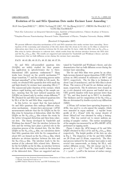
CHIN.PHYS.LETT.Vol.25,No.1(2008)242 Evolution of Ge and SiGe Quantum Dots under Excimer Laser Annealing∗HAN Gen-Quan(韩根全)1∗∗,ZENG Yu-Gang(曾玉刚)1,YU Jin-Zhong(余金中)1,CHENG Bu-Wen(成步文)1,YANG Hai-Tao(杨海涛)21State Key Laboratory on Integrated Optoelectronics,Institute of Semiconductors,Chinese Academy of Sciences,Beijing1000832Tsinghua-Foxconn Nanotechnology Research Center,Department of Physics,Tsinghua University,Beijing100084(Received15September2007)We present different relaxation mechanisms of Ge and SiGe quantum dots under excimer laser annealing.Inves-tigation of the coarsening and relaxation of the dots shows that the strain in Ge dots on Gefilms is relaxed by dislocation since there is no interface between the Ge dots and the Ge layer,while the SiGe dots on Si0.77Ge0.23film relax by lattice distortion to coherent dots,which results from the obvious interface between the SiGe dots and the Si0.77Ge0.23film.The results are suggested and sustained by Vanderbilt and Wickham’s theory,and also demonstrate that no bulk diffusion occurs during the excimer laser annealing.PACS:68.65.Hb,68.35.Fx,68.35.Md,68.37.PsGe and SiGe self-assembled quantum dots (SAQDs)are widely studied for their promis-ing application in optoelectronics due to three-dimensional(3D)quantum confinement.[1]Many works have focused on the growth mechanism,[2,3] shape transition,[4,5]and the coarsening process under thermal annealing[6]of the SAQDs in S-K mode.Re-cently,we obtained SiGe quantum dots with small size and high density by excimer laser annealing(ELA).[7] The nanosecond pulse duration of the excimer,which induces rapid heating and cooling of the sample sur-face,ensuring that the laser induced quantum dots (LIQDs)are formed only by surface atoms diffusion.[8] We obtained Ge and SiGe laser induced quantum dots by ELA of the Ge and SiGefilms,respectively.In this Letter,we report that the laser-induced Ge and SiGe quantum dots undergo different relax-ation mechanisms.Atomic-force-microscopy(AFM) measurements indicate that the Ge LIQDs on the Ge film relax by formation of dislocation,while the SiGe LIQDs on the Si0.77Ge0.23film release the strain by the lattice tetragonal distortion and then form coher-ent dots.The theory developed by Vanderbilt and Wickham has shown[9]that the interface between the dots and the wetting layer plays a pivotal role in the relaxation process of the strained dots.For the SiGe LIQDs on the Si0.77Ge0.23film,our calculation shows that SiGe quantum dots with the Ge composition of about83%are formed on the Si0.77Ge0.23film,which indicates an obvious interface between the dots and the Si0.77Ge0.23film.The interface leads to the for-mation of the coherent SiGe relaxed dots.However, for the Ge LIQDs on the Gefilm,no interface between the dots and the wetting layer results in the formation of the dislocated dots.These are suggested and sus-tained by Vanderbilt and Wickham’s theory,and also demonstrates that no bulk diffusion occurs during the excimer laser annealing.The Ge and SiGefilms were grown by an ultra-high-vacuum chemical vapour deposition(UHV-CVD) system on(001)-oriented Si substrates at500◦C and 550◦C,respectively.The Gefilm is in thickness of about1nm(8monolayers),and the SiGefilm is about 20nm.The sources of Si and Ge are disilane and ger-mane,respectively.The Si substrates were cleaned in an ex-situ chemical etch process and loaded into an UHV growth chamber with basic pressure lower than 10−7Pa,and then heated up to950◦C to deoxidize. The thickness and Ge composition of the Si0.77Ge0.23film are determined by double-crystal x-ray diffraction (XRD).A193nm ArF excimer laser operating frequency in 40Hz,was used to ex-situ anneal the samples,which were annealed in argon ambient.A top-flat beam profile of10×10mm2with the energy density of about180mJ/cm2was obtained by using a homog-enizer.This was carried out to ensure uniform an-nealing of samples’surface.The surface morphology of the samples was measured by an SPA-300HV AFM, performed in tapping mode.Figure1shows the AFM images of Ge and SiGe LIQDs obtained by ELA of Ge and Si0.77Ge0.23films, respectively.The height profiles of the dots are also in Fig.1.The diameters of the Ge and SiGe LIQDs are20–25nm and15–20nm,respectively.The ther-mal process induced by the excimer laser pulse is only several tens nanoseconds,so during the ELA,only surface diffusion occurs.The dot energy can be ex-pressed by E=4ΓV2/3tan1/3θ−6AV tanθ,[2]where Γ=γd cscθ−γs cotθis the increase of surface energy,∗Supported by the National Natural Science Foundation of China under Grant No60576001.∗∗Email:hgquan@c 2008Chinese Physical Society and IOP Publishing LtdNo.1HANGen-Quan et al.243γs and γd are the surface energy per unit area of the wetting layer and dot facet,respectively,θis the facet angle with respect to the surface of the wetting layer,V is the volume of the dot,A =σ2(1−ν)/(2πG )where σis the in-plane misfit strain,and νand G are Poisson’s ratio and shear modulus,respectively.For the LIQDs,only surface energy should be stud-ied,and the second term on the right can be con-sidered as the effect of strain on the surface energy.From the formula,we can see that the slightly strained dots are not stable during the ELA.We speculate that the heavily strained LIQDs will grow,relax the strainin them with longer annealing time.To investigate the relaxation of the LIQDs,we prolong the anneal-ing time with the laser energy density of 180mJ/cm 2.As the ELA continues,We observe the relaxation and the shrinking of the LIQDs,while it is surprisingly found that Ge quantum dots on the Ge wetting layer and SiGe dots on the Si 0.77Ge 0.23layer underwent the different relaxation modes:the Ge dots relax through the formation of the dislocation,while the strain in the SiGe quantum dots on the Si 0.77Ge 0.23wetting layer is released by lattice tetragonal distortion.Fig.1.AFM images (500nm ×500nm)of LIQDs:(a)Ge LIQDs on the Ge film and the height profiles along the line marked,(b)SiGe LIQDs on the Si 0.77Ge 0.23film and the height profiles along the line marked.Figure 2shows a series of AFM images of the mor-phology of Ge LIQDs on the Ge film at different an-nealing times.When the annealing time is prolonged to 3.5hours,coarsening of the quantum dot,as shown in Fig.2(a),occurs.The contacting of the small and large dots in Fig.2(a)and 2(b)can be interpreted to be the losing materials of small dots to the near large dots,which is analogous to the anomalous coarsening in the SAQDs.[10]As the ELA proceeds,the density of the dots further decreases,and when the annealing time is up to 5hours,almost all the LIQDs disappear (shown in Fig.2(c)).After 7-h ELA,no new LIQDs are observed.We speculate that the relaxation of the laser induced Ge dots is by the dislocations and the strained film is also relaxed by the dislocations.Fig-ure 3shows the schematic of the relaxation process ofthe Ge quantum dots on the Ge film.Figure 4(a)shows the coarsening and the growth of the SiGe dots on the Si 0.77Ge 0.23film.After 4-h an-nealing,the SiGe dots become larger and the density decreases.As the annealing continues (5h),some new LIQDs appear.This indicates that the growth and disappearing of the SiGe dots give rise to the restora-tion of the strain in the Si 0.77Ge 0.23film.This will decrease the surface energy and increase the strain en-ergy.The recovered stress in the film drives the new LIQDs under ELA.This reveals that the SiGe dots grow and relax to be the coherent dots,i.e.,the strain in the SiGe dots is relaxed by the lattice distortion.Figure 5shows the schematic of the relaxation process of the SiGe quantum dots on the Si 0.77Ge 0.23film.244HAN Gen-Quan et al.Vol.25Fig.2.AFM images (1µm ×1µm)of the Ge LIQDs on the Ge film with different annealing times:(a)annealed for 3.5h,(b)annealed for 4h,(c)annealed for 5h,(d)annealed for 7h.Fig.3.Schematic diagram of the relaxation mode of the Ge quantum dots on the Ge film.Fig.4.AFM images (1µm ×1µm)of the SiGe LIQDs on the Si 0.77Ge 0.23film for different annealing times:(a)annealed for 4h,(b)annealed for 5h.These results reveal the existence of two different relaxation mechanisms:generation dislocation in the dots and formation coherent relaxed dots.When the quantum dots grow,the relaxation of quantum dots is the competing of the lattice distortion (coherent re-laxed dots)with the formation of the dislocation (dis-located relaxed dots).The theory developed by Van-derbilt and Wickham [9]compares the two mechanisms of elastic relaxation and yields a phase diagram of a lattice mismatched system in which all possible mor-phologies are present,i.e.,uniform films,dislocated dots,and coherent dots.No.1HAN Gen-Quan et al.245It was shown by Vanderbilt and Wickham that morphology of the mismatched system is determined by the ratio of the energy of interface between dots and the wetting layer (E interface )to the change of the sur-face energy (∆E surf ).[9]The deposited material wets the substrate firstly,and then the 2D strained film transforms to the 3D quantum dots.If ∆E surf is posi-tive and large,or if the energy of the interface between the dots and the wetting layer is relatively small,the formation of coherently strained dots is not favoured.With an increase in the amount of deposited material,a transition occurs from uniform film to dislocated dots,and the coherently strained dots are not formed.If ∆E surf is positive and small,or if the energy of the dislocated interface is relatively large,with an increase in the amount of deposited material,a transition oc-curs from a uniform film to coherent dots.Further de-position may cause the onset of dislocations.The de-tailed calculation and the phase diagram can be found in Ref.[9].Fig.5.Schematic diagram of the relaxation process of the SiGe quantum dots on the Si 0.77Ge 0.23film.This theory can be used to interpret the differ-ent relaxation modes of the Ge and SiGe dots.It is sure that the pyramidal laser induced Ge dots,with the diameter of about 20–25nm and density of about 6×1010cm −2,do not exhaust the Ge film with the thickness more than 1nm (8monolayers).Because no bulk diffusion occurs during the annealing,atoms intermixing between the dots and the wetting layer need not be considered.We think that the pure Ge LIQDs are formed on the Ge film,i.e.,there is no in-terface between the dots and the wetting layer.For the SiGe LIQDs on the Si 0.77Ge 0.23film,based on the surface chemical potential calculation,we show that the heavily strained SiGe quantum dots must have a misfit above 0.035corresponding to a Ge composi-tion of about 83%,to promise E surf <0(the dots stable under ELA).[7]This indicates the SiGe dots are Ge richer than the Si 0.77Ge 0.23film,which also results from that the surface diffusion coefficient of Ge is 102–103times greater than that of Si.[11]If the atoms interdiffusion is neglected,there should be an obvious interface between the SiGe quantum dots and the Si 0.77Ge 0.23wetting layer.It is suggested theoret-ically by Vanderbilt and Wickham and supported by our experiments that the interface between the quan-tum dots and the wetting layer plays a pivotal role in the competition between the lattice distortion and the formation of dislocation.Vanderbilt and Wickham’s theory is proven by our results and also confirms and enforces our previous conclusion that the pure Ge dots and an abrupt inter-face between the dots and wetting layer are availablewhich is attributed to no bulk atoms diffusion under ELA.In conclusion,we have studied the different relax-ation mechanisms of the Ge and SiGe quantum dots on Ge and Si 0.77Ge 0.23films,respectively,under ELA.We recover the pivotal role of the interface between the dots and the wetting layer.The relaxation of Ge dots by dislocation is attributed to no interface between Ge dots and the Ge layer,and that of SiGe dots by lattice tetragonal distortion results from the obvious interface between SiGe dots and the Si 0.77Ge 0.23film.This is sustained by Vanderbilt and Wickham’s theory.References[1]Baribeau J M,Wu X,Rowell N L and Lockwood D J 2006J.Phys.:Condens.Matter 18R139[2]TersoffJ and LeGoues F K 1994Phys.Rev.Lett.723570[3]Sutter P,Schick I,Ernst W and Sutter E 2003Phys.Rev.Lett.91176102[4]Rastelli A,Stoffel M,TersoffJ,Kar G S and Schimidt O G2005Phys.Rev.Lett.95026103[5]Montalenti F,Raiteri P,Migas D B,von K¨a nel H,RastelliA,Manzano C,Costantini G,Denker U,Schimidt O G,Kern K and Miglio L 2004Phys.Rev.Lett.93216102[6]Kamins T I,Medeiros-Ribeiro G,Ohlberg D A A andWilliams R S 1999J.Appl.Phys.851159[7]Han G Q,Zeng Y G,Yu J Z,Cheng B W and Yang H T2007J.Cryst.Growth (submitted)[8]Misra N,Xu L,Pan Y L,Cheung N and Grigoropoulos CP 2007Appl.Phys.Lett.90111111[9]Vanderbilt D and Wickham L K 1991Mater.Res.Soc.Symp.Proc.202555[10]Rastelli A,Stoffel M,TersoffJ,Kar G S and Schmidt O G2005Phys.Rev.Lett.95026103[11]Huang L,Liu F,Lu G-H and Gong X G 2000Phys.Rev.Lett.96016103。
荧光粉的制备

Tunable color temperature solid state white light source using flux grown phosphor crystals of Eu 3+,Dy 3+and Tb 3+activated calcium sodium molybdenumoxideA.Khanna,P.S.Dutta ⇑Smart Lighting Engineering Research Center,Rensselaer Polytechnic Institute,Troy,NY 12180,USAElectrical,Computer and Systems Engineering Department,Rensselaer Polytechnic Institute,Troy,NY 12180,USAa r t i c l e i n f o Article history:Received 20January 2014Received in revised form 14July 2014Accepted 7August 2014Available online 10September 2014Keywords:PhosphorsFlux crystal growth White LEDsColor temperaturea b s t r a c tSolid state light sources with dynamically tunable color temperature in the range of 3000–6000K with chromaticity coordinates lying on the Planckian black body curve has been designed using mixtures of narrow emissions at 615nm,575nm and 550nm.These respective emissions lines were generated by individual phosphor crystals of trivalent rare earth (RE 3+)species,europium (Eu 3+),dysprosium (Dy 3+)and terbium (Tb 3+)activated calcium sodium molybdenum oxide (Ca 1À2x Na x MoO 4:RE 3+x ),when excited by near-ultra-violet (NUV)light emitting diode (LED)with emission wavelength of 380nm.Highly lumi-nescent crystals of these compounds have been grown from molten solutions (flux)of molybdenum (VI)oxide.The flux grown crystals exhibit emission intensity 2–4times more than phosphor powders of the same compounds synthesized by traditional solid-state reactions.An optimum flux to solute ratio of 2.5and solute dissolution temperature of 1100°C resulted in the largest size crystals.Ó2014Elsevier B.V.All rights reserved.1.IntroductionDynamic color tunable solid state light sources form the back-bone of future smart lighting systems for a wide variety of applica-tions.The design of such lighting systems with precise and easy color tunability could tremendously benefit from the availability of individual sources with narrow emission spectral characteris-tics.For general illumination applications,the preference for color temperature of the white light is dependent on many factors such as the space/ambient to be lit and the cultural background of the people.One such study that is being thought by smart lighting designers for enhancing human productivity (and alertness)at work place is by dynamically controlling color temperature from cool white ($6000K)to warm white ($3000K)depending on the time of the day.This paper presents a plausible pathway for designing dynamically controllable light sources using narrow emission phosphor crystals in conjunction with GaInN NUV-LEDs.Phosphors based on alkaline earth metal molybdate compounds provide potential host lattice for trivalent lanthanide ions (such as Eu 3+,Tb 3+,Dy 3+,Pr 3+and Sm 3+)and exhibit efficient energy transferfrom tetragonal molybdate groups (MoO 42À)to the trivalentlanthanide activator for narrow line-width emission [1–7].These phosphors have been studied in the past for fluorescent lamps and were found to be suitable candidates.For applications in LEDs,to-date they have been found to be less attractive due to their poor absorption of the light in the wavelength range of 380–470nm where the highest efficiency commercial NUV or blue LEDs emit.The absorption characteristics are limited to narrow f–f transitions of the activator ions.Of the lanthanide activators,studies on Eu 3+have been mostly conducted and reported due to the interest in narrow line red emitting phosphor for high CRI warm white LEDs.Various synthesis processes such as sol–gel and hydrothermal growth,charge compensation and structural modification around the Eu 3+lattice site by substitution of mono-valent alkali metal cations (Li +,Na +,K +)have been attempted to increase the intensity of Eu 3+f–f transitions in alkaline earth metal molybdate com-pounds and the photoluminescence intensity [7–14].In the present study,a flux crystal growth process has been established to grow optically clear crystals of alkaline earth metal molybdate phos-phors with the goal of improving its NUV/blue wavelength excit-ability,quantum efficiency and light extraction efficiency.With optically transparent crystals,one could increase the optical absorption path length as well as reduce light scattering compared to traditional phosphor powders used in ing three separate crystals of Ca 1À2x Na x MoO 4:RE 3+x with RE 3+species of Eu 3+,Dy 3+and Tb 3+as activators and Na +as the charge compensation species,color tunable solid state light sources have been discussed./10.1016/j.optmat.2014.08.0090925-3467/Ó2014Elsevier B.V.All rights reserved.⇑Corresponding author at:Smart Lighting Engineering Research Center,Rensselaer Polytechnic Institute,Troy,NY 12180,USA.E-mail address:duttap@ (P.S.Dutta).2.Experimental detailsBased on the prior studies [15],molybdenum (VI)oxide has been used as the flux (solvent)for crystal growth experiments due to its low melting point ($800°C),and high solubilities of alkaline earth metal molybdates,trivalent activators (Eu 3+,Dy 3+,Tb 3+)and charge compensation species (Na +)in the solvent.The choice of Na +as the charge compensation species over other group IA species (Li +or K +)was based on the similarity of ionic radii of the charge compensator ion Na +(116pm)and the alkaline earth metal cation to be replaced i.e.Ca 2+(114pm).Charge compensation in CaMoO 4is represented by the stoichiometric equation,2A 2+?RE 3++B +,wherein B +is the compensating ion,A 2+is the alkaline earth metal cation and RE 3+is the rare earth activator ion.Only Eu 3+ions that are incorporated at the divalent Ca 2+sites i.e.activated can contribute to photoluminescence.In the absence of the charge compensator,trivalent rare earth ions (RE 3+)cannot be efficiently activated on the divalent Ca 2+lattice sites and there-fore,only a small portion of RE 3+ions in the composition is respon-sible for the emission.Also,Eu 3+615nm emission is a result of the partially forbidden transition,which becomes more probable with increasing asymmetry around Eu 3+ion.Thus,the replacement of Ca 2+ions with the charge compensator B +aids the formation of an asymmetric environment for the Eu 3+615nm emission.This is yet another reason for the improvement in luminescence inten-sity with the introduction of charge compensator in the matrix.Generally,a compensator ion with radius similar to the alkaline earth metal cation would exhibit higher solubility in the host lat-tice.Therefore,Na +can effectively replace Ca 2+ions in CaMoO 4and also activate an equal number of RE 3+ions on the divalent sites via charge compensation.The role of alkaline earth metal cations (A 2+=Ca 2+,Sr 2+,Mg 2+)on the luminescence characteristics will also be presented for the case of Eu 3+activated phosphor crystals.The powder precursors used in our experiments were obtained from Alfa Aesar company.The following precursors were used with purity levels as indicated in brackets:Mg(OH)2(95%),CaO (99.95%),SrO (99.5%),Na 2CO 3(98%),MoO 3(99.8%),Eu 2O 3(99.9%),Tb 4O 7(99.9%)and Dy 2O 3(99.9%).The molar concentration of the RE 3+acti-vators was chosen to be around the optimum value of 12,2and 5mol%for Eu 3+,Dy 3+,Tb 3+,respectively,based on our prior research [15].For the phosphor crystal growth experiments,the precursors in the molar ratios and the excess flux species (molybdenum (VI)oxide)were homogenized for 30min at 600rpm using a Retsch PM 100Planetary Ball Mill.These powders were then transferred to alumina crucibles inside a box furnace in oxygen ambient and heated to high temperature for synthesis and crystal growth.The flux dissolution temperature was chosen as 1100°C based on the trade-off for rapid loss of elemental molybdenum species from the molten solution at higher temperatures (boiling point of MoO 3-$1150°C)and lower solubility of the precursors in the flux at lower temperatures [15].Based on extensive experimentation,dissolution time of 24h at 1100°C was found to be sufficient for complete anduniform reaction.Thereafter the solution was cooled at a rate of 3°C/h from 1100°C to 650°C,which is below the melting point of the flux ($800°C).Crystals are grown by the self-nucleation process inside the flux due to increasing supersaturation in the solution with decreasing temperature (as the solubility of precursors in the flux decreases with temperature).The temperature of the crystal-flux matrix is cooled slowly till 650°C even after the residual flux solid-ifies ($800°C)to avoid cracking of the crystals due to thermal expansion and shock.Below 650°C,the furnace was cooled at a rate of 350°C/h to room temperature.The crystals embedded inside the flux are extracted by dissolving the excess flux in hot water for 1–2h followed by mild HCl–water mixture (pH $2).The size of the crys-tals varies by the flux to solute ratio for a given dissolution temper-ature as well as cooling rate during the crystal growth.Table 1summarizes the size of Ca 0.76MoO 4:Eu 0.123+/Na 0.12+crystals grown with different flux-to-solute ratios for the growth conditions dis-cussed above.It is seen that a flux-to-solute ratio of 2.5gives rise to the largest crystal dimensions (4Â3Â2mm 3)for Ca 0.76MoO 4:Eu 0.123+/Na 0.12+phosphors.Further,the flux-to-solute ratio of 2.5wasused for growth of A 0.76MoO 4:Eu 0.123+/Na 0.12+(A =Mg,Sr),Ca 0.9MoO 4:Dy 0.053+/Na 0.05+and Ca 0.96MoO 4:Tb 0.023+/Na 0.02+crystals.The sizes of the resulting crystals are listed in Table 1.Photos of the flux grown phosphor crystals are illustrated in Fig.1(a–e).For comparison of the luminescence properties of the flux grown phosphor crystals with phosphor powders of the same composi-tions,traditional solid state reaction process was used to synthesize the powders.The phosphor powders were synthesized with and without the Na +charge compensation to understand the role of charge compensation on the excitation and emission characteris-tics.For solid state reactions,there was no excess flux of MoO 3in the starting powder.The homogenized powders (following the same process as above)were reacted in quartz crucibles at 1100°C for 24h followed by rapid cooling to room temperature at a rate of 350°C/h.Free flowing phosphor powders were obtained after the reaction.The excess MoO 3flux tends to severely react with quartz crucibles and hence could not be used for crystals growth.However for solid state reactions,they were found to be adequate.Powder X-ray diffraction (XRD)data was recorded using Bruker D8Discover Diffractometer running on Cu K a radiation at 40kV and 40mA.The XRD patterns were used for crystal structure deter-mination of the synthesized phosphors and the lattice parameters were calculated.Photoluminescence excitation and emission spec-trum were obtained using a Flourolog Tau-3lifetime measurement system.The chromaticity coordinates of phosphors crystals were characterized using an Ocean Optics Spectrometer (Jazz Spectros-copy Suite)and Spectrasuite software.For these measurements,the crystals were cleaved into smaller pieces and suspended in a two-part silicone matrix (RTV 6126A and B).This was necessary to ensure the same optical path length of the light in various sam-ples.Phosphor crystals suspended in silicone were dispensed on the bare LED die (1mm Â1mm surface area)and spread out to obtain a thin film with an equivalent phosphor density of 1mg/mm 2.The micro-crystals embedded in silicone were cured in nor-mal air atmosphere at room temperature for 24h.The 380nm GaInN NUV LEDs were used as the excitation source for the mea-surements of the chromaticity coordinates.3.Results and discussion 3.1.Crystal structureFig.2(a)shows the powder XRD patterns for the phosphors reported in this paper along with the patterns obtained from JCPDSdatabase for these compounds.The Ca 0.76MoO 4:Eu 0.123+/Na 0.12+,Sr 0.76MoO 4:Eu 0.123+/Na 0.12+,Ca 0.9MoO 4:Dy 0.053+/Na 0.05+and Ca 0.96MoO 4:Tb 0.023+/Na 0.02+phosphors exhibit tetragonal crystal structure and all theTable 1Sizes of flux grown phosphor crystals with different flux-to-solute ratios.PhosphorFlux-solute molar ratio Crystal size (mm 3)Ca 0.76MoO 4:Eu 0.123+/Na 0.12+1:12Â1Â1Ca 0.76MoO 4:Eu 0.123+/Na 0.12+ 1.5:12Â2Â1Ca 0.76MoO 4:Eu 0.123+/Na 0.12+2:13Â2Â2Ca 0.76MoO 4:Eu 0.123+/Na 0.12+ 2.5:14Â3Â2Ca 0.76MoO 4:Eu 0.123+/Na 0.12+3:12Â1Â1Ca 0.76MoO 4:Eu 0.123+/Na 0.12+4:11Â1Â1Mg 0.76MoO 4:Eu 3+0.12/Na +0.122.5:12Â2Â1Ca 0.76MoO 4:Eu 3+0.12/Na +0.124Â3Â2Sr 0.76MoO 4:Eu 3+0.12/Na +0.122Â1Â1Ca 0.9MoO 4:Dy 3+0.05/Na +0.053Â2Â1Ca 0.96MoO 4:Tb 3+0.02/Na +0.023Â2Â2A.Khanna,P.S.Dutta /Optical Materials 37(2014)646–655647peaks in XRD patterns could be indexed to JCPDS cards 00-029-0351,00-008-0482and 00-029-0351,respectively.Mg 0.76MoO 4:Eu 0.123+/Na 0.12+phosphors exhibit monoclinic crystal structure and the XRD peaks can be indexed to JCPDS card 01-072-2153.The tetragonal and monoclinic crystal structures for these alkaline earth metal molybdates are shown in Fig.2(b and c).As seen from Fig.2(b),in the monoclinic structure,transition metal ion undergoes octahedralco-ordination with oxygen (MoO 66Àgroup)as opposed to tetrahedralcoordination in the tetragonal structure (MoO 42Àgroup).Since oxy-gen coordinated group of transition metal ion give rise to specific excitation characteristics (as discussed below),the co-ordination number is an important parameter affecting the photoluminescence properties of these compounds.The lattice constants calculated from the XRD data were found to match closely with the values from the JCPDS database (Table 2).Hence it was concluded that the phosphors possess appropriate phase purity.No extraneous peaks (resulting from un-reacted species)were found in the XRD patterns implying that the activator ions were uniformly incorporated in the crystal lattice.3.2.Excitation spectraThe excitation spectra of A 0.76MoO 4:Eu 0.123+/Na 0.12+(A =Ca,Mg,Sr),Ca 0.9MoO 4:Dy 0.053+/Na 0.05+and Ca 0.96MoO 4:Tb 0.023+/Na 0.02+phosphor crystals for their narrow line emission wavelengths of 615nm,575nm and 550nm,respectively,are shown in Fig.3(a–c).Each spectrum consists of two regions:a broad excitation band in the wavelength range of 290–350nm resulting from the charge trans-fer excitation (also known as charge transfer band or CTB)of MoO x groups (x =4for A =Ca,Sr;x =6for A =Mg)and a series of narrow excitation peaks in the wavelength range of 350–550nm corre-sponding to f–f transitions of the trivalent lanthanide activator (Eu 3+,Dy 3+,Tb 3+)[2,3,15].As seen in Fig.3(a),the peak of the CTB is shifted towards the longer wavelength for AMoO 4(A =Mg,Sr)with respect to the peak of the CaMoO 4phosphor.The shift in CTB peak for MgMoO 4phos-phors can be explained in terms of octahedral co-ordination of Mo 6+ion in a monoclinic structure depicted in Fig.2(b)as opposed to tetrahedral co-ordination in tetragonal molybdates (A =Ca,Sr)shown in Fig.2(c).When Mo 6+undergoes octahedral co-ordination,longer Mo 6+–O 2Àbonds are required to accommodate six O 2Àions on account of small ionic radius (59pm)of Mo 6+.Longer bonds lower the energy gap of the molybdate host leading to the shift in CTB exci-tation to longer wavelengths.The CTB peak shift in SrMoO 4resultsfrom weaker crystal field experienced by Mo 6+in SrMoO 4as com-pared to the crystal field experienced by Mo 6+in CaMoO 4and this lowers the host energy gap and thus the CTB excitation energy [16].The weaker crystal field in SrMoO 4is a result of larger ionic radius of Sr 2+(118pm)as compared to Ca 2+(114pm)and thus,longer unit cell dimensions.3.3.Emission spectraThe emission spectra for A 0.76MoO 4:Eu 0.123+/Na 0.12+(A =Ca,Mg,Sr),Ca 0.9MoO 4:Dy 0.053+/Na 0.05+and Ca 0.96MoO 4:Tb 0.023+/Na 0.02+phosphor crystals are presented at the excitation wavelength of 380nm in Fig.4.As seen in Fig.4,the emission spectra of A 0.76MoO 4:Eu 0.123+/Na 0.12+(A =Ca,Mg,Sr)phosphors exhibit the typical Eu 3+narrow line emissions at 615nm (electric-dipole),536,592(magnetic-dipole)and 652nm corresponding to (5D J –7D 0,J =0,1)?(7F 0–7F J ,J =1,2,3,4)transitions.The electric dipole transition (5D 0?7F 2)at 615nm is the dominant peak in the emission spectrum,which is expected due to lack of inversion symmetry in the crystal struc-ture of these phosphors.Also,due to lack of inversion symmetry,the magnetic dipole transition at 592nm (5D 0?7F 1)is almost 10times weaker in intensity as compared to the electric dipole tran-sition.Also,in addition to the Eu 3+f–f transitions,the emission spectra consist of a host emission broad band centered around 430nm.As seen from Fig.4,the host emission intensity is highest for SrMoO 4:Eu 3+and weakest for CaMoO 4:Eu 3+phosphors.The host emission is exhibited by alkaline earth metal molybdates due tothe presence of tetrahedral MoO 42Àand octahedral MoO 66Àgroups.It was found that the host emission characteristics depended sig-nificantly upon the co-ordination environment of Mo 6+in these compounds and the differences with varying alkaline earth metal cation were studied in detail.In order to investigate the host emission spectra (with peak around 430nm),further characterization was done for excitation wavelength as shown in Fig.5(a).The excitation wavelength of 370nm was found to be suitable for isolating the contribution of host in the emission spectrum since Eu 3+does not have an excita-tion peak resulting from f to f transitions at 370nm as confirmed from Fig.3(a).The emission spectra for the host emission at 430nm were also recorded and are depicted in Fig.5(b).CaMoO 4phosphor exhibits the shortest peak wavelength of emission and excitation (k peak )in Fig.5(a and b).It is clear from Fig.3(a)and Fig.5(a and b)that the energy gap and CTB energy increase while host excitation and host emission wavelength range decreaseinof (a)Mg 0.76MoO 4:Eu 0.123+/Na 0.12+,(b)Ca 0.76MoO 4:Eu 0.123+/Na 0.12+,(c)Sr 0.76MoO 4:Eu 0.123+/Na 0.12+,(d)Ca 0.9MoO 4:Dy 0.053+/Na 0.05+the given order for alkaline earth metal cations:Mg 2+,Sr 2+,Ca 2+.This trend results from the difference in the co-ordination environ-ment of Mo 6+ion in the molybdates of these ions as shown in Fig.5(b).Therefore,the energy gap (CTB excitation energy)is high-est for CaMoO 4due to the shorter Mo 6+–O 2Àbonds as compared to magnesium and strontium molybdate,resulting in a blue shift in the host excitation and emission bands observed for the CaMoO 4:Eu 3+phosphor.Table 3summarizes the host excitation andemission characteristics of A 0.76MoO 4:Eu 0.123+/Na 0.12+(A =Ca,Mg,Sr)phosphors.Amongst the three AMoO 4(A =Mg,Ca,Sr)phosphors,emission intensity (at 615nm)is maximum for CaMoO 4:Eu 3+phosphor as seen in Fig.4.For 12%Eu 3+dopant concentration,the number of Eu 3+ions per unit volume decreases in the order CaMoO 4<MgMoO 4<SrMoO 4.Therefore,CaMoO 4accommodates the highest number of dopant ions (Eu 3+)which results in an efficient energy transfer from host to activator for f–f transitions.This is the reasonfor the observance of maximum luminescence intensity in CaMoO 4amongst the AMoO 4phosphors.Further,it is seen from Fig.5(a and b)that the host emission intensity and ratio of host to activator emission intensity is highest for MgMoO 4:Eu 3+phosphor and the ratio of host to activator emission intensity decreases in the follow-ing order,MgMoO 4>SrMoO 4>CaMoO 4.The band gap of the molybdates follows an exactly opposite trend i.e.MgMoO 4(3.1–3.6eV)<SrMoO 4(3.72eV)<CaMoO 4(5.07eV),which can be attributed to the weaker crystal field in SrMoO 4[16]and the monoclinic structure of MgMoO 4[17].Lower band gap can cause high absorbance (and re-emission)in the NUV range (360–400nm)and increase the intensity of host emission.The light re-emitted after NUV range (360–400nm)excitation is therefore,either a result of the host lattice emission or is transferred to Eu 3+for f–f transitions.The ratio of host to activator emission intensity in molybdates can thus,be used as an indicator of the efficiency of host to activator energy transfer.This means that the energy transfer efficiency and also the Eu 3+emission intensity should follow the following order,CaMoO 4>SrMoO 4>MgMoO 4,which is in agreement with the experimental results presented in Figs.4and 5(a and b).The emission spectra for Ca 0.76MoO 4:Ln 0.123+/Na 0.12+(Ln =Dy,Tb)phosphors are depicted in Fig.4at 380nm excitation wavelength and consist of narrow line-width emissions from 4F 9/2?6H J (J =9/2,11/2,13/2,15/2)and (5D 3?7F J ,J =3,4,5)transitions of Dy 3+and Tb 3+ions,respectively.Table 4summarizes the excitationand emission characteristics of A 0.76MoO 4:Eu 0.123+/Na 0.12+(A =Ca,Mg,Sr),Ca 0.9MoO 4:Dy 0.053+/Na 0.05+and Ca 0.96MoO 4:Tb 0.023+/Na 0.02+phosphors.As described in Section 2,these phosphors were synthesized with and without Na +for charge compensation and via solid state reaction and flux growth to study the impact of charge compensa-tion and crystal growth process on the luminescent properties of the phosphor material.The enhancement in phosphor excitation intensity with charge compensation and flux growth is depicted in Fig.6(a–e)and Fig.7(a–e)for AMoO 4:Eu 3+(A =Mg,Ca,Sr)and CaMoO 4:RE 3+(RE =Dy,Tb)phosphors.Tables 5and 6summarize the improvement observed with charge compensation and flux growth.This enhancement is attributed to efficient incorporation of activator species in the host lattice in the flux growth process.Higher excitation intensity in Na +compensated powder phosphors results from the increased degree of asymmetry around the RE 3+sites in the lattice.This leads to a higher probability of electric dipole transitions for which the RE 3+needs to occupy a non-centrosymmetric lattice site and hence higher emission intensities at the respective wavelengths (615,575and 550nm).3.4.Chromaticity coordinates of phosphor crystal LEDsFig.8(a–c)shows the intense emission from flux grown phosphorcrystals of Ca 0.76MoO 4:Eu 0.123+/Na 0.12+,Ca 0.9MoO 4:Dy 0.053+/Na 0.05+andCa 0.96MoO 4:Tb 0.023+/Na 0.02+when excited by 380nm NUV GaInN LEDs.Fig.9(a)presents the 1931CIE (x ,y )chromaticity coordinates ofCa 0.76MoO 4:Eu 0.123+/Na 0.12+,Ca 0.9MoO 4:Dy 0.053+/Na 0.05+and Ca 0.96MoO 4:Tb 0.023+/Na 0.02+phosphors encapsulated on 380nm NUV LEDs and measured while operating the NUV LEDs at 20mA current and 3.3V forward voltage.The chromaticity coordinates lie in red regionfor Ca 0.76MoO 4:Eu 3+0.12/Na +0.12(0.63,0.34)and in the purplish redregion for Mg 0.76MoO 4:Eu 3+0.12/Na +0.12(0.52,0.26)and Sr 0.76MoO 4:Eu 3+0.12/Na +0.12(0.54,0.25)phosphors which is expected from the host to activator emission ratio and relative emission intensity at 615nm as discussed above.Further,due to strong contribution from the hostto the emission spectrum for the Mg 0.76MoO 4:Eu 3+0.12/Na +0.12phosphor,the chromaticity coordinates show maximum deviation from the straight line joining the 380nm and 615nm point on the CIE (x ,y )color space.This also points towards the possibility of utilizinghost2.(a)XRD patterns of A 0.88MoO 4:Eu 0.123+(A =Mg,Ca,Sr),Ca 0.95MoO 4:Dy 0.053+0.98MoO 4:Tb 0.023+phosphors.Crystal structure of (b)MgMoO 4(monoclinic)and AMoO 4,A =Ca,Sr (tetragonal).Materials 37(2014)646–655649emission for shifting the coordinates in the desired direction by changing or adding a small concentration of alkaline earth metal cat-ion to the phosphor material.The chromaticity coordinates for Ca 0.9MoO 4:Dy 3+0.05/Na +0.05phos-phor sample are close to the white region (0.38,0.35)and were found in the green-yellow region (0.34,0.6)for the Ca 0.96MoO 4:Tb 3+0.02/Na +0.02phosphor sample.Ca 0.96MoO 4:Tb 3+0.02/Na +0.02coordinates also show deviation from the straight line joining the 380nm point and 550nm point in the color space which results from the charac-teristic Tb 3+emission at 580nm and 610nm as shown in Fig.4when excited by a 380nm wavelength source.The chromaticity coordi-nates obtained in these experiments using the phosphor crystals did not compromise the lumens output from these devices unlike the powder phosphors of the same compounds for similar color coordinates.The emission from the three LEDs fabricated withCa 0.96MoO 4:Tb 0.023+/Na 0.02+(LED A),Ca 0.9MoO 4:Dy 0.053+/Na 0.05+(LED B)and Ca 0.76MoO 4:Eu 0.123+/Na 0.12+(LED C)phosphors forms a color space in the CIE (x ,y )diagram wherein by varying the intensity of one or more LEDs,the color temperature and CRI of the white light source can be tuned.The color space is shown in Fig.9(a).It must also be mentioned that the color coordinates of the samples shown in Fig.9(a)can be shifted anywhere along a straight line between the 380nm point representing peak emission wavelength of the LED excitation source and the peak emission wavelength of the individ-ual phosphor (615,575and 550nm)on the edge of the (x ,y )dia-gram.This can be done by altering the optical path length of the phosphor crystals mounted on the LED as shown in Fig.9(b).The various chromaticity points plotted by changing the phosphor opti-cal path length (A1–A5,B1–B5,C1–C5)in Fig.9(b)can further,be utilized to cover a range of color spaces represented by triangles drawn by joining the coordinates of the three LEDs.By appropriately choosing the points for drawing these triangles,it is possible toTable 2Lattice constants of AMoO 4:Eu 3+(A =Mg,Ca,Sr)and CaMoO 4:RE 3+(RE =Dy,Tb)phosphors calculated from the XRD data.PhosphorSynthesis processCrystal structureCalculated lattice constants JCPDS valuesa (nm)b (nm)c (nm)b (°)a (nm)b (nm)c (nm)b (°)Mg 0.88MoO 4:Eu 3+0.12SSR a Monoclinic1.0250.930.751061.0280.9290.702106.9Mg 0.76MoO 4:Eu 3+0.12/Na +0.12SSR 1.0250.950.69106.4Mg 0.76MoO 4:Eu 3+0.12/Na +0.12FG b 1.0270.950.71106.8Ca 0.88MoO 4:Eu 3+0.12SSR Tetragonal0.520.52 1.15900.5230.523 1.14390Ca 0.76MoO 4:Eu 3+0.12/Na +0.12SSR 0.5160.516 1.1690Ca 0.76MoO 4:Eu 3+0.12/Na +0.12FG 0.530.53 1.12990Sr 0.88MoO 4:Eu 3+0.12SSR Tetragonal0.5350.535 1.23900.5390.539 1.20290Sr 0.76MoO 4:Eu 3+0.12/Na +0.12SSR 0.5420.542 1.22900.76MoO 4:Eu 0.123+/Na 0.12+(A =Mg,Ca,Sr),(b)Ca 0.9MoO 4:Dy 0.053+/Na 0.05+and (c)Ca 0.96MoO 4:Tb 0.023+/Na 0.02+phosphors figures.650 A.Khanna,P.S.Dutta /Optical Materials 37(2014)646–655design dynamically tunable white light sources with desired colortemperature and CRI.Moreover,as seen from Fig.9(b)the triangle A5B1C5covers the maximum space and thus,by choosing this con-figuration,sources with the widest range of tunable color tempera-tures ranging from 2000K to 8000K can be fabricated.Next section describes two methods of using LEDs A5,B3and C5and the color space they cover for delivering tunable sources in the CCT range of 2000–6500K (warm white to cool white).3.5.Design of dynamically tunable white light sourcesThe three points A5(0.34,0.6),B3(0.33,0.26)and C5(0.63,0.34)enclose an important region in the white light space covering the blackbody Planckian Locus with color temperature in the approximate range of 6500K (cool white)to 2000K (warm white).important to point out that the choice of these three points are necessary for tuning the color coordinate precisely Planckian curve at different color temperatures while imizing the output lumens of the three individual devices (by imizing various losses in the phosphor such as optical scattering,absorption,quantum efficiency and Stokes shift).Examples tunable color white light sources using these LEDs will be be implemented by simultaneously increasing or decreasing the electrical power to the individual LEDs and will not be discussed here.3.5.1.White light source with same intensity,but tunable color Emission spectra of A 0.76MoO 4:Eu 0.123+/Na 0.12+(A =Mg,Ca,Sr),Ca 0.9/Na 0.05+and Ca 0.96MoO 4:Tb 0.023+/Na 0.02+phosphors recorded at 380nm excitation wavelength.spectra of A 0.76MoO 4:Eu 0.123+/Na 0.12+(A =Mg,Ca,Sr)recorded at the peak wavelength for host emission (k em –430nm)and Mg,Ca,Sr)phosphors.Table 3Photoluminescence properties of alkaline earth metal molybdate hosts (AMoO 4,A =Mg,Ca,Sr).Phosphork ex a (nm)k em b (nm)I host:activator c I 370d Mg 0.76MoO 4:Eu 3+0.12/Na +0.123704556:1 1.4Ca 0.76MoO 4:Eu 3+0.12/Na +0.12355435 4.8:11Sr 0.76MoO 4:Eu 3+0.12/Na +0.123654455.7:11.2ak ex –peak wavelength of host excitation band monitored at 430nm emission wavelength.bk em –peak wavelength of host emission band monitored at 370nm excitation wavelength.cI host:activator –ratio of host to Eu 3+emission intensity monitored at 370nm excitation wavelength.dI 370–host emission intensity monitored at 370nm excitation wavelength rel-ative to the host emission intensity of Mg 0.76MoO 4:Eu 3+0.12/Na +0.12phosphor.Table 4Photoluminescence properties of A 0.76MoO 4:Eu 3+0.12/Na +0.12(A =Mg,Ca,Sr),Ca 0.9MoO 4:Dy 3+0.05/Na +0.05and Ca 0.96MoO 4:Tb 3+0.02/Na +0.02phosphors.Phosphork CTB a (nm)I 380b Mg 0.76MoO 4:Eu 3+0.12/Na +0.123201Ca 0.76MoO 4:Eu 3+0.12/Na +0.12312 3.7Sr 0.76MoO 4:Eu 3+0.12/Na +0.123162Ca 0.9MoO 4:Dy 3+0.05/Na +0.053152Ca 0.96MoO 4:Tb 3+0.02/Na +0.023133.7ak CTB –peak of charge transfer band.bI 380–peak emission intensity monitored at 380nm excitation wavelengthrelative to the peak emission intensity of Mg 0.76MoO 4:Eu 3+0.12/Na +0.12phosphor.Materials 37(2014)646–655651。
MEMS课件-Chapter5-Addvances
Performance Factors
•Sensitivity: •Minimum amount of analyte that are able to be detected above the background •Units: Concentration, number of analyte, density, weight
Receptor: a sensing element that responds to the substances being measured, the interaction must be highly selective
Enzyme, Antibody, Nucleic acids, aptamer
Small molecules: Sugars, urea, cholesterol, glutamic acid, phosphate,.. Macro molecules : nucleic acids (DNA, RNA), peptide( protein, antibody, enzyme)
Clinical specificity measures the proportion of negatives which are correctly identified (e.g. the percentage of healthy people who are identified as not having the condition).
k1[S][E]-k-1[ES]-k2[ES]=0 As [E0]=[E]+[ES], k1[S][E0]-k1[S][ES]-k-1[ES]-k2[ES]=0
[ES] = k1[E0][S] = [E0][S]
碳量子点 英语

碳量子点英语Carbon quantum dots (CQDs) have attracted significant attention in recent years due to their unique properties and potential applications in various fields. These nanomaterials, which are typically less than 10 nanometers in size, possess excellent optical, electronic, and chemical properties,making them promising candidates for use in bioimaging, sensing, photocatalysis, and optoelectronic devices.One of the key advantages of CQDs is their exceptional photoluminescent properties. These nanomaterials exhibitstrong fluorescence, high photostability, and good biocompatibility, making them ideal for use in bioimaging and cellular labeling applications. Their ability to emit lightin the visible range makes them particularly useful for fluorescence imaging of biological samples.Furthermore, the tunable optical properties of CQDs have sparked interest in their potential for use in sensors and photodetectors. By adjusting the size, surface chemistry, and composition of CQDs, researchers can tailor their optical properties to create sensors for detecting various analytes, such as heavy metals, ions, and biomolecules. Additionally, the sensitivity and selectivity of CQD-based sensors can be enhanced through the incorporation of functional groups or specific ligands on their surface.In the field of photocatalysis, CQDs have shown promise as efficient catalysts for various chemical reactions, including the degradation of organic pollutants and the production of hydrogen through water splitting. Their high surface area, abundant surface functional groups, andefficient charge separation make them effective photocatalysts for driving these reactions under visiblelight irradiation.Moreover, CQDs have been explored for their potential use in optoelectronic devices, such as light-emitting diodes (LEDs) and solar cells. Their compatibility with solution processing techniques, low cost, and environmentally friendly nature make them attractive materials for realizing efficient and stable optoelectronic devices.In summary, the unique properties of CQDs make them versatile nanomaterials with promising applications in a wide range of fields. As research in this area continues to advance, it is expected that CQDs will play an increasingly important role in various technological and biomedical applications.。
(完整版)光伏行业英文词汇.docx
光伏行业英文词汇Cell 电池Crystalline silicon晶体硅Photovoltaic光伏bulk properties体特性at ambient temperature在室温下wavelength波长absorption coefficient吸收系数electron-hole pairs电子空穴对photon光子density密度defect缺陷surface表面electrode电极p-type for hole extraction p型空穴型n-type for electron extraction n型电子型majority carriers多数载流子minority carriers少数载流子surface recombination velocity ( SRV)表面复合速率back surface field(BSF)背场at the heavily doped regions重掺杂区saturation current density Jo饱和电流密度thickness厚度contact resistance 接触电阻concentration 浓度 boron 硼Gettering techniques 吸杂nonhomogeneous 非均匀的solubility溶解度selective contacts 选择性接触insulator 绝缘体oxygen 氧气hydrogen 氢气Plasma enhanced chemical vapor deposition PECVDInterface界面The limiting efficiency极限效率reflection反射light- trapping光陷intrinsic material本征材料bifacial cells双面电池monocrystalline单晶float zone material FZ- Si Czochralski silicon Cz- Si industrial cells工业电池a high concentration of oxygen 高浓度氧Block or ribbon块或硅带Crystal defects晶体缺陷grain boundaries晶界dislocation位错solar cell fabrication太阳能电池制造impurity杂质P gettering effect 磷吸杂效果 Spin-on 旋涂supersaturation过饱和dead layer死层electrically inactive phosphorus 非电活性磷interstitial空隙the eutectic temperature共融温度boron - doped substrate掺硼基体passivated emitter and rear locally diffused cells PERL电池losses 损失the front surface前表面metallization techniques金属化技术metal grids金属栅线laboratory cells实验室电池the metal lines金属线selective emitter选择性发射极photolithographic光刻gradient 斜度precipitate沉淀物localized contacts局部接触point contacts点接触passivated emitter rear totally diffused PERTsolder 焊接bare silicon裸硅片high refraction index高折射系数reflectance反射encapsulation封装antireflection coating ARC减反射层an optically thin dielectric layer 光学薄电介层interference effects干涉效应texturing制绒alkaline solutions碱溶液etch 刻蚀 / 腐蚀anisotropically各向异性地plane 晶面pyramids金字塔a few microns几微米etching time and temperature腐蚀时间和温度manufacturing process制造工艺process flow工艺流程high yield高产量starting material原材料solar grade太阳级a pseudo -square shape单晶型状saw damage removal去除损伤层fracture裂纹acid solutions酸溶液immerse 沉浸tank 槽texturization制绒microscopic pyramids 极小的金字塔size 尺寸大小hinder the formation of the contacts 阻碍电极的形成the concentration ,the temperature and the agitation of the solution 溶液的浓度,温度和搅拌the duration of the bath溶液维持时间alcohol酒精improve改进增加homogeneity 同质性wettability润湿性phosphorus diffusion磷扩散eliminate adsorbed metallic impurities消除吸附的金属杂质quartz furnaces石英炉quartz boats石英舟quartz tube石英炉管bubbling nitrogen through liquidPOCL3小氮belt furnaces链式炉back contact cell背电极电池reverse voltage反向电压reverse current反向电流amorphous glass of phospho -silicates非晶玻璃diluted HF稀释 HF溶液junction isolation结绝缘coin -stacked 堆放barrel -type reactors桶状反应腔fluorine氟fluorine compound 氟化物simultaneously同时地high throughput高产出ARC deposition减反层沉积Titanium dioxide TiO2Refraction index折射系数Encapsulated cell封装电池Atmospheric pressure chemical vapor deposition APCVDSprayed from a nozzle喷嘴喷雾Hydrolyze水解Spin - on 旋涂Front contact print正电极印刷The front metallization前面金属化Low contact resistance tosilicon 低接触电阻Low bulk resistivity低体电阻率Low line width with high aspect ratio低线宽高比Good mechanical adhesion好机械粘贴solderability可焊性screen printing丝网印刷comblike pattern梳妆图案finger指条bus bars主栅线viscous粘的solvent溶剂back contact print背电极印刷both silver and aluminum银铝form ohmic contact 形成欧姆接触warp 弯曲cofiring of metal contacts电极共烧organic components of the paste 浆料有机成分burn off烧掉sinter烧结perforate穿透testing and sorting 测试分选 I-V curve I-V 曲线Module 组件Inhomogeneous 不均匀的Gallium镓Degradation衰减A small segregation coefficient 小分凝系数Superposition重合The fourth quadrant第四象限The saturation current饱和电流 Io Fill factor填充因子 FF Graphically用图象表示The maximum theoretical FF理论上Empirically经验主义的Normalized Voc规范化 VocThe ideality factor n- factor理想因子Terrestrial solar cells地球上的电池At a temperature of 25C 25度下Under AM1.5 conditions在 AM1.5环境下Efficiency is defined as××定义为Fraction 分数Parasitic resistances寄生电阻Series resistance串联电阻Shunt resistance并联电阻The circuit diagram电路图Be sensitive to temperature易受Asymmetric 不对称的温度影响High resolution高分辨率The band gap of a semiconductor 半Base resistivity基体电阻率导体能隙The process flow工艺流程The intrinsic carrier Antireflection coating减反射层concentration 本征载流子的浓度Cross section of a solar cell太Reduce the optical losses减少光阳能电池横截面Dissipation损耗Light -generated current光生电流Incident photons入射光子The ideal short circuit flow理想短路电路The depletion region耗尽区Quantum efficiency量子效率Blue response 蓝光效应Spectral response光谱响应Light - generated carriers光生载流子Forward bias正向偏压Simulation模拟Equilibrium平衡损Deuterated silicon nitride含重氢氮化硅Buried contact solar cells BCSC Porous silicon PS多孔硅Electrochemical etching电化学腐蚀Screen printed SP丝网印刷A sheet resistance of 45-50 ohm/sq45 到 50 方块电阻The reverse saturation current density Job反向饱和电流密度Destructive interference相消干涉Surface textingInverted pyramid倒金字塔Four point probe四探Block-cast multicrystalline Saw damage etch silicon整多晶硅Alkaline 碱的Parasitic junction removal寄生Cut groove开槽的去除Conduction band Iodine ethanol碘酒Valence band 价Deionised water去离子水B and O simultaneously in silicon Viscosity粘性硼氧共存Mesh screen 网孔Iodine/methanol solution碘酒 / 甲Emulsion乳胶醇溶液Rheology 流学Properties of light光特性Spin -on dopants旋涂Electromagnetic radiation磁Spray -on dopants涂射The metallic impurities金属The visible light可光One slot for two wafers一个槽两The wavelength ,denoted by R 用 R 片表示波Throughput量An inverse relationship A standard POCL3 diffusion准between ⋯⋯ and ⋯⋯ given by thePOCL3散Back-to -back diffusion背靠背散Heterojunction with intrinsic thin -layer HIT 池Refine 提Dye sensitized solar cell染料敏化太阳池Organic thin film solar cell有机薄膜池Infra red外光Unltra violet紫外光Parasitic resistance寄生阻Theoretical efficiency理效率Busbar 主Kerf loss失Electric charge荷Covalent bonds 共价The coefficient of thermal expansion (CTE)膨系数Bump 鼓泡Alignment基准Fiducial mark基准符号Squeegee 橡胶Isotropic plasma texturing 各向等离子制equation :相反关系,可用方程表示Spectral irradiance分光照度⋯⋯is shown in the figure below. Directly convert electricity into sunlight 直接将成光Raise an electron to a higher energy state 子升入更高能External circuit外路Meta-stableLight-generated current光生流Sweep apart by the electric field Quantum efficiency量子效率The fourth quadrant第四象限The spectrum of the incident light 入射光The AM1.5 spectrumThe FF is defined as the ratio of ⋯⋯ to ⋯⋯Graphically 如所示Screen-printed solar cells网印刷池Phosphorous diffusion磷散A simple homongeneousdiffusion 均匀散Blue response光相Shallow emitter 浅结 Commercial production 商业生产Surface texturing to reduce reflection表面制绒Etch pyramids on the wafer surface with a chemical solutionCrystal orientationTitanium dioxide TiO2PasteInorganic无机的Glass 玻璃料DopantCompositionParticle sizeDistributionEtch SiNxContact pathSintering aidAdhesion 黏合性Ag powderMorphology 形态CrystallinityGlass effect on Ag/Siinterface Reference cellOrganicResin树脂Carrier载体Rheology 流变性Printability印刷性Aspect ratio高宽比Functional groupMolecular weightAdditives添加剂Surfactant表面活性剂Thixotropic agent触变剂Plasticizer可塑剂Solvent 溶剂Boiling pointVapor pressure蒸汽压Solubility溶解性Surface tension表面张力Solderability Viscosity黏性Solids contentFineness of grind,研磨细度Dried thicknessFired thicknessDrying profilePeak firing temp300 mesh screenEmulsion thickness乳胶厚度StorageShelf life保存期限Thinning稀释Eliminate Al bead formation消除铝珠Low bowingWet depositPattern design: 100um*74太阳电池solar cell单晶硅太阳电池single crystalline silicon solar cell多晶硅太阳电池so multi crystalline silicon solar cell非晶硅太阳电池amorphous silicon solar cell薄膜太能能电池Thin-film solar cell多结太阳电池multijunction solar cell化合物半导体太阳电池 compound semiconductor solar cell用化合物半导体材料制成的太阳电池带硅太阳电池 silicon ribbon solar cell光电子 photo-electron短路电流 short-circuit current (Isc)开路电压 open-circuit voltage (Voc)最大功率 maximum power (Pm)最大功率点maximum power point最佳工作点电压 optimum operating voltage (Vn)最佳工作点电流 optimum operating current (In)填充因子 fill factor(curve factor)曲线修正系数 curve correction coefficient太阳电池温度solar cell temperature串联电阻series resistance并联电阻 shunt resistance转换效率 cell efficiency暗电流 dark current暗特性曲线dark characteristic curve光谱响应 spectral response(spectral sensitivity)太阳电池组件 module(solar cell module)隔离二极管blocking diode旁路二极管bypass (shunt) diode组件的电池额定工作温度NOCT ( nominal operating cell temperature)短路电流的温度系数temperature coefficients of Isc开路电压的温度系数temperature coefficients of Voc峰值功率的温度系数temperature coefficients of Pm组件效率Module efficiency峰瓦 watts peak额定功率rated power额定电压rated voltage额定电流rated current太阳能光伏系统solar photovoltaic (PV) system并网太阳能光伏发电系统Grid-Connected PV system独立太阳能光伏发电系统Stand alone PV system太阳能控制器 solar controller逆变器 inverter孤岛效应islanding逆变器变换效率inverter efficiency方阵 (太阳电池方阵 ) array ( solar cell array)子方阵 sub-array (solar cell sub-array)充电控制器charge controller直流 / 直流电压变换器 DC/DC converter(inverter)直流 / 交流电压变换器 DC/AC converter(inverter)电网 grid irradiance (solar global irradiance)太阳跟踪控制器 sun-tracking ontroller辐射计 radiometer并网接口 utility interface方位角 Azimuth angle光伏系统有功功率 active power of PV倾斜角 Tilt anglepower station太阳常数 solar constant光伏系统无功功率reactive power of大气质量 (AM) air massPV power station光伏系统功率因数 power factor of PV太阳高度角 solar elevation angle power station标准太阳电池 standard solar cell 公共连接点 point of common coupling(reference solar cell)接线盒 junction box太阳模拟器 solar simulator发电量 power generation太阳电池的标准测试条件为:环境温输出功率 output power 度 25±2℃,用标准测量的光源辐照度为交流电 Alternating current1000W/m2 并且有标准的太阳光谱辐断路器 Circuit breaker照度分布。
2010-PhysRevLett.104.253603
PRL 104, 253603 (2010)
PHYSICAL REVIEW LETTERS get to the result [23]
PRL 104, 253603 (2010)
PHYSICAL REVIEW LETTERS
week ending 25 JUNE 2010
Differential Ghost Imaging
F. Ferri,* D. Magatti, L. A. Lugiato, and A. Gatti
` dell’Insubria, Via Valleggio 11, 22100 Como, Italy CNR-INFM-CNISM, Dipartimento di Fisica e Matematica, Universita (Received 5 February 2010; published 25 June 2010) We present a new technique, differential ghost imaging (DGI), which dramatically enhances the signalto-noise ratio (SNR) of imaging methods based on spatially correlated beams. DGI can measure the transmission function of an object in absolute units, with a SNR that can be orders of magnitude higher than the one achievable with the conventional ghost imaging (GI) analysis. This feature allows for the first time, to our knowledge, the imaging of weakly absorbing objects, which represents a breakthrough for GI applications. Theoretical analysis and experimental and numerical data assessing the performances of the technique are presented.
Fundamentals of Intensified CCD(ICCD)
Leiting Pan, Nankai University
ICCD.1 Image Intensifier
ICCD.1.2 Micro channel plates
Micro channel plates (MCPs) are compact electron multipliers of high gain. They have been used in a wider range of particle and photon detection systems perhaps more than any other kind of detector. A typical MCP consists of about 10,000,000 closely packed channels of common diameter which are formed by drawing, etching and so on. Typically, the diameter of each channel is ~ 10 Fig.4 The diagrammatic microns. Each channel acts as an sketch micro channel independent, continuous dinode plates photomultiplier. Leiting Pan, Nankai University
Fig.2 Cross section view of a single stage proximity focused image intensifier including operation circuit.
Leiting Pan, Nankai University
可调谐超稳定窄带宽光纤激光器
可调谐超稳定窄带宽光纤激光器李子强;吕辉【摘要】介绍了一种基于商用掺铒光纤放大器、光纤布拉格光栅和可变光衰减器的可调谐、超稳定、窄带宽光纤激光器的实现方案及性能。
研究结果表明,该光纤激光器的输出功率稳定性好(1 h之内的稳定度<0.92%),线宽窄(<52 pm),边模抑制比高(约30 dB),调谐范围超过20 nm。
整个系统不仅可以用作窄带宽光纤激光器,还可以作为宽带自发辐射输出光源和掺铒光纤放大器,且该系统易于实现,很容易在普通实验室里搭建。
%This paper introduces the performances of an ultrastable tunable narrow-band fiber laser and its implementation scheme.Based on the commercially available Er-doped fiber amplifier,fiber Bragg grating and variable optical attenuator,this fiber laser has high output power stability (<0.92% within one hour),narrow linewidth (<52 pm),high sidemode suppres-sion ratio (~30 dB)and large tunable range (over 20 nm).The entire system can not only be used as a narrowband fiber laser but also as a wideband amplified spontaneous emission light source and an Er-doped fiber amplifier.Furthermore,this system can be easily realized in an ordinary laboratory.【期刊名称】《光通信研究》【年(卷),期】2014(000)004【总页数】3页(P61-63)【关键词】光纤激光器;特定激光系统设计;激光光谱学【作者】李子强;吕辉【作者单位】湖北工业大学理学院,武汉 430068;湖北工业大学理学院,武汉430068【正文语种】中文【中图分类】TN2560 引言窄带宽光纤激光器在连续太赫兹波生成、微波光子、光通信、高分辨率光谱学和光传感领域都有潜在的应用前景[1-5],因此成为研究热点。
- 1、下载文档前请自行甄别文档内容的完整性,平台不提供额外的编辑、内容补充、找答案等附加服务。
- 2、"仅部分预览"的文档,不可在线预览部分如存在完整性等问题,可反馈申请退款(可完整预览的文档不适用该条件!)。
- 3、如文档侵犯您的权益,请联系客服反馈,我们会尽快为您处理(人工客服工作时间:9:00-18:30)。
arXiv:quant-ph/9909070v1 22 Sep 1999AnopticallydrivenquantumdotquantumcomputerG.D.Sanders,K.W.Kim,andW.C.HoltonDepartmentofElectricalandComputerEngineering,NorthCarolinaStateUniversityRaleigh,NorthCarolina27695-7911
Abstract
Weproposeaquantumcomputerstructurebasedoncoupledasymmetricsingle-electronquantumdots.Adjacentdotsarestronglycoupledbymeansofelectricdipole-dipoleinteractionsenablingrapidcomputationrates.Further,theasymmetricstructurescanbetailoredforalongcoherencetime.Theresultmaximizesthenumberofcomputationcyclespriortolossofcoherence.
PACSNumber(s):03.67.Lx,73.20.Dx,85.30.Vw
TypesetusingREVTEX1Thepossibilitythatacomputercouldbebuiltemployingthelawsofquantumphysicshasstimulatedconsiderableinterestinsearchingforusefulalgorithmsandarealizablephys-icalimplementation.Twousefulalgorithms,exhaustivesearch[1]andfactorization[2],havebeendiscovered;othershavebeenshownpossible.Variousapproacheshavebeenexploredforpossiblephysicalimplementations,includingtrappedions[3],cavityquantumelectrody-namics[4],ensemblenuclearmagneticresonance[5],smallJosephsonjunctions[6],opticaldevicesincorporatingbeamsplittersandphaseshifters[7],andanumberofsolidstatesys-temsbasedonquantumdots[8–12].Therearemanyadvantagestoquantumcomputing;however,therequirementsforsuchcomputersareverystringent,perhapsespeciallysoforsolidstatesystems.Nevertheless,solidstatequantumcomputersareveryappealingrelativetootherproposedphysicalimplementations.Forexample,semiconductor-manufacturingtechnologyisimmediatelyapplicabletotheproductionofquantumcomputersoftheproperimplementationthatisreadilyscalableduetoitsartificiallyfabricatednature.Inthispaper,weproposeamanufacturedsolidstateimplementationbasedonadvancednanotechnologythatseemscapableofphysicalimplementation.Itconsistsofanensembleof”identical”semiconductorpillars,eachconsistingofaverticalstackofcoupledasymmetricGaAs/AlGaAssingle-electronquantumdotsofdifferingsizesandmaterialcompositionssothateachdotpossessesadistinctenergystructure.Qubitregistersarebasedonthegroundandfirstexcitedstatesofasingleelectronwithineachquantumdot.Theasymmetricdotsproducelargebuilt-inelectrostaticdipolemomentsbetweenthegroundandexcitedstates,andelectronsinadjacentdotsarecoupledthroughanelectricdipole-dipoleinteraction.Thedipole-dipolecouplingbetweenelectronsinnonadjacentdotsislessbytentimesthecouplingbetweenadjacentdots.Parametersofthestructurecanbechosentoproduceawell-resolvedspectrumofdistinguishablequbitswithadjacentqubitsstronglycoupled.Theresultingensembleofquantumcomputersmayalsobetunedelectricallythroughmetalinterconnecttoproduce”identical”pillars.Inaddition,theasymmetricpotentialcanbedesignedsothatdephasingduetoelectron-phononscatteringandspontaneousemissionisminimized.Thecombinationofstrongdipole-dipolecouplingandlongdephasingtimesmakeitpossibletoperformmanycomputationalsteps.QuantumcomputationsmaybecarriedoutincompleteanalogywiththeoperationofaNMRquantumcomputer,includingtheapplicationofrefocusingpulsestodecouplequbitsnotinvolvedwithacurrentstepinthecomputationalprocess[13].Finalreadoutoftheamplitudeandphaseofthequbitstatescanbeachievedthroughquantumstateholography.Amplitudeandphaseinformationareextractedthroughmixingthefinalstatewithareferencestategeneratedinthesamesystembyanadditionaldelayedlaserpulseanddetectingthetotaltime-andfrequency-integratedfluorescenceasafunctionofthedelay[14,15].MeansofcharacterizingtherequiredlaserpulsesaredescribedinRef.[16].Ourquantumregisterissimilartothen-typesingle-electrontransistorstructurerecentlyreportedbyTaruchaetal.[17].InTarucha’sstructure,sourceanddrainareatthetopandbottomofafreestandingpillarwithaquantumwellinthemiddleandacylindricalgatewrappedaroundthecenterofthepillar.Inourdesign,astackedseriesofasymmetricGaAs/AlGaAsquantumwellsarearrayedalongthepillaraxisbyfirstepitaxiallygrowingplanarquantumwellsinamannersimilartothatemployedtoproducesurfaceemittinglasers[18].Byapplyinganegativegatebiasthatdepletescarriersnearthesurface,aparabolicelectrostaticpotentialisformedwhichprovidesconfinementintheradialdirection.Inthe
2strongdepletionregime,thecurvatureoftheparabolicradialpotentialisafunctionofthedopingconcentration.Tofacilitatecouplingtothelaserfield,thegateismadetransparentusingareversedamasceneprocess.ThesimultaneousinsertionofasingleelectronineachdotisaccomplishedbyliningupthequantumdotgroundstatelevelssotheylieclosetotheFermilevel;asingleelectronisconfinedineachdotoverafiniterangeofthegatevoltageduetoshellfillingeffects[17].Strongelectrostaticconfinementintheradialdirectionservestokeepthequantumdotelectronsfrominteractingwiththegateelectrode,phononsurfacemodes,localizedsurfaceimpurities,andinterfaceroughnessfluctuations.Theelectrostaticpotentialnearthepillaraxisissmoothinthepresenceofsmallfluctuationsinthepillarradius.Bytuningthegatevoltage,itisanticipatedthatsizefluctuationsbetweendifferentpillarscanbecompensatedfor.Inordertoderivethestructureparametersandestimatethedependenceofthefunctionalperformanceofthisdevice,weassumethatthequantumdotelectronpotential,V(r),canbeexpressedincylindricalcoordinatesasV(r)=V(z)+V(ρ),whereV(ρ)isaradialpotentialandV(z)isthepotentialalongthegrowthdirection.Thisseparablepotentialassumptionisagoodapproximationinthestrongdepletionregimewhereonlyasingleelectronresidesineachdot.Theassumptionofaseparablepotentialiscommonlyusedinthestudyofquantumdotstructuresandenablesustoconsiderthezandρmotionsseparately[17,19].Thez-directionalpotentialV(z),shownschematicallyintheinsetofFig.1,isasteppotentialformedbyalayerofAlxGa1−xAsofthicknessB(0thicknessL−B(BAlyGa1−yAsbarrierswithy>x.TheasymmetryofthisstructureisparameterizedbytheratioB/Lwhere0Intheeffectivemassapproximation,thequbitwavefunctionsare|i=R(ρ)ψi(z)us(r)(i=0,1).HereR(ρ)isthegroundstateoftheradialenvelopefunction,ψi(z)istheenvelopefunctionalongz,andus(r)isthes-likezonecenterBlochfunctionincludingelectronspin.Forsimplicity,weassumecompleteconfinementbytheAlyGa1−yAsbarriersalongthezdirection.Then,theenvelopefunctionψi(z)isobtainedbysolvingthetime-independentSchr¨odingerequationsubjecttotheboundaryconditionsψi(0)=ψi(L)=0.TheenergiesofthequbitwavefunctionsaregivenbyE=Eρ+EiwhereEρistheenergyassociatedwithR(ρ)andEiistheenergyassociatedwithψi(z).Sincethepresentstudyprimarilyconcernscouplingalongthegrowthdirection,analysesareconductedonlyinthisdirection.Figure1showstheprobabilitydensity,|ψi(z)|2,asafunctionofposition,z,forthetwoqubitstates|0and|1ina20nmGaAs/Al0.3Ga0.7Asasymmetricquantumdot.ThebarrierthicknessB=15nmandtheoveralllengthofthedotisL=20nm.BychoosingB/L=0.75andx=0.3,itisfoundthatthegroundstatewavefunction|0isstronglylocalizedintheGaAsregionwhilethe|1wavefunctionisstronglylocalizedintheAl0.3Ga0.7Asbarrier.Byappropriatelychoosingtheasymmetricquantumdotparameters,thequbitwavefunctionscanbespatiallyseparatedandalargedifferenceintheelectrostaticdipolemomentscanbeachieved.Thetransitionenergy∆E=E1−E0between|1and|0isshowninFig.2asafunctionofB/Lina20nmGaAs/AlxGa1−xAsasymmetricquantumdot(L=20nm).SeveralvaluesofAlconcentrationxareconsidered.Itisclearfromthisfigurethatthetransitionenergycanbetailoredsubstantiallybyvaryingtheasymmetryparameter.Withthreeparametersavailableforadjustment(B,L,andx),wecanmake∆Euniqueforeachdotintheregister.