8位移位寄存器原理
74HC595引脚图时序图工作原理
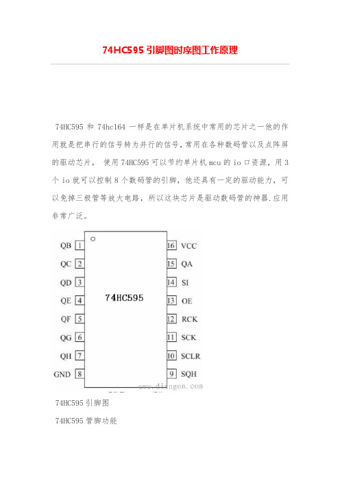
74HC595引脚图时序图工作原理74HC595和74hc164一样是在单片机系统中常用的芯片之一他的作用就是把串行的信号转为并行的信号,常用在各种数码管以及点阵屏的驱动芯片,使用74HC595可以节约单片机mcu的io口资源,用3个io就可以控制8个数码管的引脚,他还具有一定的驱动能力,可以免掉三极管等放大电路,所以这块芯片是驱动数码管的神器.应用非常广泛。
74HC595引脚图74HC595管脚功能下面我来介绍一下 74HC595工作原理:74HC595的数据端:QA--QH: 八位并行输出端,可以直接控制数码管的8个段。
QH’: 级联输出端。
我将它接下一个595的SI端。
SI: 串行数据输入端。
74hc595的控制端说明:/SCLR(10脚): 低电平时将移位寄存器的数据清零。
通常我将它接Vcc。
SCK(11脚):上升沿时数据寄存器的数据移位。
QA-->QB-->QC-->...-->QH;下降沿移位寄存器数据不变。
(脉冲宽度:5V时,大于几十纳秒就行了。
我通常都选微秒级)控制移位寄存器SCK 上升沿数据移位 SCK 下降沿数据保持RCK(12脚):上升沿时移位寄存器的数据进入存储寄存器,下降沿时存储寄存器数据不变。
通常我将RCK置为低电平,当移位结束后,在RCK端产生一个正脉冲(5V时,大于几十纳秒就行了。
我通常都选微秒级),更新显示数据。
控制存储寄存器RCK 上升沿移位寄存器的数据进入存储寄存器 RCK 下降沿存储寄存器数据不变/G(13脚): 高电平时禁止输出(高阻态)。
如果单片机的引脚不紧张,用一个引脚控制它,可以方便地产生闪烁和熄灭效果。
比通过数据端移位控制要省时省力。
注:74164和74595功能相仿,都是8位串行输入转并行输出移位寄存器。
74164的驱动电流(25mA)比74595(35mA)的要小,14脚封装,体积也小一些。
8位SARADC设计说明书

8位SAR ADC1关键名词解释文档中描述了12位ADC。
2功能概述图二。
1系统结构ADC子系统2包括一个8通道可配置模拟多路复用器(AMUX2)、一个可编程增益放大器(PGA2)和一个500ksps、8位分辨率逐次逼近型寄存器ADC,其中集成了一个跟踪保持电路。
AMUX2、PGA2和数据转换模式可由软件通过特殊功能寄存器进行配置。
仅当ADC2控制寄存器(ADC2_CN)的AD2EN位设为“1”时,ADC2子系统(8位ADC、采样保持和PGA)才使能。
当AD2EN位为“0”时,ADC2子系统处于低功耗关断模式。
ADC2有8个测量通道,由寄存器MUX_2SL选择通道。
PGA AMUX输出信号的放大系数由ADC2配置寄存器adc2 _ cf中的AMP2GN2-0决定,PGA可以通过软件编程为0.5、1、2、4,复位时的默认增益为0.5。
界面描述●3工作原理及电路性能分析3.1数字部分控制逻辑比较简单,主要总结控制逻辑的主要特点。
1)注意移位寄存器的第一位逻辑。
比较开始时,SAR的第一位设置为1,然后设置为0。
移位寄存器工作时只有一位是1,这就需要移位寄存器第一个触发器的输出Q端和输入D端有反馈逻辑。
2)当移位寄存器移位完成比较时,移位寄存器的下一位会发出完成信号通知数据寄存器,这样之前已经完成比较的位会一起输出。
同时,第一次转换后会通知采样信号,可以进行下一次采样。
3)双端差分输入和单端输入决定解码的最高位,通道配置寄存器提供通道配置信号,与ADC最高位形成决策逻辑。
4)移位寄存器和数据存储寄存器的复位信号也很重要,关系到ADC的启动。
3.2模拟部分3.2.1关于采样精度和采样时间SAR时钟频率为6MHz,所以比较器的延迟应为170ns,参考电压为 2.4v,比较器的分辨率为1/2 LSB = 4.6875mv,因此每级比较器的输出都有一个有限摆幅的反馈电路。
采样建立时间要求由下式给出:SA是建立精度,用LSB的分数表示(例如,0.25的建立精度相当于1/4 LSB)。
74HC595 74HCT595 8位串行输入、串行或并行输出的移位寄存器说明书

74HC595; 74HCT5958-bit serial-in, serial or parallel-out shift register with outputlatches; 3-stateRev. 9 — 28 February 2017Product data sheet 1General descriptionThe 74HC595; 74HCT595 is an 8-bit serial-in/serial or parallel-out shift register with astorage register and 3-state outputs. Both the shift and storage register have separateclocks. The device features a serial input (DS) and a serial output (Q7S) to enablecascading and an asynchronous reset MR input. A LOW on MR will reset the shiftregister. Data is shifted on the LOW-to-HIGH transitions of the SHCP input. The data inthe shift register is transferred to the storage register on a LOW-to-HIGH transition ofthe STCP input. If both clocks are connected together, the shift register will always beone clock pulse ahead of the storage register. Data in the storage register appears atthe output whenever the output enable input (OE) is LOW. A HIGH on OE causes theoutputs to assume a high-impedance OFF-state. Operation of the OE input does notaffect the state of the registers. Inputs include clamp diodes. This enables the use ofcurrent limiting resistors to interface inputs to voltages in excess of V CC.2Features and benefits•8-bit serial input•8-bit serial or parallel output•Storage register with 3-state outputs•Shift register with direct clear•100 MHz (typical) shift out frequency•Complies with JEDEC standard no. 7A•Input levels:–For 74HC595: CMOS level–For 74HCT595: TTL level•ESD protection:–HBM JESD22-A114F exceeds 2000 V–MM JESD22-A115-A exceeds 200 V•Multiple package options•Specified from -40 °C to +85 °C and from -40 °C to +125 °C3Applications•Serial-to-parallel data conversion•Remote control holding register8-bit serial-in, serial or parallel-out shift register with output latches; 3-state 4Ordering information5Functional diagram8-bit serial-in, serial or parallel-out shift register with output latches; 3-state8-bit serial-in, serial or parallel-out shift register with output latches; 3-state6Pinning information6.1Pinning74HC59574HCT595Q1V CC Q2Q0Q3DS Q4OE Q5STCP Q6SHCP Q7MR GNDQ7S001aao24212345678109121114131615Figure 5. Pin configuration for SO16, SSOP16 and TSSOP16001aao24374HC59574HCT595Q7MRQ6SHCP Q5STCP Q4OE Q3DS Q2Q0G N DQ 7S Q 1V C CTransparent top view71061151241331421589116terminal 1index areaGND (1)(1) This is not a supply pin. The substrate is attached to this pad using conductive die attach material. There is no electrical or mechanical requirement to solder this pad.However, if it is soldered, the solder land should remain floating or be connected to GND.Figure 6. Pin configuration for DHVQFN166.2Pin description8-bit serial-in, serial or parallel-out shift register with output latches; 3-state7Functional description[1][1]H = HIGH voltage state;L = LOW voltage state;↑ = LOW-to-HIGH transition;X = don’t care;NC = no change;Z = high-impedance OFF-state.8-bit serial-in, serial or parallel-out shift register with output latches; 3-state 8Limiting valuesTable 4. Limiting valuesIn accordance with the Absolute Maximum Rating System (IEC 60134). Voltages are referenced to GND (ground = 0 V).[1]For SO16 package: P tot derates linearly with 8 mW/K above 70 °C.[2]For SSOP16 and TSSOP16 packages: P tot derates linearly with 5.5 mW/K above 60 °C.[3]For DHVQFN16 package: P tot derates linearly with 4.5 mW/K above 60 °C.9Recommended operating conditions8-bit serial-in, serial or parallel-out shift register with output latches; 3-state 10Static characteristicsTable 6. Static characteristicsAt recommended operating conditions; voltages are referenced to GND (ground = 0 V).8-bit serial-in, serial or parallel-out shift register with output latches; 3-state8-bit serial-in, serial or parallel-out shift register with output latches; 3-state 11Dynamic characteristicsTable 7. Dynamic characteristicsVoltages are referenced to GND (ground = 0 V); for test circuit see Figure 13.8-bit serial-in, serial or parallel-out shift register with output latches; 3-state8-bit serial-in, serial or parallel-out shift register with output latches; 3-state[1]Typical values are measured at nominal supply voltage.[2]t pd is the same as t PHL and t PLH.[3]t en is the same as t PZL and t PZH.[4]t dis is the same as t PLZ and t PHZ.[5]C PD is used to determine the dynamic power dissipation (P D in μW).P D = C PD × V CC2 × f i + Σ(C L × V CC2 × f o) where:f i = input frequency in MHz;f o = output frequency in MHz;Σ(C L × V CC2 × f o) = sum of outputs;C L = output load capacitance in pF;V CC = supply voltage in V.[6]All 9 outputs switching.11.1Waveforms and test circuit8-bit serial-in, serial or parallel-out shift register with output latches; 3-state8-bit serial-in, serial or parallel-out shift register with output latches; 3-state8-bit serial-in, serial or parallel-out shift register with output latches; 3-state8-bit serial-in, serial or parallel-out shift register with output latches; 3-state 12Package outline8-bit serial-in, serial or parallel-out shift register with output latches; 3-state8-bit serial-in, serial or parallel-out shift register with output latches; 3-state8-bit serial-in, serial or parallel-out shift register with output latches; 3-state8-bit serial-in, serial or parallel-out shift register with output latches; 3-state 13Abbreviations14Revision history8-bit serial-in, serial or parallel-out shift register with output latches; 3-state 15Legal information15.1 Data sheet status[1]Please consult the most recently issued document before initiating or completing a design.[2]The term 'short data sheet' is explained in section "Definitions".[3]The product status of device(s) described in this document may have changed since this document was published and may differ in case of multipledevices. The latest product status information is available on the Internet at URL .15.2 DefinitionsDraft — The document is a draft version only. The content is still under internal review and subject to formal approval, which may result in modifications or additions. Nexperia does not give any representations or warranties as to the accuracy or completeness of information included herein and shall have no liability for the consequences of use of such information.Short data sheet — A short data sheet is an extract from a full data sheet with the same product type number(s) and title. A short data sheet is intended for quick reference only and should not be relied upon to contain detailed and full information. For detailed and full information see the relevant full data sheet, which is available on request via the local Nexperia sales office. In case of any inconsistency or conflict with the short data sheet, the full data sheet shall prevail.Product specification — The information and data provided in a Product data sheet shall define the specification of the product as agreed between Nexperia and its customer, unless Nexperia and customer have explicitly agreed otherwise in writing. In no event however, shall an agreement be valid in which the Nexperia product is deemed to offer functions and qualities beyond those described in the Product data sheet.15.3 DisclaimersLimited warranty and liability — Information in this document is believed to be accurate and reliable. However, Nexperia does not give any representations or warranties, expressed or implied, as to the accuracyor completeness of such information and shall have no liability for the consequences of use of such information. Nexperia takes no responsibility for the content in this document if provided by an information source outside of Nexperia. In no event shall Nexperia be liable for any indirect, incidental, punitive, special or consequential damages (including - without limitation -lost profits, lost savings, business interruption, costs related to the removal or replacement of any products or rework charges) whether or not such damages are based on tort (including negligence), warranty, breach of contract or any other legal theory. Notwithstanding any damages that customer might incur for any reason whatsoever, Nexperia's aggregate and cumulative liability towards customer for the products described herein shall be limited in accordance with the Terms and conditions of commercial sale of Nexperia.Right to make changes — Nexperia reserves the right to make changesto information published in this document, including without limitation specifications and product descriptions, at any time and without notice. This document supersedes and replaces all information supplied prior to the publication hereof.Suitability for use — Nexperia products are not designed, authorized or warranted to be suitable for use in life support, life-critical or safety-critical systems or equipment, nor in applications where failure or malfunctionof an Nexperia product can reasonably be expected to result in personal injury, death or severe property or environmental damage. Nexperia and its suppliers accept no liability for inclusion and/or use of Nexperia products in such equipment or applications and therefore such inclusion and/or use is at the customer’s own risk.Applications — Applications that are described herein for any of these products are for illustrative purposes only. Nexperia makes no representation or warranty that such applications will be suitable for the specified use without further testing or modification. Customers are responsible for the design and operation of their applications and products using Nexperia products, and Nexperia accepts no liability for any assistance with applications or customer product design. It is customer’s sole responsibility to determine whether the Nexperia product is suitable and fit for the customer’s applications and products planned, as well as for the planned application and use of customer’s third party customer(s). Customers should provide appropriate design and operating safeguards to minimize the risks associated with their applications and products. Nexperia does not accept any liability related to any default, damage, costs or problem which is based on any weakness or default in the customer’s applications or products, or the application or use by customer’s third party customer(s). Customer is responsible for doing all necessary testing for the customer’s applications and products using Nexperia products in order to avoid a default of the applications and the products or of the application or use by customer’s third party customer(s). Nexperia does not accept any liability in this respect.Limiting values — Stress above one or more limiting values (as defined in the Absolute Maximum Ratings System of IEC 60134) will cause permanent damage to the device. Limiting values are stress ratings only and (proper) operation of the device at these or any other conditions above thosegiven in the Recommended operating conditions section (if present) or the Characteristics sections of this document is not warranted. Constant or repeated exposure to limiting values will permanently and irreversibly affect the quality and reliability of the device.Terms and conditions of commercial sale — Nexperia products aresold subject to the general terms and conditions of commercial sale, as published at /profile/terms, unless otherwise agreed in a valid written individual agreement. In case an individual agreement is concluded only the terms and conditions of the respective agreement shall apply. Nexperia hereby expressly objects to applying the customer’s general terms and conditions with regard to the purchase of Nexperia products by customer.No offer to sell or license — Nothing in this document may be interpreted or construed as an offer to sell products that is open for acceptance orthe grant, conveyance or implication of any license under any copyrights, patents or other industrial or intellectual property rights.Export control — This document as well as the item(s) described herein may be subject to export control regulations. Export might require a prior authorization from competent authorities.8-bit serial-in, serial or parallel-out shift register with output latches; 3-state74HC_HCT595All information provided in this document is subject to legal disclaimers.© Nexperia B.V. 2017. All rights reserved.Product data sheet Rev. 9 — 28 February 201721 / 22Non-automotive qualified products — Unless this data sheet expressly states that this specific Nexperia product is automotive qualified, the product is not suitable for automotive use. It is neither qualified nor tested in accordance with automotive testing or application requirements. Nexperia accepts no liability for inclusion and/or use of non-automotive qualified products in automotive equipment or applications. In the event that customeruses the product for design-in and use in automotive applications toautomotive specifications and standards, customer (a) shall use the productwithout Nexperia's warranty of the product for such automotive applications,use and specifications, and (b) whenever customer uses the product forautomotive applications beyond Nexperia's specifications such use shall besolely at customer’s own risk, and (c) customer fully indemnifies Nexperiafor any liability, damages or failed product claims resulting from customer design and use of the product for automotive applications beyond Nexperia'sstandard warranty and Nexperia's product specifications.Translations — A non-English (translated) version of a document is for reference only. The English version shall prevail in case of any discrepancybetween the translated and English versions.15.4 Trademarks Notice: All referenced brands, product names, service names and trademarks are the property of their respective owners.8-bit serial-in, serial or parallel-out shift register with output latches; 3-statePlease be aware that important notices concerning this document and the product(s)described herein, have been included in section 'Legal information'.© Nexperia B.V. 2017.All rights reserved.For more information, please visit: Forsalesofficeaddresses,pleasesendanemailto:***************************Date of release: 28 February 2017Document identifier: 74HC_HCT595Contents1General description ............................................12Features and benefits .........................................13Applications .........................................................14Ordering information ..........................................25Functional diagram .............................................26Pinning information ............................................46.1Pinning ...............................................................46.2Pin description ...................................................47Functional description ........................................58Limiting values ....................................................69Recommended operating conditions ................610Static characteristics ..........................................711Dynamic characteristics .....................................911.1Waveforms and test circuit ..............................1112Package outline .................................................1513Abbreviations ....................................................1914Revision history ................................................1915Legal information . (20)Mouser ElectronicsAuthorized DistributorClick to View Pricing, Inventory, Delivery & Lifecycle Information:N experia:74HC595BQ,11574HC595D,11274HC595DB,11274HC595DB,11874HC595D,11874HC595N,11274HC595PW,11274HC595PW,11874HCT595BQ,11574HCT595D,11274HCT595DB,11274HCT595DB,118 74HCT595D,11874HCT595N,11274HCT595PW,11274HCT595PW,11874HC595PW/AUJ。
74HC595简介

74HC595简介DS:串行数据输入,接Arduino的某个数字I/O引脚。
Q0~Q7:8位并行数据输出,可以直接控制8个LED,或者是七段数码管的8个引脚。
Q7′:级联输出端,与下一个74HC595的DS相连,实现多个芯片之间的级联。
SH_CP:移位寄存器的时钟输入。
上升沿时移位寄存器中的数据依次移动一位,即Q0中的数据移到Q1中,Q1中的数据移到Q2中,依次类推;下降沿时移位寄存器中的数据保持不变。
ST_CP:存储寄存器的时钟输入。
上升沿时移位寄存器中的数据进入存储寄存器,下降沿时存储寄存器中的数据保持不变。
应用时通常将ST_CP 置为低点平,移位结束后再在ST_CP端产生一个正脉冲更新显示数据。
MR:重置(RESET),低电平时将移位寄存器中的数据清零,应用时通常将它直接连高电平(VCC)。
OE:输出允许,高电平时禁止输出(高阻态)。
引脚不紧张的情况下可以用Arduino的一个引脚来控制它,这样可以很方便地产生闪烁和熄灭的效果。
实际应用时可以将它直接连低电平(GND)。
在一些不是很复杂的应用中,可以将MR和OE分别接VCC和地,只对DS、SH_CP和ST_CP三个引脚进行相关控制。
二 C语言程序#include<reg52.h>#include<intrins.h>#include<lcd.h>#define uchar unsigned char#define uint unsigned intsbit DS = P2^7;sbit SH_CP = P3^0;sbit ST_CP = P3^1;sbit duanx = P3^2;uchar disp_buffer[4];uchar const table[10]={48,49,50,51,52,53,54,55,56,57}; //1到9的ASCII码uchar const table2[]={0x3f,0x06,0x5b,0x4f,0x66,0x6d,0x7d,0x07,0x7f,0x6f,0x77,0x7c,0x39,0x5e,0x79,0x71};//共阴void remove_data(uchar Re_data);void lcd_init(void);void main(void){uint j = 0;uchar *s1 = "VALUE:",temp_data,disp_data,a;write_str(s1,0,0);write_str(s2,0,1);while(1){duanx = 0;a = table2[j++];remove_data(a);delay(100);disp_data = a;temp_data = disp_data/1000; writlcd();write_char(table[temp_data],7,0); temp_data = disp_data%1000/100; writlcd();write_char(table[temp_data],8,0); temp_data = disp_data%100/10; writlcd();write_char(table[temp_data],9,0); temp_data = disp_data%10;write_char(table[temp_data],10,0); if(j == 9 )j = 0;}}void remove_data(uchar Re_data){uint i;for(i=8; i>0; i--){if(Re_data&0x80)//判断高位是否为1 DS = 1;elseDS = 0;SH_CP = 0;_nop_();_nop_();SH_CP = 1;Re_data <<=1; //Re_data左移一位ST_CP = 0;_nop_();_nop_();ST_CP = 1; //上升沿将数据送到输出锁存器_nop_();_nop_();ST_CP = 0;}void lcd_init(void){lcd_rest();lcd_winst(0x01);set_cur(1);其中程序中红色部分便是对74HC595进移位和锁存操作。
最新HC595芯片资料
H C595芯片资料HC 595芯片资料特点8位串行输入8位串行或并行输出存储状态寄存器,三种状态输出寄存器可以直接清除100MHz的移位频率输出能力并行输出,总线驱动串行输出;标准中等规模集成电路应用串行到并行的数据转换Remote control holding register.描述595是告诉的硅结构的CMOS器件,兼容低电压TTL电路,遵守JEDEC标准。
595是具有8位移位寄存器和一个存储器,三态输出功能。
移位寄存器和存储器是分别的时钟。
数据在SCHcp的上升沿输入,在STcp的上升沿进入的存储寄存器中去。
如果两个时钟连在一起,则移位寄存器总是比存储寄存器早一个脉冲。
移位寄存器有一个串行移位输入(Ds),和一个串行输出(Q<?xml:namespace prefix = st1 />7’),和一个异步的低电平复位,存储寄存器有一个并行8位的,具备三态的总线输出,当使能OE时(为低电平),存储寄存器的数据输出到总线。
参考数据符号参数条件 TYP 单位HC HCttPHL/tPLH 传输延时SHcp到Q7’STcp到QnMR到Q7’CL=15pFVcc=5V161714 212019 NsNsNsfmax STcp到SHcp最大时钟速度 10057 MHzCL 输入电容 Notes 1 3.5 3.5 pFCPD Power dissipation capacitance per package. Notes2 115 130 pFCPD决定动态的能耗,PD=CPD×VCC×f1+∑(CL×VCC2×f0)F1=输入频率,CL=输出电容 f0=输出频率(MHz) Vcc=电源电压引脚说明符号引脚描述Q0…Q7 15, 1, 7 并行数据输出GND 8 地Q7’ 9 串行数据输出MR 10 主复位(低电平)SHCP 11 移位寄存器时钟输入STCP 12 存储寄存器时钟输入OE 13 输出有效(低电平)DS 14 串行数据输入VCC 16 电源功能表输入输出功能SHCP STCP OE MR DS Q7’ Qn× × L ↓ × L NC MR为低电平时紧紧影响移位寄存器× ↑ L L × L L 空移位寄存器到输出寄存器× × H L × L Z 清空移位寄存器,并行输出为高阻状态↑ × L H H Q6’ NC 逻辑高电平移入移位寄存器状态0,包含所有的移位寄存器状态移入,例如,以前的状态6(内部Q6”)出现在串行输出位。
74hc165d驱动数码管工作原理 -回复
74hc165d驱动数码管工作原理-回复关于74hc165d驱动数码管的工作原理,需要从以下几个方面进行详细解释。
一、74hc165d芯片介绍74hc165d是一种快速CMOS逻辑阵列系列高性能的8位移位寄存器,能够同时读取多个输入信号,并将其存储在内部寄存器中。
它具有串行输入和并行输出的特点,适用于各种应用场合。
二、数码管基本原理数码管是一种常见的显示器件,采用LED(发光二极管)作为发光元素。
通过控制LED的亮灭状态,可以实现数字、字母和符号等字符的显示。
数码管通常由多个LED管组成,其中每个LED管都对应一个字符或数字。
三、74hc165d驱动数码管的连接方法1. 连接74hc165d与数码管:- 将74hc165d的并行输出引脚连接到相应的数码管段,共连接8个引脚,分别对应数码管的8个段。
- 将74hc165d的串行输出引脚连接到下一个74hc165d的串行输入引脚,形成级联连接。
2. 连接74hc165d与控制器:- 将74hc165d的时钟输入引脚(CLK)连接到控制器的时钟输出引脚(CLKOUT)。
- 将74hc165d的串行数据输入引脚(SER)连接到控制器的数据输出引脚(DATAOUT)。
- 将74hc165d的片选输入引脚(OE)连接到控制器的片选输出引脚(OEOUT)。
四、74hc165d驱动数码管的工作流程1. 初始化:- 控制器将时钟输出引脚置为低电平,将数据输出引脚置为高电平,将片选输出引脚置为低电平。
2. 数据读取:- 控制器将时钟输出引脚每次切换一个时钟脉冲,74hc165d每接收一个时钟脉冲,将一定数量的数据从串行输入引脚读取到内部寄存器中。
- 在每个时钟脉冲期间,数据由串行输入引脚传输到内部寄存器中。
- 当所有数据都传输到内部寄存器中后,74hc165d将所有数据都存储在内部寄存器中。
3. 数据输出:- 控制器将片选输出引脚置为高电平,使74hc165d的输出有效。
(完整word版)74HC595程序应用(附原理图)
74HC595芯片资料8位串行输入/输出或者并行输出移位寄存器,具有高阻关断状态。
三态。
特点8位串行输入8位串行或并行输出存储状态寄存器,三种状态输出寄存器可以直接清除100MHz的移位频率输出能力并行输出,总线驱动串行输出;标准中等规模集成电路应用串行到并行的数据转换Remote control holding register。
#include<reg51.h〉#include <intrins.h〉#define uchar unsigned char#define uint unsigned intsbit stcp1=P2^2;sbit ds1=P2^1;sbit shcp1=P2^0;sbit stcp2=P2^5;sbit ds2=P2^4;sbit shcp2=P2^3;uchar code DAT[11]={0x3f,0x06,0x5b,0x4f,0x66,0x6d,0x7d,0x07,0x7f,0x6f,0x00};//共阴数码管显示码uchar code tab[10]={0xbf,0x86,0xdb,0xcf,0xe6,0xed,0xfd,0x87,0xff,0xef};uchar code wei[9]={0xfe,0xfd,0xfb,0xf7,0xef,0xdf,0xbf,0x7f,0xff};void delay(uint ms){uint x,y;for(x=ms;x>0;x--)for(y=255;y>0;y--);}void QR0_5951(uchar num1){uchar j;for (j=0;j<8;j++){num1=num1〈<1 ;ds1=CY;shcp1=1;//上升沿发生移位// shcp1=0;}}void OUT_5951()//将移位寄存器内的数据锁存到输出寄存器并显示{stcp1=0;stcp1=1;//上升沿将数据送到输出锁存器stcp1=0;}void QR1_5952(uchar num2){uchar j;for (j=0;j<8;j++){num2=num2〈〈1 ;ds2=CY;shcp2=1;//上升沿发生移位// shcp2=0;}}void OUT_5952()//将移位寄存器内的数据锁存到输出寄存器并显示{stcp2=0;stcp2=1;//上升沿将数据送到输出锁存器stcp2=0;}void main(){uchar i;while(1){for(i=0;i<2;i++){QR0_5951(DAT[0]);OUT_5951();QR1_5952(wei[i]);OUT_5952();delay(1);}}}描述595是告诉的硅结构的CMOS器件,兼容低电压TTL电路,遵守JEDEC标准.595是具有8位移位寄存器和一个存储器,三态输出功能。
最详细的74HC595芯片使用方法介绍
最详细的74HC595芯片使用方法介绍2010-01-17 00:07:05 来源: 电子工程师论坛Arduino采用的ATmega168芯片带12个数字I/O管脚,其中每个都可以对一个数字量进行控制,从而实现类似于点亮一个发光二极管这样的功能。
在实际的工程应用里,有时我们可能会遇到需要对更多的数字量进行控制的场合,比如同时控制16个发光二极管,这时Arduino自带的数字I/O管脚就不够用了,必须进行相应的扩展。
其中一种可行的办法就是借助74HC595这样一个8位串入并出移位寄存器,这个芯片能够多个级连起来一起使用,因此理论上能够通过Arduino上有限的几个管脚(最少三个)产生任意多个的数字输出。
74HC595同数据相关的引脚可以分为三类:DS:串行数据输入,接Arduino的某个数字I/O引脚。
Q0~Q7:8位并行数据输出,可以直接控制8个LED,或者是七段数码管的8个引脚。
Q7′:级联输出端,与下一个74HC595的DS相连,实现多个芯片之间的级联。
74HC595同控制相关的引脚一共有四个:SH_CP:移位寄存器的时钟输入。
上升沿时移位寄存器中的数据依次移动一位,即Q0中的数据移到Q1中,Q1中的数据移到Q2中,依次类推;下降沿时移位寄存器中的数据保持不变。
ST_CP:存储寄存器的时钟输入。
上升沿时移位寄存器中的数据进入存储寄存器,下降沿时存储寄存器中的数据保持不变。
应用时通常将ST_CP置为低点平,移位结束后再在ST_CP端产生一个正脉冲更新显示数据。
MR:重置(RESET),低电平时将移位寄存器中的数据清零,应用时通常将它直接连高电平(VCC)。
OE:输出允许,高电平时禁止输出(高阻态)。
引脚不紧张的情况下可以用Arduino的一个引脚来控制它,这样可以很方便地产生闪烁和熄灭的效果。
实际应用时可以将它直接连低电平(GND)。
对于一个最简单的74HC595应用来讲,可以用Arduino的三个数字I/O端口分别控制DS、SH_CP和ST_CP,然后将MR和OE分别接VCC和地。
74HC164D中文资料 参数及应用
74HC164D中文资料参数SN54HC164,/SN74HC164是8位移位寄存器,当其中一个(或二个)选通串行输入端的低电平禁止进入新数据,并把第一个触发器在下一个时钟脉冲来后复位到低电平时,门控串行输入端(A 和B)可完全控制输入数据。
一个高电平输入后就使另一个输入端赋能,这个输入就决定了第一个触发器的状态。
虽然不管时钟处于高电平或低电平时,串行输入端的数据都可以被改变,但只有满足建立条件的信息才能被输入。
时钟控制发生在时钟输入由低电平到高电平的跃变上。
为了减小传输线效应,所有输入端均采用二极管钳位。
功能表:Inputs输入Outputs输出CLRCLK A B QA QB ...QHL X X X L L LH L X X QAQBQH0H↑H H H QAnQGnH↑L X L QAnQGnH↑X L L QAnQGnH=高电平(稳定态)L=低电平(稳定态)×=不定↑=从低电平转换到高电平QA0…QH0=在稳定态输入条件建立前QA…QH 的相应电平QAn…QHn=在最近的时钟输入条件(↑)建立前QA…QH 的相应电平,表示移位一位图1 逻辑图(正逻辑)图2 引脚图Absolute Maximum Ratings绝对最大额定值Supply voltage range, 电源电压范围VCC–0.5 V to 7V Input clamp current, 输入钳位电流IIK (VI < 0 or VI > VCC) (seeNote 1)±20 mA Output clamp current,输出钳位电流IOK (VO < 0 or VO > VCC) (seeNote 1)±20 mA Continuous output current,连续输出电流IO (VO = 0 to VCC)±25 mA Continuous current through 连续通过电流VCC or GND±50 mA封装热阻thermal impedance, θJA (see Note 2):D 封装86℃/W N 封装80℃/W NS 封装76℃/W PW 封装113℃/WStorage temperature range, Tstg储存温度范围–65℃ to 150℃DC SPECIFICATIONS直流电气规格表:符号Parameter 参数SN54HC164SN74HC164最小典型最大最小典型最大VCCSupply Voltage 电源电压256256图3 参数测量信息图4 typical clear, shift, and clear sequence典型清除、移位和清除时序应用电路:图5 LCD驱动电路图6 LED驱动电路74HC164中文资料参数时间:2016-06-15 来源:资料室作者:编号:颖展电子SN54HC164,/SN74HC164是8位移位寄存器,当其中一个(或二个)选通串行输入端的低电平禁止进入新数据,并把第一个触发器在下一个时钟脉冲来后复位到低电平时,门控串行输入端(A 和B)可完全控制输入数据。
74HC595同数据相关的引脚
74HC595同数据相关的引脚可以分为三类:DS:串行数据输入,接Arduino的某个数字I/O引脚。
Q0~Q7:8位并行数据输出,可以直接控制8个LED,或者是七段数码管的8个引脚。
Q7′:级联输出端,与下一个74HC595的DS相连,实现多个芯片之间的级联。
74HC595同控制相关的引脚一共有四个:SH_CP:移位寄存器的时钟输入。
上升沿时移位寄存器中的数据依次移动一位,即Q0中的数据移到Q1中,Q1中的数据移到Q2中,依次类推;下降沿时移位寄存器中的数据保持不变。
ST_CP:存储寄存器的时钟输入。
上升沿时移位寄存器中的数据进入存储寄存器,下降沿时存储寄存器中的数据保持不变。
应用时通常将ST_CP置为低点平,移位结束后再在ST_CP端产生一个正脉冲更新显示数据。
MR:重置(RESET),低电平时将移位寄存器中的数据清零,应用时通常将它直接连高电平(VCC)。
OE:输出允许,高电平时禁止输出(高阻态)。
引脚不紧张的情况下可以用Arduino的一个引脚来控制它,这样可以很方便地产生闪烁和熄灭的效果。
实际应用时可以将它直接连低电平(GND)。
对于一个最简单的74HC595应用来讲,可以用Arduino的三个数字I/O端口分别控制DS、SH_CP和ST_CP,然后将MR 和OE分别接VCC和地。
下面是利用74HC595来控制8个LED的原理图:One Response to “74HC595串入并出8位移位寄存器”i3dx Says:December 26th, 2007 at 9:09 pm订正:Arduino 带有 0-7 8-13 14-19 共三组,20个数字IO口。
只是14-19常用于模拟输入端0-5口使用,但是基本数字io功能仍然保留。
Arduino mini 另有20 21两个数字io 可使用。
单片机与74LS595(8位输出锁存移位寄存器)的使用方法74LS595的数据端:QA--QH: 八位并行输出端,可以直接控制数码管的8个段。
- 1、下载文档前请自行甄别文档内容的完整性,平台不提供额外的编辑、内容补充、找答案等附加服务。
- 2、"仅部分预览"的文档,不可在线预览部分如存在完整性等问题,可反馈申请退款(可完整预览的文档不适用该条件!)。
- 3、如文档侵犯您的权益,请联系客服反馈,我们会尽快为您处理(人工客服工作时间:9:00-18:30)。
8位移位寄存器原理详解
寄存器的基本概念
在计算机系统中,寄存器是一种用于暂时存储数据的硬件设备。
它可以在短时间内快速读取和写入数据,并且可以进行各种操作,如移位、逻辑运算等。
寄存器通常是由触发器构成的,触发器是一种能够存储一个比特位(0或1)的电子设备。
移位寄存器的基本原理
移位寄存器是一种特殊类型的寄存器,它可以将数据按照一定规则进行移动。
8位
移位寄存器就是指具有8个触发器的移位寄存器。
1. 数据输入
8位移位寄存器具有一个数据输入端,用于输入待操作的数据。
这个输入端可以接
受一个8位二进制数作为输入。
2. 数据输出
8位移位寄存器具有一个数据输出端,用于输出经过操作后得到的结果。
这个输出
端也是一个8位二进制数。
3. 移动方向控制
8位移位寄存器有两个控制信号:Shift Left和Shift Right,分别用于控制向左移动和向右移动。
当Shift Left信号为高电平时,寄存器中的数据将向左移动一位;当Shift Right信号为高电平时,寄存器中的数据将向右移动一位。
4. 移位操作
当移位方向控制信号确定后,8位移位寄存器会根据这个信号将其中的数据进行移动。
具体的移动方式有以下几种:
•向左循环移动(Shift Left Circular):最左边的比特位被移到最右边,其余比特位按顺序向左移动。
•向右循环移动(Shift Right Circular):最右边的比特位被移到最左边,其余比特位按顺序向右移动。
•向左非循环移动(Shift Left Non-Circular):所有比特位都向左移动一位,最左边的比特位丢失。
•向右非循环移动(Shift Right Non-Circular):所有比特位都向右移动一位,最右边的比特位丢失。
5. 控制时钟
8位移位寄存器通常还有一个控制时钟信号。
这个时钟信号用来同步触发器,在时
钟脉冲到达时执行相应操作。
每当时钟脉冲到达时,寄存器会根据当前控制信号进行相应的操作。
移位寄存器应用举例
1. 数据缓存
移位寄存器可以用作数据缓存,将数据从输入端输入到寄存器中,并根据需要进行移位操作。
这样可以在一段时间内保持数据的稳定,方便后续处理。
2. 数据传输
移位寄存器还可以用于数据的传输。
通过将数据输入到寄存器中,并根据需要进行移位操作,可以将数据从一个地方传输到另一个地方。
3. 数据压缩与解压缩
在某些应用中,需要对数据进行压缩和解压缩操作。
移位寄存器可以通过循环移动或非循环移动来实现这一功能。
4. 密码加密与解密
在密码学中,移位寄存器也有广泛的应用。
通过对输入的数据进行特定的移位操作,可以实现简单的密码加密和解密算法。
总结
8位移位寄存器是一种具有8个触发器的特殊类型寄存器,它可以将输入的数据按
照不同的规则进行移动。
通过控制信号和控制时钟,我们可以实现各种不同方向和方式的移位操作。
这使得8位移位寄存器在各种应用场景下都有广泛的应用,如数据缓存、数据传输、数据压缩与解压缩以及密码加密与解密等。
希望通过本文的详细解释,您对8位移位寄存器的基本原理有了更清晰、易于理解的认识。