恒流源模块TD9910
DS9135数据手册

DS9135
产品特点
●低启动电流(<8uA)
●集成650V功率MOSFET
●PFM模式原边反馈控制
●内置负载调节补偿
●恒压/恒流工作
●输出短路保护
●FB引脚开路/短路保护
●2ms软启动
●Vcc的过电压保护(OVP)
●内部过温保护(OTP)
●DIP-7封装,外部所需很少器件产品选型功能描述
DS9135是一款PFM模式用于反激式变换器的高性能原边反馈控制器,最大限度的减少了元器件的数量,并采用了微小的DIP-7封装。
这使它成为低成本应用的理想设计。
并且提供了低启动电流、绿色模式省电操作,VCC过压保护、FB引脚异常情况感应,防止电路因异常状态而损坏。
应用领域
●手机充电器
●低功率AC/DC适配器
产品型号封装Rdson
DS9135L DIP-7 3.6Ω
DS9135K DIP-7 2.0Ω
DS9135E DIP-7 1.5Ω
DS9135C DIP-7 1.0Ω
典型应用信息
高精度CC/CV原边控制开关电源芯片
DS9135
Tel: +86 186****2042
1。
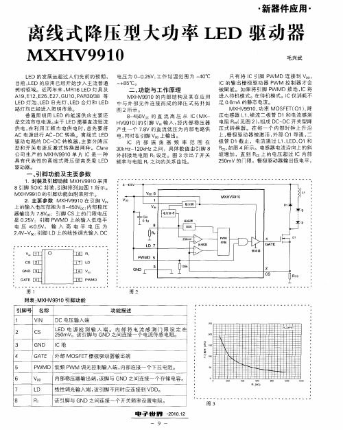
离线式降压型大功率LED驱动器MXHV9910
VN I
C S
—L _ I
j卜 II l j
—
l j I,一 1_圭 L I I砰 J 1 L jr
I I f }一 丰 # 厂 I- }i I } 【
十 — + r + I 斗十 L
f
3
GN D
一
毛 兴 武
只 有 将 I 引脚 P MD 连 接 到 V 。 C W D, I C的输 出栅 极驱动器 P M 控 制器 才会 W 被 赋 能 。 如 果 将 引 脚 P MD 接 地 , W l C将 二 、 能与 工作原 理 功 C仅 MX V 9 0 的 内 部 结 构 及 其 在 应 用 进 入待 机 模 式 。在待 机 模 式 。I 消耗 不 H 91 mA 的 静态 电流 。 中 与 外 部 元 件 连 接 而 成 的 降 压 式 拓 扑 如 足 06
电压 为 O 02 V; 作 结 温 范 围 为 一 OC ~ .5 工 4 。
+ 5 C。 8 。
~
MX V 9 0 功 率 MOS E ( H 9 1、 F T Q1)降 、 1续 1和 电流 感 测 8 4 0 u 的 直 流 高 压 从 I MX 压 电 感器 L 、 流 二极 管 D ~ 5 Vc C( — c ( )组 C D H 91 ) V 9 0 的引脚 V 输 入 , 内部 稳压 器 电阻 RS见 图 2 , 成 D — C开 关型 降 。 经
l C地
4 5
6
G 丁 外部 MOS E AE F T栅极驱动器输出端 P WMD 低频 P M 调光控制输入端 , W 内部连接 一个下拉 电阻。
VD D 内部 稳 压 器 输 出端 , 该脚 与 G ND之 间 连 接一 个 存 储 电容 。
康佳电视进入总线方法

康佳彩电总线进入方法详解1.康佳彩电18大系列K/N系列、SK系列、S系列、SE系列、SA系列、A系列、C系列、E系列、F系列、ST系列、TA8880CN机芯(画中画系列)、倍频机芯、W机芯(背投系列)、T系列(数字高清)、I系列(数字高清)、M、FM系列(数字高清)、FG、FT系列(数字高清)、MV系列(数字高清)。
2.1 K/N系列2.1.1彩电配置一览表主要IC:超级芯片TDA9380或TDA93832.1.2总线调整方法机型:TDA9380掩膜后的型号为CKP1402SA,代表机型有:P2162K、T2168K、T2168N、P2179K、T2176N、T2176K等;TDA9383掩膜后的型号为CKP1403SA,代表机型有:T3468K、P3460K、P2960K、P2961K、P2962K、P2962K1、P2998K、T2975K、T2968K、T2976K、T2968N、P2562K、P2579K、T2568K、T2568N按MENU(菜单)键调出菜单显示(注:菜单显示时间为10s),在菜单未消失前连续按回看键5次便可进入工厂调整菜单。
按MENU键可依次选择菜单1到菜单4。
选中需调整的菜单后,可用节目+/-键选择需调整的项目(选中后变为红色);用音量控制键调节选中项目的参数值,直至符合要求为止。
当所有调试完成后,再按一次回看键即可退出总线调整模式,回到正常收看状态。
2.1.3总线故障故障现象:接收PAL-I制信号时,伴音音轻且有杂音。
检修提示:进入维修状态,在维修菜单5内设有伴音制式设定项目,其中SOUND FILTER 即是伴音滤波器选择设定项目,数据为"00"时,选择内部SIF电路处理全制式伴音信号;"01"时,选择外部电路处理6.5MHz伴音信号;"02"时,选择外部电路处理6.0MHz伴音信号;"03"时,选择外部电路处理全制式伴音信号。
复位IC,电源管理IC系列,替代型号及参数

复位IC,电源管理IC系列,替代型号及参数复位ICPJ809 series(2.63/2.93/3.08/4.0/4.38/4.63V)PJ810 series(2.63/2.93/3.08/4.0/4.38/4.63V)PJ705/706/707/708/813EL Driver ICPJ6540C(驱动面积20-40 CM2)PJ6540S(驱动面积20-40 CM2)PJ6540TS(驱动面积20-40 CM2)PJ6543S/TS(驱动面积50-100 CM2)高电压检测ICPJ6101C/NXXXMR series(1.1-6.0V,每隔0.1有型号)LCD Driver ICSC1904(驱动点数19X4)SC1621(驱动点数32X4)SC1621(驱动点数32X4)SC1622(驱动点数32X8)SC1622(驱动点数32X8)SL4808(驱动点数48X8)SC1626(驱动点数48X16)SC1626(驱动点数48X16)SC6523(驱动点数52X3)PJ8566S(驱动点数32X4)小功率AB类音频放大ICPJ4890(1W)PJ4990(1.25W)PJ4871(1.5W)PJ4871(PP)(底部带散热片,1.5W)TDA2822(12V,2X1W)PJ2822(12V,2X1W)TDA2822(9V,2X1W)PJ2822(9V,2X1W)TDA2822(6V,2X1W)LM386中功率AB类音频放大ICPJ4888(2X2.1W,带3D混响功能和立体声耳机功能)PJ4818(2X2.2W,带立体声耳机功能)PJ4088(2X2.2W,带立体声耳机功能)PJ4863MTE(2X2.2W)PJ4863S/P(2X2.2W)CSC4863S(2X2.2W)TEA2025(12V,2X2.5W)TEA2025(9V,2X2.5W)PJ4836(2X2W,带重低音)PJ4836(2X2W,带重低音)TDA7496(2X2W)D1517P(2X4W)TA8227(2X3W)KA2206(2X2.3W)APA2068((2X2.6W,带音量控制,底部带散热片)大功率AB类音频放大ICTDA2030A(18W)LM1875T/L(20W)TDA7265(2X25W)YD7377(2X30W或4X6W)D类音频放大ICPJ2005(1.4W,单声道,D类音频放大)PJ2010(1.3W,单声道,D类音频放大)TPA2012D2(2X1.4W,立体声,D类音频放大)PJ2012(2X1.5W,立体声,D类音频放大)AX2012(2X1.4W,立体声,D类音频放大)PJ8008(2X1.5W,立体声,D类音频放大)耳机音频放大ICPJ4800(2X290mW,立体声耳机放大IC)PJ4808(2X105mW,立体声耳机放大IC)PJ4809(2X105mW,高电平关断,立体声耳机放大IC)PJ8608(2X105mW,立体声耳机放大IC)PJ4880(2X250mW,立体声耳机放大IC)PJ7000(2X40mW,立体声耳机放大IC)LM4853M(2X300mW立体声耳机放大或1.5W单声道耳机放大 IC)全差分AB类音频放大ICPJ4898(全差分,1W)PJA6211(全差分,1.25W)PJA6203(全差分,1.25W)音量音质处理ICCSC2313(三组立体声输入音质处理IC,6V-10V.)CSC2314(四组立体声输入音质处理IC,6V-10V.)D2322(6通道AV前置控制IC,5-12V.)D2323(6通道音响输入选择IC,4.5-12V.)CSC2256(双声道音量控制IC,2.5V-12V.)PT2258(六声道音量控制IC,5V-10V.)M62429(双声道音量控制IC,5V.)TC9153(音量控制IC,4.5-12V.)混响处理ICCD2399单片调频调幅收音ICCD9088(单片电调谐调频收音IC)CD1191(单片调频调幅收音IC)TA2003(单片调频调幅收音IC)YT2111(单片调频调幅立体声收音IC)YD2149(单片调频调幅收音IC/3V工作)并联白灯背光ICPJ7110(并3路白灯,每路20mA)PJ7111(并4路白灯,每路20mA)PJ5920(并3路白灯,每路20mA)PJ5921(并4路白灯,每路20mA)PJ9300(并4路白灯,每路20mA)PJ3200(并5路白灯,每路20mA)PJ2133(并4路白灯,每路可达30mA)PJ60230(并5路白灯,每路可达30mA)PJ9364(并4路白灯,每路可达20mA)PJ9362(并4路白灯,每路可达30mA)PJ9360(并4路白灯,每路可达30mA)PJ3114(并6路白灯,每路20mA)霍尔ICPJ90248S/TPJ177A/B/CPJ1881S/TPJ732S/TPJ211A/B/CTPJ41S/TPJ49ETPJ40APJ5881PJ3144RS232接口ICMAX232锂电保护ICPJ5426AB(4.3V过充保护电压)PJ5426BB(4.28V过充保护电压)PJ2188(4.3V过充保护电压,内置MOS的2合1锂电保护IC)锂电保护板所用MOS管PJ9926SPJ9926TPJ8205T(新版样品)PJ8205MR(新版样品)PJ5N20VPJ8810TPJ8810MRPJ8822TPJ8822MRPJ8818TPJ8818MRPJ8820MRPJ8208PJ6968PJ8209MR单节锂电充电ICPJ4054MR(800mA)PJ4054DR(800mA)PJ4054PR(1A)PJ4056MR(800mA,带双灯指示功能)PJ4060C(250mA,双灯指示功能,其中一个灯为七彩灯指示) PJ4060D(250mA,双灯指示功能)PJ4050S(500mA)PJ2051S(1A)PJ4100(1A)VM7205M/S(1A,须外接场效应管)PJ9501A/B(1A,须外接场效应管,B:4.2V,A:4.1V,一般推B版的)单节锂电/镍氢电池/铅酸电池线性充电ICPJ4062S(500mA,4.2V充满,充电电压可调,也可充镍氢/铅酸电池) PJ4066(1A,4.2V充满,充电电压可调,也可充镍氢/铅酸电池)单节磷酸铁锂电/镍氢电池/铅酸电池线性充电ICPJ4058S(500mA,3.6V充满,充电电压可调,也可充镍氢/铅酸电池) PJ4059(1A,3.6V充满,充电电压可调,也可充镍氢/铅酸电池)开关电源绿色模式PWM控制ICPJ6848M/PPJ6850M/P/SPJ6853M/PPJ6842M/P/SPJ6860(15W)PJ2530A(5W)PJ2603P(6W,内置700V三极管)PJ2604P(6W-8W,内置700V三极管)PJ2605S(3.8W-4.5W,内置700V三极管)PJ2607P(18W,须外加高压功率三极管)PJ8022P(20W以下,内置700VMOS管,输入电压9-38V,耐压50V) PJ8012P(13W以下,内置730VMOS管,输入电压10-39V,耐压50V) PJ1203(5-120W,输入电压耐压16V)I2C实时时钟/日历ICPJ8563S/P/T/MPJ1302S/PAM/FM 频率显示驱动ICSC3610SC3610D马达驱动ICD5898(PDVD 含双路DC-DC 4通道马达驱动IC)D5668(DVD 5通道马达驱动IC)D5868(DVD 5通道马达驱动IC)D5888(DVD 5通道马达驱动IC)D5954(DVD/PDVD/Car DVD/CD机 4通道马达驱动IC)D9258(DVD/PDVD/Car DVD/CD机 4通道马达驱动IC)D9259(DVD/PDVD/Car DVD/CD机 5通道马达驱动IC)YT5901(CD机4通道马达驱动IC)PJ6651AN6650(马达稳速IC)PJ7010R(马达正反转控制驱动IC,1-2A驱动电流)PJ9110(马达正反转控制驱动IC,0.8A驱动电流)PJ9120(马达正反转控制驱动IC,3A驱动电流,须加三级管扩流) PJ9130(直流马达正反转及加速驱动IC,3A驱动电流,须加三级管扩流)锁相环ICAT9256AT9257LC72131电阻式触摸屏控制ICPJ2046PJ2003电容式触摸按键ICTF601(6键输入,工作电压2.5-5.5V)TF401(4键输入,工作电压2.5-5.5V)TF201(2键输入,工作电压2.5-5.5V)TF101(1键输入,工作电压2.5-5.5V)通用运算放大器ICLM324S(四运放/32V)LM324P(四运放/32V)LM324S(四运放/18V)LM324P(四运放/18V)LM358S/P(双运放)JRC4558(双运放)低压运算放大器ICPJ3414(双运放)PJ4510(双运放)PJ2107(单运放)低压低功耗运算放大器ICS324(四运放)S358(双运放)低噪声低失真运算放大器ICPJ4580(双运放)PJ4560(双运放)PJ2568(双运放)大电流运算放大器ICPJ4556(双运放)高带宽高转换速率运算放大器ICPJ2137(双运放)低漂移高精度运算放大器ICOP07(单运放)中频接收ICMC3361通话免提ICMC34018PJ34118PJ34119通话话音网络ICTEA1062/A(A:低电平静噪)压扩电路ICTA31101F(语音压扩电路IC)SL5015(压扩电路IC)SL5020(低压压扩电路IC)DC DC变换ICPJ34063A(1.5A)MC34063B(0.8A)PJ34063(0.8A)三端可调正电源稳压ICLM317L(100mA)LM317T(1.5A)电流型PWM控制ICKA3842S/PKA3843S/P固定频率PWM控制ICKA7500PKA7500STL494PTL494SPJ9741电压比较器ICLM339S(4电压比较器)LM339P(4电压比较器)LM393S/P(双电压比较器)LED显示屏驱动ICPJ62726SS/SO/SP(16位恒流LED驱动IC,每路输出4-90mA) PJ6024(16位恒流LED驱动IC,每路输出3-45mA)LED数码管显示驱动IC(移位寄存器IC)PJ74HC164PJ74HC164PJ74HC595门电路ICPJ74HC244(8路3态缓冲驱动IC)PJ74HC04(六反相器IC)PJ74HC14(六反相施密特触发器IC)SC74HC245(总线驱动双向三态门电路IC)SC74HC138(3-8译码器IC)SC74HC27(四总线收发器IC)SC74HC373(八D锁存器IC)SC74HC393(双4位二进制计数器IC)TFT-LCD 时序控制ICPVI1004DTFT-LCD 信号处理ICD3031LCD视频切换开关ICPI5V330定时器ICNE555立体声D/A转换ICPJ433416位音频D/A转换ICPJ8211CCFL冷光阴极灯控制ICPJ3105恒流恒压控制ICPJ1051MR2A DDR 电源ICPJ9174七路达林顿驱动器阵列ULN2003(七路达林顿驱动器阵列,最大驱动电流可达500MA) ULN2003(七路达林顿驱动器阵列,最大驱动电流可达500MA)模拟开关ICPJ3157(高速单刀双掷模拟开关IC)电源开关ICPJ9701双卡控制ICPJ6188(SPI接口双卡控制IC)4路ESD保护ICPJ3205MRSOT23SOT23SOP8/DIP8 DiceSOP8TSSOP8SOP8/TSSOP8 SOT23DiceDiceSSOP48DiceQFP64DiceDiceQFP100QFP64/LQFP64 LQFP44 MSOP8SMD9(=CSP9) SOP8/DIP8 SOP8(PP)DIP8SOP8DIP8SOP8SOP8/DIP8 SOP8/DIP8 QFN24QFN24QFN16 TSSOP20(PP) SOP16/DIP16 SOP16WSOP16/DIP16 SOP16/DIP16 TSSOP28(PP) HSOP28DIP20/SOP20 DIP18FDIP12SOP16-PPHZIP5TO-220B-5/TO-220-5HZIP11ZIP15QFN8/MSOP8SMD9(=CSP9)/QFN8(=DFN8)QFN20/WCSP16QFN20/WCSP16SOP16WTSSOP20SOP8MSOP8MSOP8SOP8SOP8/DIP8SSOP10MSOP10MSOP10/SMD9(=CSP9)MSOP8/SMD9(=CSP9)SMD9(=CSP9)/QFN8(=DFN8)/MSOP8 SOP28/DIP28SOP28/DIP28SOP28/DIP28SOP28/DIP28SOP16/SOP16WDIP20SOP8/DIP8DIP16DIP16/SOP16SOP16SOP28DIP16/SSOP16SDIP24/SSOP24SDIP24/SSOP24SOT-26MSOP8MSOP8SOT-26SOT-26QFN16QFN16QFN16QFN16QFN16QFN16SOT-23/TO-92 SOT-23/TO-92 SOT-23/TO-92 SOT-23/TO-92 TO-94SOT-23/TO-92 TO-92TO-92/SOT-23 TO-92/SOT-23 TO-92/SOT-23SOP16/DIP16SOT-26SOT-26 TSSOP8SOP8TSOP8TSSOP8 TSSOP6(SOT26) TSSOP8 TSSOP8 TSSOP6(SOT26) TSSOP8 TSSOP6(SOT26) TSSOP8 TSSOP6(SOT26) TSSOP6(SOT26) TSSOP8 TSSOP8 TSSOP6(SOT26) SOT-25DFN10SOT-89-5SOT-26SOT-26SOT-26SOP8SOP8DFN10MSOP8/SOP8MSOP8SOP8DFN10SOP8DFN10SOT-26/DIP8SOT-26/DIP8/SOP8SOT-26/DIP8SOT-26/DIP8/SOP8TO-92TO-92DIP8DIP8SOP8DIP8DIP8DIP8SOP8SOP8/DIP8/TSSOP8/MSOP8 SOP8/DIP8DiceCOB(SOP36)HSOP34HSOP28HSOP28HSOP28HSOP28HSOP28HSOP28QFP44TO-126DIP8SOP8/DIP8SOP8/DIP8SOP8/DIP8DIP16SOP16/DIP16 SOP20/DIP20 DIP22/MFP22QFN16/TSSOP16 TSSOP16SSOP20SOP14SOP8SOP8SOP14DIP14SOP14DIP14SOP8/DIP8 SOP8/DIP8 SOP8/DIP8 SOP8/DIP8 SOT-25/SOP8SOP14/DIP14 SOP8/DIP8 SOP8/DIP8 SOP8/DIP8 SOP8/DIP8SOP8/DIP8SOP8/DIP8SOP8/DIP8SOP16/DIP16SOP28/DIP28 SOP28/DIP28 SOP8/DIP8DIP16SOP16SOP20/DIP20SOP14/DIP14SOP8/DIP8SOP8/DIP8DIP8TO-92TO-220SOP8/DIP8SOP8/DIP8DIP16SOP16DIP16SOP16SSOP16/SOP16SOP14DIP14SOP8/DIP8SSOP24/SOP24/SDIP24 SSOP24/SOP24/QFN24 DIP14(插片)SOP14(贴片)SOP16SOP20SOP14SOP14SOP20SOP16SOP14DIP20DIP14QFP64QFP48SSOP16SOP8/DIP8SOP8/DIP8 SOP8 SSOP20 SOT-26 SOP8DIP16 SOP16 SOT-26 SOT-25 QFN20 SOT-26MAX809/IMP809 seriesMAX810/IMP810 seriesMAX705/706/707/708/813/IMP705/706/707/708/813 series 兼容SM8141兼容SM8141兼容SM8141兼容SM8142XC6101FC(FN)/XC6101CC(CN) seriesHT1621/SL3204HT1621/SL3204HT1622/SL3208HT1622/SL3208HT1623HT1626/SL4816HT1626/SL4816PT6523/SC75823PCF8566LM4890/LM4889/APA0711/NCP2890/PT2366LM4890/LM4889/LM4990/NCP2990LM4871LM4871TDA2822/KA2209TDA2822/KA2209TDA2822/KA2209TDA2822/KA2209TDA2822/KA2209LM386LM4888LM4818/SN4188SN4088/LPA4911LM4863MTELM4863LM4863TEA2025TEA2025LM4836LM4836TDA1517APA2068/G1450TPA2005TPA2010/NCP2820/TS4962/EUA2010/A7013/LM4670/1/3/5/APA2010/PT2333 LM4674TPA2012TPA2012TMPA2155PSTDA1308/LM4800/PT2308/APA4800LM4808LM4809LM4808LM4880/HT82V735FAN7000LM4898/LM4894TPA6211/TPA6204TPA6203PT2313/SC7313PT2314/SC7314PT2322PT2323PT2256PT2258M62429TC9153PT2399TDA9088/TDA7088/TDA1088CXA1191TA2003TA2111TA2149AMC7110AMC7111G5920G5921RT9300LTC3200/AAT3110/RT9361/AAT1501/AIC1848CP2133/FAN5616TPS60230RT9364RT9362RT9360/SC604/CAT3406/PAM2701AAT3114MLX90248/A180/A3212/TLE4913/EW6672ATC177/ATS177US1881EW732/EW512/DN6851FTC211/FTS211SS41/SS400/US1881UA/UGN3175/77UA/UGN3075/77UA/A3132/33/34UA/HAL105/115/125 SS49E/AH41ESS40AUS5881A3144/UGN3140/2/UGS3140/2/A3141/2/3DW01+/CS213/R5426/DW01DW01+/CS213/R5426/DW01兼容CR6002CEM9926/APM9926/AP9926/AO8822/AO8810CEM9926/APM9926/AP9926/AO8822/AO8810CEM8205/APM8205/AP8205/AO8205CEM8205/APM8205/AP8205/AO82055N20VAO8810AO8810AO8822AO8822AO8818AO8818AO8820AO8208APM6968AO8209LTC4054ES5/MCP73831-2(SOT-25)/MCP73832-2(SOT-25)/OCP8020LTC4054ES5/MCP73831-2/MCP73832-2/OCP8020LTC4054ES5/MCP73831-2/MCP73832-2)/OCP8020LTC4054ES5/MCP73831-2(SOT-25)/MCP73832-2(SOT-25)/OCP8020VA7205/VA7202RT9501SG6848/LD7550/OB2262SG6850/LD7550/OB2262/SG5701/SG5848SG6851/LD7535/OB2263/SG6848/SG6849/SG5701/SG5848/LD7550/OB2262/OB2278/OB2279 SG6841/SG6842/LD7552/OB2268/OB2269ACT30/AP3700ACT30/AP3700THX202THX203THX208THX201Viper22Viper12NCP1203PCF8563/PT7C4337DS1302/HT1380/HT1381AM5898AM5668AM5868AM5888BA5954KA9258KA9259BA5901AN6651LG7010LG9110LG9130TC9256/PT9256TC9257/PT9257TSC2046/ADS7846/MT6301/AK4182/ADS7843 TSC2003LM4558/JRC4558NJM3414NJM4510NJM2107SGM324/LMV324SGM358/LMV358NJM4580NJM4560NJM2568NJM4556NJM2137OP07DBL5018/SL5018SC34018MC34118/SC34118MC34119/SC34119SL5015SL5020MC34063AMC34063BLM3842LM3843TL494TL494BA9741/TL1451/SP9741/A1250/AP2001/FP1451 TB62726/MBI5026MBI502474HC16474HC16474HC59574HC24474HC0474HC1474HC24574HC13874HC2774HC37374HC393IR3Y31CS4334PT8211/TDA1311/HT82V731BIT3105TSM1051/SL71051/BD6550G/NJM2336 RT9174ULN2003ULN2003SGM3157RT9701MT6302MAX3205/SRV05-4。
电源电路模块
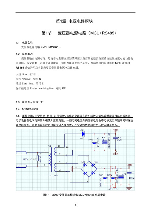
第1章电源电路模块第1节变压器电源电路(MCU+RS485)1.1 电路名称变压器电源电路(MCU+RS485)。
1.2 电路概述变压器输出电源电路,是将市电利用变压器的降压以及后续的整流稳压输出低压直流电的功能电源电路。
本文针对公司静止式电能表、预付费电能表等产品中,普遍使用的输出提供MCU计量和RS485通信的两路负载需要的变压器电源电路作介绍。
火线Line,缩写L零线Neutral,缩写N地线Earth line,缩写E保护接地线Protect earthing line,缩写PE1.3 电路图及原理分析1.4 MYN23-751K1.5 压敏电阻:主要用途:防雷,过压保护。
如电力变压器在进户端放入氧化锌避雷器可以有效防雷,电子设备在电网电源输入端放入压敏电阻,一但电网电压升高压敏电阻会不可恢复击穿短路同时保险丝也将断开,从而有效的放止过电压进入线路板。
在空调线线路板应用压敏电阻最为多。
图1-1230V变压器单相提供MCU+RS485电源电路1.5.1 变压器电源电路(MCU+RS485)一般原理如图1-1所示,变压器电源电路基本功能是将电网中的交流电,通过变压器的电磁转换从副极线圈输出低压交流电。
如图(编号6和7)的副边低压交流电经过整流桥堆的整流操作输出一个脉动电压,这个脉动电压通过(如C1类)的电解电容器的滤波,在DV1稳压二极管的钳位作用下转换成了可以用于LDO等低压稳压器件操作的直流电。
另一组(编号9、10)副边低压交流电通过二极管的半波整流操作输出一个脉动电压,之后通过C3的滤波和DV2的稳压二极管钳位作用输出一个可用于低压稳压器件操作的直流电。
然而,如C1电解电容器在整个电能表的供电模块中还扮演着掉电瞬间数据存储提供能量的重要角色,所以选取的时候需谨慎,详细请看1.3.2.5。
图1-1中红色虚框中的DV3稳压二极管是在客户需要380V过压的时候加上(或将DV1换成额定功率>2W的稳压二极管),没有过压要求的可以去掉,详见1.3.2.4。
稳压模块
EZELAND 输入特性输入电压范围(lnput voltage range) 4.75VDC-5.25VDC 11.40VDC-12.60VDC 14.25VDC-15.75VDC 22.80VDC-25.20VDC 45.60VDC-50.40VDC输出特性输出电压精度(voltage accuracy) 标称输出电压±3%负载效应(Load regulation) 0%至100%负载变化时±1.0%(最大值)源效应(Line regulation) 输入电压从低端至高端变化时±1.0%(最大值) 纹波及噪声(Ripple and noise) 50mVpk-pk(最大值)温度系数(Temperature coefficient) ±0.10%/℃(最大值)一般特性效率(Efficiency)见产品选型表隔离电压(lsolation voltage) 输入至输出(1分钟漏电流<0. 5mA)500VDC开关频率(Switching frequency)150KHz最小无故障间隔时间(MTBF) 200000小时环境特性工作温度(Operatlng ambient)-25℃至+85℃最大壳温(Max Case temperature)+90℃存储温度(Storage temperature)-40℃至+120℃相对湿度(Relative density)10%至90%SR01系列产品型号输入电压范围(V)标称输出电压(V)标称输出电流(mA )纹波及噪声(mVp-p) 典型效应(%) V out1 V out2 lout1 lout2 out1 out2SR5S5/100A 4.75-5.25 5 100 50 40 SR5S12/100A 4.75-5.25 12 100 50 52 SR5S15/100A 4.75-5.25 15 100 50 52 SR5S24/50A 4.75-5.25 24 50 50 52 SR12S5/100A 11.40-12.60 5 100 50 40 SR12S12/100A 11.40-12.60 12 100 50 52 SR12S15/100A 11.40-12.60 15 100 50 52SR12S24/50A 11.40-12.60 24 50 50 52 SR15S5/100A 14.25-15.75 5 100 50 40 SR15S12/100A 14.25-15.75 12 100 50 52 SR15S15/100A 14.25-15.75 15 100 50 52 SR15S24/50A 14.25-15.75 24 50 50 52 SR24S5/100A 22.80-25.20 5 100 50 40 SR24S12/100A 22.80-25.20 12 100 50 52 SR24S15/100A 22.80-25.20 15 100 50 52 SR24S24/50A 22.80-25.20 24 50 50 52 SR5D5/100A 4.75-5.25 +5 -5 100 100 50 50 45 SR5D12/50A 4.75-5.25 +12 -12 50 50 50 50 52 SR5D15/50A 4.75-5.25 +15 -15 50 50 50 50 52 SR5D24/20A 4.75-5.25 +24 -24 20 20 50 50 52 SR12D5/100A 11.40-12.60 +5 -5 100 100 50 50 45 SR12D12/50A 11.40-12.60 +12 -12 50 50 50 50 52 SR12D15/50A 11.40-12.60 +15 -15 50 50 50 50 52 SR12D24/20A 11.40-12.60 +24 -24 20 20 50 50 52 SR15D5/100A 14.25-15.75 +5 -5 100 100 50 50 45 SR15D12/50A 14.25-15.75 +12 -12 50 50 50 50 52 SR15D15/50A 14.25-15.75 +15 -15 50 50 50 50 52 SR15D24/20A 14.25-15.75 +24 -24 20 20 50 50 52 SR24D5/100A 22.80-25.20 +5 -5 100 100 50 50 45 SR24D12/50A 22.80-25.20 +12 -12 50 50 50 50 52 SR24D15/50A 22.80-25.20 +15 -15 50 50 50 50 52 SR24D24/20A 22.80-25.20 +24 -24 20 20 50 50 52SR03系列产品型号输入电压范围(V)标称输出电压(V)标称输出电流(mA)纹波及噪声(mVp-p)典型效应(%) V out1 V out2 V out3 lout1 lout2 lout3 out1 out2 out3SR5S5/200A 4-75-5.25 5 200 50 40 SR5S5/200B 4.75-5.25 5 200 50 50 SR5S5/500B 4.75-5.25 5 500 50 55SR5S12/250B 4.75-5.25 12 250 50 60 SR5S15/200B 4.75-5.25 15 200 50 60 SR5S24/125B 4.75-5.25 24 125 50 60 SR12S5/200A 11.40-12.60 5 200 50 40 SR12S5/500B 11.40-12.60 5 500 50 55 SR12S12/250B 11.40-12.60 12 250 50 60 SR12S15/200B 11.40-12.60 15 200 50 60 SR12S24/125B 11.40-12.60 24 125 50 60 SR24S5/200A 22.80-25.20 5 200 50 40 SR24S5/500B 22.80-25.20 5 500 50 55 SR24S12/250B 22.80-25.20 12 250 50 60 SR24S15/200B 22.80-25.20 15 200 50 60 SR24S24/125B 22.80-25.20 24 125 50 60 SR48S5/500B 45.60-50.40 5 500 50 55 SR48S12/250B 45.60-50.40 12 250 50 60 SR48S15/200B 45.60-50.40 15 200 50 60 SR48S24/125B 45.60-50.40 24 125 50 60 SR5D12/100A 4.75-5.25 +12 -12 100 100 50 50 52 SR5D12/100B 4.75-5.25 +12 -12 100 100 50 50 60 SR5D15/100A 4.75-5.25 +15 -15 100 100 50 50 52 SR5D15/100B 4.75-5.25 +15 -15 100 100 50 50 60 SR5D24/60B 4.75-5.25 +24 -24 60 60 50 50 60 SR12D12/100A 11.40-12.60 +12 -12 100 100 50 50 52 SR12D12/100B 11.40-12.60 +12 -12 100 100 50 50 60 SR12D15/100A 11.40-12.60 +15 -15 100 100 50 50 52 SR12D15/100B 11.40-12.60 +15 -15 100 100 50 50 60 SR12D24/60B 11.40-12.60 +24 -24 60 60 50 50 60 SR15D12/100A 14.25-15.75 +12 -12 100 100 50 50 52 SR15D15/100A 14.25-15.75 +15 -15 100 100 50 50 52 SR24D12/100A 22.80-25.20 +12 -12 100 100 50 50 52 SR24D12/100B 22.80-25.20 +12 -12 100 100 50 50 60 SR24D15/100A 22.80-25.20 +15 -15 100 100 50 50 52 SR24D15/100B 22.80-25.20 +15 -15 100 100 50 50 60SR24D24/60B 22.80-25.20 +24 -24 60 60 50 50 60 SR48D12/100B 45.60-50.40 +12 -12 100 100 50 50 60 SR48D15/100B 45.60-50.40 +15 -15 100 100 50 50 60 SR48D24/60B 45.60-50.40 +24 -24 60 60 50 50 60 SR5D12S5B 4.75-5.25 +12 -12 +5 100 100 100 50 50 50 64 SR5D15S5B 4.75-5.25 +15 -15 +5 100 100 100 50 50 50 64 SR12D12S5B 11.40-12.60 +12 -12 +5 100 100 100 50 50 50 64 SR12D15S5B 11.40-12.60 +15 -15 +5 100 100 100 50 50 50 64 SR24D12S5B 22.80-25.20 +12 -12 +5 100 100 100 50 50 50 64 SR24D15S5B 22.80-25.20 +15 -15 +5 100 100 100 50 50 50 64SR05系列产品型号输入电压范围(V)标称输出电压(mA)标称输出电流(mA)纹波及噪声(mVp-p)典型效应(%) V out1 V out2 lout1 lout2 out1 out2SR5S5/1000B 4.75-5.25 5 1000 50 65 SR5S5/1000C 4.75-5.25 5 1000 50 60 SR5S12/400C 4.75-5.25 12 400 50 64 SR5S15/300C 4.75-5.25 15 300 50 64 SR5S24/200C 4.75-5.25 24 200 50 64 SR12S5/1000B 11.40-12.60 5 1000 50 65 SR12S5/1000C 11.40-12.60 5 1000 50 60 SR12S12/400C 11.40-12.60 12 400 50 64 SR12S15/300C 11.40-12.60 15 300 50 64 SR12S24/200C 11.40-12.60 24 200 50 64 SR24S5/1000B 22.80-25.20 5 1000 50 65 SR24S5/1000C 22.80-25.20 5 1000 50 60 SR24S12/400C 22.80-25.20 12 400 50 64 SR24S15/300C 22.80-25.20 15 300 50 64 SR24S24/200C 22.80-25.20 24 200 50 64 SR48S5/1000C 45.60-50.40 5 1000 50 60 SR48S12/400C 45.60-50.40 12 400 50 64 SR48S15/300C 45.60-50.40 15 300 50 64 SR48S24/200C 45.60-50.40 24 200 50 64 SR5D5/500C 4.75-5.25 +5 -5 500 500 50 50 60SR5D12/150C 4.75-5.25 +12 -12 150 150 50 50 64 SR5D15/150C 4.75-5.25 +15 -15 150 150 50 50 64 SR5D24/100C 4.75-5.25 +24 -24 100 100 50 50 64 SR12D5/500C 11.40-12.60 +5 -5 500 500 50 50 60 SR12D12/150C 11.40-12.60 +12 -12 150 150 50 50 64 SR12D15/150C 11.40-12.60 +15 -15 150 150 50 50 64 SR12D24/100C 11.40-12.60 +24 -24 100 100 50 50 64 SR24D5/500C 22.80-25.20 +5 -5 500 500 50 50 60 SR24D12/150C 22.80-25.20 +12 -12 150 150 50 50 64 SR24D15/150C 22.80-25.20 +15 -15 150 150 50 50 64 SR24D24/100C 22.80-25.20 +24 -24 100 100 50 50 64 SR48D5/500C 45.60-50.40 +5 -5 500 500 50 50 60 SR48D12/150C 45.60-50.40 +12 -12 150 150 50 50 64 SR48D15/150C 45.60-50.40 +15 -15 150 150 50 50 64 SR48D24/100C 45.60-50.40 +24 -24 100 100 50 50 64模块电源用途:电力、医疗、通讯、电子仪器仪表、电力、自动化、智能楼宇、安防、电力机车、继电保护等天津泽沥电子。
电磁兼容(EMC)设计参考电路
1000pF/2KV FBMA-11-160808-601A10T
1 2 3.3V-Earth
L5
1000pF
C5
C6
1000pF
C1 1000pF
L3
C4 100nF
C3
100nF
C13 1000pF/2KV C14 1000pF/2KV
A
备注: 1、C2、C9、C10、C11 为预设计,根据实际的情况增加,一般不需要增加; 2、C13、C14为预设计,根据实际的情况增加或调整; 3.如防雷等级需要打空接(4、5、7、8)pin,可接上D5做防护。 4.此方案相比中心抽头的方案有了明显的差摸保护。如果要测试绝缘阻抗,请与工程师确认具体的方案。 5.如果4、5、7、8 PIN 不需要测试的话,这部分的器件可以不加
5
3
2
1
千兆网口EMC设计标准电路
D
C1 100nF
1 TCT1 TD1+ TD1-
U1
MCT1 MX1+ MX124 23 22 MX1+ MX1MX1+ MX1MX2+ MX3+ MX3MX2MX4+ MX41 2 3 4 5 6 7 8 MX1+ MX1MX2+ MX3+ MX3MX2MX4+ MX49
MCT3 MX3+ MX3-
18 17 16 MX3+ MX3-
TVS3
BV03C
330R R5 link_o
C4 100nF
10 11 12
TCT4 TD4+ TD4-
MCT4 MX4+ MX4-
15 14 13 MX4+ MX4-
IXYS IC Division MXHV9910 LED驱动器说明书
INTEGRATED C IRCUITS D IVISIONMXHV9910Off-Line, High BrightnessLED DriverFeatures•8V DC to 450V DC Input Voltage Range •>90% Efficiency•Drives Multiple LEDs in Series/Parallel Combinations•Regulated LED Drive Current•Linear or PWM Brightness Control•Resistor-Programmable Oscillator Frequency •RoHS CompliantApplications•Flat-Panel Display RGB Backlighting •Signage and Decorative LED Lighting •DC/DC or AC/DC LED Driver ApplicationsDescriptionThe MXHV9910 is a low-cost, high-brightness (HB) LED driver manufactured using IXYS IC Division’s high-voltage BCDMOS on SOI process. This driver has internal circuitry that allows it to operate from a universal AC line or from 8V DC to 450V DC . This highly versatile input operating voltage enables this IC to be used in a broad range of HB LED applications.The driver features a fixed-frequency, peak-current control method, which provides an ideal solution for driving multiple LEDs in series and in parallel. In addition, LED dimming can be implemented by applying a small DC voltage to the LD pin, or by applying a low-frequency digital PWM signal to the PWMD pin.The MXHV9910 is available in a standard 8-lead SOIC package and a thermally enhanced 8-lead SOIC package with an Exposed Thermal Pad (EP)Ordering InformationMXHV9910 Block DiagramPart DescriptionMXHV9910B SOIC-8 (100/T ube)MXHV9910BTR SOIC-8 T ape & Reel (2000/Reel)MXHV9910BE SOIC-8 EP (100/T ube)With Exposed Thermal PadMXHV9910BETRSOIC-8 EP T ape & Reel (2000/Reel)With Exposed Thermal Pad1Specifications . . . . . . . . . . . . . . . . . . . . . . . . . . . . . . . . . . . . . . . . . . . . . . . . . . . . . . . . . . . . . . . . . . . . . . . . . . . . . . . . . . . . . . . . . . . 31.1Package Pinout . . . . . . . . . . . . . . . . . . . . . . . . . . . . . . . . . . . . . . . . . . . . . . . . . . . . . . . . . . . . . . . . . . . . . . . . . . . . . . . . . . . . . . 31.2Pin Description . . . . . . . . . . . . . . . . . . . . . . . . . . . . . . . . . . . . . . . . . . . . . . . . . . . . . . . . . . . . . . . . . . . . . . . . . . . . . . . . . . . . . . . 31.3Absolute Maximum Ratings . . . . . . . . . . . . . . . . . . . . . . . . . . . . . . . . . . . . . . . . . . . . . . . . . . . . . . . . . . . . . . . . . . . . . . . . . . . . . 31.4Recommended Operating Conditions . . . . . . . . . . . . . . . . . . . . . . . . . . . . . . . . . . . . . . . . . . . . . . . . . . . . . . . . . . . . . . . . . . . . . 41.5Electrical Characteristics . . . . . . . . . . . . . . . . . . . . . . . . . . . . . . . . . . . . . . . . . . . . . . . . . . . . . . . . . . . . . . . . . . . . . . . . . . . . . . . 41.6Thermal Characteristics . . . . . . . . . . . . . . . . . . . . . . . . . . . . . . . . . . . . . . . . . . . . . . . . . . . . . . . . . . . . . . . . . . . . . . . . . . . . . . . . 4 2Functional Description . . . . . . . . . . . . . . . . . . . . . . . . . . . . . . . . . . . . . . . . . . . . . . . . . . . . . . . . . . . . . . . . . . . . . . . . . . . . . . . . . . . . 52.1Overview . . . . . . . . . . . . . . . . . . . . . . . . . . . . . . . . . . . . . . . . . . . . . . . . . . . . . . . . . . . . . . . . . . . . . . . . . . . . . . . . . . . . . . . . . . . 52.2LED Driver Theory of Operation . . . . . . . . . . . . . . . . . . . . . . . . . . . . . . . . . . . . . . . . . . . . . . . . . . . . . . . . . . . . . . . . . . . . . . . . . 52.2.1Input Voltage Regulator . . . . . . . . . . . . . . . . . . . . . . . . . . . . . . . . . . . . . . . . . . . . . . . . . . . . . . . . . . . . . . . . . . . . . . . . . 62.2.2Current Sense Resistor . . . . . . . . . . . . . . . . . . . . . . . . . . . . . . . . . . . . . . . . . . . . . . . . . . . . . . . . . . . . . . . . . . . . . . . . . . 62.2.3Current Sense Blanking . . . . . . . . . . . . . . . . . . . . . . . . . . . . . . . . . . . . . . . . . . . . . . . . . . . . . . . . . . . . . . . . . . . . . . . . . 72.2.4Enable/Disable . . . . . . . . . . . . . . . . . . . . . . . . . . . . . . . . . . . . . . . . . . . . . . . . . . . . . . . . . . . . . . . . . . . . . . . . . . . . . . . . 72.2.5Oscillator . . . . . . . . . . . . . . . . . . . . . . . . . . . . . . . . . . . . . . . . . . . . . . . . . . . . . . . . . . . . . . . . . . . . . . . . . . . . . . . . . . . . . 72.2.6Inductor Design . . . . . . . . . . . . . . . . . . . . . . . . . . . . . . . . . . . . . . . . . . . . . . . . . . . . . . . . . . . . . . . . . . . . . . . . . . . . . . . . 72.2.7Gate Output Drive . . . . . . . . . . . . . . . . . . . . . . . . . . . . . . . . . . . . . . . . . . . . . . . . . . . . . . . . . . . . . . . . . . . . . . . . . . . . . . 82.2.8Linear Dimming . . . . . . . . . . . . . . . . . . . . . . . . . . . . . . . . . . . . . . . . . . . . . . . . . . . . . . . . . . . . . . . . . . . . . . . . . . . . . . . . 82.2.9PWM Dimming . . . . . . . . . . . . . . . . . . . . . . . . . . . . . . . . . . . . . . . . . . . . . . . . . . . . . . . . . . . . . . . . . . . . . . . . . . . . . . . . 82.2.10Combination Linear and PWM Dimming . . . . . . . . . . . . . . . . . . . . . . . . . . . . . . . . . . . . . . . . . . . . . . . . . . . . . . . . . . . . . 9 3Manufacturing Information . . . . . . . . . . . . . . . . . . . . . . . . . . . . . . . . . . . . . . . . . . . . . . . . . . . . . . . . . . . . . . . . . . . . . . . . . . . . . . . . 103.1Moisture Sensitivity . . . . . . . . . . . . . . . . . . . . . . . . . . . . . . . . . . . . . . . . . . . . . . . . . . . . . . . . . . . . . . . . . . . . . . . . . . . . . . . . . . 103.2ESD Sensitivity . . . . . . . . . . . . . . . . . . . . . . . . . . . . . . . . . . . . . . . . . . . . . . . . . . . . . . . . . . . . . . . . . . . . . . . . . . . . . . . . . . . . . 103.3Reflow Profile . . . . . . . . . . . . . . . . . . . . . . . . . . . . . . . . . . . . . . . . . . . . . . . . . . . . . . . . . . . . . . . . . . . . . . . . . . . . . . . . . . . . . . . 103.4Board Wash . . . . . . . . . . . . . . . . . . . . . . . . . . . . . . . . . . . . . . . . . . . . . . . . . . . . . . . . . . . . . . . . . . . . . . . . . . . . . . . . . . . . . . . . 103.5Mechanical Dimensions . . . . . . . . . . . . . . . . . . . . . . . . . . . . . . . . . . . . . . . . . . . . . . . . . . . . . . . . . . . . . . . . . . . . . . . . . . . . . . . 113.5.1MXHV9910B: SOIC-8 . . . . . . . . . . . . . . . . . . . . . . . . . . . . . . . . . . . . . . . . . . . . . . . . . . . . . . . . . . . . . . . . . . . . . . . . . . 113.5.2MXHV9910BE: SOIC-8 With Exposed Thermal Pad . . . . . . . . . . . . . . . . . . . . . . . . . . . . . . . . . . . . . . . . . . . . . . . . . . 113.6Packaging Information . . . . . . . . . . . . . . . . . . . . . . . . . . . . . . . . . . . . . . . . . . . . . . . . . . . . . . . . . . . . . . . . . . . . . . . . . . . . . . . . 123.6.1Tape & Reel Information for both 8-Pin Packages . . . . . . . . . . . . . . . . . . . . . . . . . . . . . . . . . . . . . . . . . . . . . . . . . . . . 121. Specifications1.1 Package Pinout1.2Pin Description1.3Absolute Maximum RatingsElectrical absolute maximum ratings are at 25°C.Absolute maximum ratings are stress ratings. Stresses in excess of these ratings can cause permanent damage to the device. Functional operation of the device at conditions beyond those indicated in the operational sections of this data sheet is not implied.Pin#Name1V I N Input voltage2CS LED Current Sense input. Internal current sense threshold is set at 250mV . The external sense resistor sets the maximum LED current.3GND Device Ground4GA TE External MOSFET gate driver output5PWMD Low-frequency PWM dimming control input with internal pull-down resistor.6V DD Regulated supply voltage output. Requires a storage capacitor to GND. Can be overdriven by external voltage applied to V DD .7LD Linear Dimming. Apply a voltage less than V CS(high) to dim the LED(s).8R TResistor to GND sets the oscillator/primary PWM frequency.EP -Electrical and thermal conductive pad on the bottom of the MXHV9910BE. Connect this pad to ground, and provide sufficient thermal coupling to remove heat from the package.ParameterSymbol Maximum Unit Input Voltage to GNDV I N-0.5 to +460V Inputs & Outputs Voltage to GND CS, LD, PWMD, GA TE-0.3 to V DD +0.3V V DD , Externally Applied V DD.EXT 15V Power DissipationSOIC-8 With Thermal T ab P D 2.5W SOIC-8 W/O Thermal T ab 0.975W Maximum Junction T emperature T Jmax 150°C Operating T emperature T A -40 to +85°C Junction T emperature (Operating)T J -40 to +150°C Storage T emperatureT STG-55 to +150°C1.4Recommended Operating Conditions1.5Electrical CharacteristicsUnless otherwise specified, all electrical specifications are provided for T A =25︒C.1.6Thermal Characteristics1Use of a four-layer PCB can improve thermal dissipation (reference EIA/JEDEC JESD51-5).Symbol Minimum Nominal Maximum Unit Input Voltage Range V I N 8-450V DC PWMD Frequency f PWMD -500-Hz Operating T emperatureT A-40-+85°CSymbol MinimumTypical Maximum Unit InputInput DC Voltage RangeDC Input VoltageV IN 8-450V DC Shut-Down Mode Supply Current PWMD to GND, V I N =15 to 450V I INSD -0.30.6mA Maximum Voltage to V DD Pin External Voltage applied to V DD PinV DDmax--12VRegulatorInternal Voltage Regulator V I N =15V to 450V ,I DD(ext)=0,GA TE Output=OpenV DD 7.27.88.4V DC V DD Current Available for External Circuitry -I DD(ext)--2mA V DD Load Regulation V I N =15V , I L =1mA ∆V DD --200mV PWM DimmingPWMD Input Low Voltage V I N =8V to 450V V E N (low)--0.5V PWMD Input High Voltage V I N =8V to 450V V E N (high) 2.4--PWMD Pull-Down Resistance V I N =12V , V PWMD =V DDR E N70115165k ΩCurrent Sense Comparator Current Sense (CS) Input Current CS Low CS=0V I IL --45-90μA CS HighCS=V DDI IH -0±15Current Sense Threshold Voltage -40°C < T A < 85°C V CS(high)200-280mV Current Sense Blanking Interval R T =400k Ωt BLA N K -400-ns Delay from CS T rip to Gate Low R T =400k Ωt DELAY-300-ns OscillatorOscillator Frequency (Gate Driver)R T =400k Ωf S 516477kHz Gate DriverGate High Output Voltage I OUT = -10mA V GATE (hi)V DD -0.3--V Gate Low Output Voltage I OUT =10mA V GATE (lo)-0.030.3Gate Output Rise Time C GATE =500pF t RISE -16-nsGate Output Fall TimeC GATE =500pFt FALL-7-PackageSymbol MinimumTypical MaximumUnit Thermal Resistance, Junction-to-AmbientSOIC-8 With Thermal Pad (BE) 1R θJA-50-°C/WSOIC-8 W/O Thermal Pad (B)-128-2. Functional Description Figure1Typical Application Circuit2.1 OverviewThe MXHV9910 is a high-efficiency, low cost, off-line LED driver designed using IXYS IC Division's state of the art BCDMOS on SOI process. The driver can operate from a DC supply voltage between 8 to450V DC . The versatile input supply voltage range enables this driver to be used in a broad range of applications such as flat panel display RGB backlighting, signage, decorative LED lighting, and incandescent lamp replacement.The MXHV9910 IC is configured in a buck converter topology, which is a perfect choice for off-line and DC applications driving multiple LEDs in series or parallel. This method provides excellent efficiency and enables a buck switcher design using a minimum number of external components. An external current sense resistor sets the peak current to the LED string. In addition, LED dimming can be implemented by either applying a DC control voltage to the LD pin, or by applying a low frequency, pulse-width modulated digital signal to the PWMD pin (typically 500 Hz).2.2 LED Driver Theory of OperationThe gate driver pulse width mode (PWM) control circuit is enabled by connecting the PWMD pin to the V DD pin. When enabled, the rising edge of each internal clock turns on the gate driver and the external power MOSFET, causing the inductor current to ramp up the voltage across the current sense resistor located at the CS pin. When the rising voltage at the current sense, CS, pin exceeds V CS(high), the internally set threshold, the gate drive signal goes low and turns off the external power MOSFET. T urning the power MOSFET off causes the inductor current to decay until the next rising edge of the clock, and the process repeats.The peak current threshold is set by comparing the voltage developed across the R SE N SE resistor to the internal threshold, V CS(high). This default threshold can be overridden externally by applying a voltage less than V CS(high) to the LD pin. The lower of these two thresholds limits the peak current in the inductorA soft-start function can be implemented by slowly ramping up the DC voltage at the LD pin from 0mV to a level greater than 250mV. Figure2 shows a typical recommended soft-start circuit design.Figure2Soft-Start RC NetworkFigure 3MXHV9910 Waveforms (From Application Circuit in Figure 6)2.2.1Input Voltage RegulatorThe MXHV9910 has an internal voltage regulator that can work with input voltages ranging from 12V DC to 450 V DC . When the input voltage applied at the V I N pin is greater than 12V DC , the internal voltage regulator regulates this voltage down to a typical 7.8V . The V DD pin is the internal regulator output pin and must be bypassed by a low ESR capacitor, typically 0.1μF, to provide a low impedance path for high frequency switching noise.The MXHV9910 driver does not require the bulky start-up resistors typically needed for off-linecontrollers. An internal voltage regulator provides sufficient voltage and current to power the internal IC circuits. This voltage is also available at the V DD pin, and can be used as bias voltage for external circuitry.The internal voltage regulator can by bypassed by applying an external DC voltage to the V DD pin that is slightly higher than the internal regulator’s maximum output voltage. This feature reduces power dissipation of the integrated circuit and is more suitable in isolated applications where an auxiliary transformer winding could be used to supply V DD .The total input current drawn by the V I N pin is equal to the integrated circuit quiescent current, which is 0.6mA maximum, plus the gate driver current. The gate driver current is dependant on the switching frequency and the gate charge of the external power MOSFET .The following equation can be used to approximate the V I N input current:Where Q GATE is the total gate charge of the external power MOSFET , and f S is the switching oscillator frequency.2.2.2Current Sense ResistorThe peak LED current is set by an external current sense resistor connected from the CS pin to ground. The value of the current sense resistor is calculated based on the desired average LED current, the current sense threshold, and the inductor ripple current. The inductor is typically selected to be large enough to keep the ripple current (the peak-to-peak difference in the inductor current waveform) to less than 30% of the average LED current. Factoring in this ripple current requirement, the current sense resistor can be determined by:Where:•V csth = nominal current sense threshold = 0.25V •r iout = inductor ripple = 0.3•I LED = average LED currentThe power dissipation rating of the sense resistor can be found with the following formula:CH1:50mA/div F S 65kHz CH2:CH3:5mV/div x 10Time Scale: 5μs/divMax 77mA10V/div I IN 0.6mA Q GATE f S ⨯()+≈R sense V csth10.5r iout ⨯()+[]I LED⨯-------------------------------------------------------------=P I LED 2R sense⨯=It is a good practice to select a power rating that is at least twice the calculated value. This will give proper margins, and make the design more reliable.2.2.3Current Sense BlankingThe MXHV9910 has an internal current-sense blanking circuit. When the power MOSFET is turned on, the external inductor can cause an undesired spike at the current sense pin, CS, initiating a premature termination of the gate pulse. T o avoid this condition, a typical 400ns internal leading edge blanking time is implemented. This internal feature eliminates the need for external RC filtering, thus simplifying the design. During the current sense blanking time, the current limit comparator is disabled, preventing the gate-drive circuit from terminating the gate-drive signal.2.2.4Enable/DisableConnecting the PWMD pin to V DD enables the gate driver. Connecting PWMD to G N D disables the gate driver and sets the device into the shut-down mode. In the shut-down mode, the gate output drive is disabled while all other functions remain active. The maximum quiescent current in the shut-down mode is 0.6mA.2.2.5OscillatorThe MXHV9910 operates in a constant frequency mode. Setting the oscillator frequency is achieved by connecting an external resistor between R T and G N D. In general, switching frequency selection is based on the inductor size, controller power dissipation, and the input filter capacitor.The typical off-line LED driver switching frequency, f S, is between 30kHz and 120kHz. This operating range gives designers a reasonable compromise between switching losses and inductor size. The internal RC oscillator has a frequency accuracy of ±20%. Figure4 shows the R T resistor selection for the desired f S.Figure4Resistor Selection2.2.6Inductor DesignThe inductor value is determined based on LED ripple current, maximum on-time, the forward voltage drop of all LEDs in a string at the desired current, and the minimum input voltage, which is based on design requirements. The maximum on-time is determined by the duty cycle and switching frequency. The maximum duty cycle is given by:Where:•V LEDstring is the LED string voltage at desired average LED current.•V in is the minimum input voltage to V I NThe maximum duty cycle must be restricted to less than 50% in order to prevent sub-harmonic oscillations and open loop instability.The converter maximum O N-time is given by:Where f s is the switching frequency of the internal oscillator.D maxV LEDstringV in-------------------------=t ONmaxD maxf s------------=The inductor value for the given ripple is:The inductor peak current rating is given by:2.2.7Gate Output DriveThe MXHV9910 uses an internal gate drive circuit to turn on and off an external power MOSFET . The gate driver can drive a variety of MOSFETs. For a typical off-line application, the total MOSFET gate charge will be less than 25nC.2.2.8Linear DimmingA linear dimming function can be implemented by applying a DC control voltage to the LD pin. By varying this voltage, the user can adjust the current level in the LEDs, which in turn will increase or decrease the light intensity. The control voltage to the LD pin can be generated from an external voltage divider network from V DD . This function is useful if the user requires a LED current at a particular level and there is no exact R sense value available. N ote that applying a voltage higher than the current sense threshold voltage at the LD pin will not change the output current due to the fixed threshold setting. When the LD pin is not used, it should be connected to V DD .Figure 5Typical Linear Dimming Application Circuit2.2.9PWM DimmingPulse width modulation dimming can be implemented by driving the PWMD pin with a low frequency square wave signal in the range of a few hundred Hertz. The PWMD signal controls the LED brightness by gating the PWM gate driver output pin GA TE.The signal can be generated by a microcontroller or a pulse generator with a duty cycle proportional to the amount of desired light output. When PWMD is low, gate drive is off; when PWMD is high, gate drive is enabled.L minV in V LEDstring –()t ONmax ⨯r iout I LED⨯--------------------------------------------------------------------=I Lmax I LED 10.5r iout ⨯()+[]⨯=Figure6Buck Driver for PWM Dimming Application Circuit Array2.2.10Combination Linear and PWM DimmingA combination of linear and PWM dimming techniquescan be used to achieve a large dimming ratio.Note: The output current will not go to zero if the LDpin is pulled to G N D because the minimum gate driveron-time is equal to the current sense blanking interval.T o achieve zero LED current, the PWMD pin should beused.3. Manufacturing Information3.1 Moisture SensitivityAll plastic encapsulated semiconductor packages are susceptible to moisture ingression. IXYS Integrated Circuits Division classified all of its plastic encapsulated devices for moisture sensitivity according to the latest version of the joint industry standard, IPC/JEDEC J-STD-020, in force at the time of productevaluation. We test all of our products to the maximum conditions set forth in the standard, and guaranteeproper operation of our devices when handled according to the limitations and information in that standard as well as to any limitations set forth in the information or standards referenced below.Failure to adhere to the warnings or limitations as established by the listed specifications could result in reduced product performance, reduction of operable life, and/or reduction of overall reliability.This product carries a Moisture Sensitivity Level (MSL) rating as shown below, and should be handled according to the requirements of the latest version of the joint industry standard IPC/JEDEC J-STD-033.3.2 ESD SensitivityThis product is ESD Sensitive , and should be handled according to the industry standard JESD-625.3.3 Reflow ProfileThis product has a maximum body temperature and time rating as shown below. All other guidelines of J-STD-020 must be observed.3.4 Board WashIXYS Integrated Circuits Division recommends the use of no-clean flux formulations. However, board washing to remove flux residue is acceptable, and the use of a short drying bake may be necessary. Chlorine-based orFluorine-based solvents or fluxes should not be used. Cleaning methods that employ ultrasonic energy should not be used.DeviceMXHV9910B / MXHV9910BEMSL 1DeviceMXHV9910B / MXHV9910BE260°C for 30 seconds3.5 Mechanical Dimensions3.5.1MXHV9910B: SOIC-83.5.2MXHV9910BE: SOIC-8 With Exposed Thermal PadNote: Thermal pad should be electrically connected to G N D, pin 3.3.6Packaging Information3.6.1Tape & Reel Information for both 8-Pin PackagesFor additional information please visit IXYS Integrated Circuits Division makes no representations or warranties with respect to the accuracy or completeness of the contents of this publication and reserves the right to make changes to specifications and product descriptions at any time without notice. Neither circuit patent licenses or indemnity are expressed or implied. Except as set forth in IXYS Integrated Circuits Division’s Standard Terms and Conditions of Sale, IXYS Integrated Circuits Division assumes no liability whatsoever, and disclaims any express or implied warranty relating to its products, including, but not limited to, the implied warranty of merchantability, fitness for a particular purpose, or infringement of any intellectual property right.The products described in this document are not designed, intended, authorized, or warranted for use as components in systems intended for surgical implant into the body, or in other applications intended to support or sustain life, or where malfunction of IXYS Integrated Circuits Division’s product may result in direct physical harm, injury, or death to a person or severe property or environmental damage. IXYS Integrated Circuits Division reserves the right to discontinue or make changes to its products at any time without notice.Specifications: DS-MXHV9910-R04© Copyright 2014, IXYS Integrated Circuits DivisionAll rights reserved. Printed in USA.6/16/2014。
SDFA
总价(RMB) 31.5 107.1 18.9 25.2 302.4 756 63 44.1 189 94.5 100.8 201.6 403.2 126 504 88.2 75.6 50.4 100.8 94.5 50.4 94.5 100.8 50.4 22.05 598.5 33.08 163.8 25.2 37.8 50.4 18.9 12.6 25.2 132.3 132.3 308.7 28.35 2311P-T10C4D1 1756-A7 1756-PB72 1756-N2 1756-L61 1756-ENBT 1756-IB32 1756-TBCH 1756-OB32 1734-AENT 1734-IB4 1734-TB3S 1734-OB4 1734-TBS 140M-C2T-B25 140M-C-AFA10 1492-SP3D100 1492-ASPH3 1492-SP3D160 1492-ASPCL3A12 1492-SP3D200 1492-ASPCL3A06 1492-SP1C060 800FP-P7 800F-ALP 800F-N3W 800F-N3G 855T-BPM40C 855T-B24TL4 855T-B24TL5 855T-B24TL3 855T-B24TL6 855T-B24SA1 700-HA33Z24-3 700-HN205 700-ADR 100-C16DJ10 100-C16DJ01 100-C23DJ10 100-K09DJ01 100-KPR 100-K09DJ10 194E-E32-1753-6N 194E-25-C3 140-MN-0100 140A-C-ASA11 1492-L2 1492-L11 1492-L3 140-MN-0040 140-MN-0400 140-MN-0160 800FP-KM2304R 800F-X10 800FP-KM21 800FP-MT44 800F-X01 440P-MRPS11B
直流屏监控模块(EMU10)用户手册
4 / 117
第二章 EMU10 触摸屏监控模块
1 概述
为了积极参与中国智能电网建设,满足数字化变电站对电源设备的要求,艾默生网络能源有限公司集 多年开发和设备网上运行经验,结合电子器件、工艺、以及IT 等技术发展,开发出新一代UtilitySure 系 列产品,提供完整的电力自动化电源系统解决方案。可用于电力、冶金、石化、轨道交通、机场、矿山、 楼宇等领域,为电厂、变电站、用户变电所等的综合自动化系统、通信和网络系统提供稳定可靠的直流、 交流电源。 EMU10 监控模块是UtilitySure 系列产品之一,可以与整流模块、DC-DC 模块、逆变模块以及其它数 据采集模块,组成电力自动化电源系统,实现电源系统的人机界面交互操作、各功能单元的设置和协调运 行、系统运行状态的监测、运行数据的上传下达,以及智能化电池管理。EMU10 监控模块组成的系统具备 远程管理功能,可选择通过IEC61850、Modbus、CDT91 规约和综合自动化系统通讯上报数据,用于电站实 现无人职守。 本文主要介绍EMU10 监控模块及其组成系统的功能特点、安装设计以及调试方法,用以指导用户如何 使用EMU10 进行系统的设计、生产、调试和运行。
3 系统最大配置
系统最大配置见下表。 表1 部件 监控模块 整流模块 交流配电监控模块 直流配电监控模块 通用配电监控模块 DC-DC 变换模块 逆变模块 绝缘监测仪主机 绝缘监测仪从机 电池巡检仪 EMU10 UtilitySure 系列整流模块 EAU01 EDU01 EGU01 EC4820/M UBI3kVA-220F JYM-II 或EDU01 JYM-S2 或EGU01 EBU01 或EBU02 EMU10 监控系统满配置 满配置数量 1 16 2 1 19 4 2 1 16 10 备注 必配 必配 必配 必配 必配 选配 选配 选配 选配 选配