Tandem OLED
AMOLED和TFTLCD剖面图比较-Digitimes
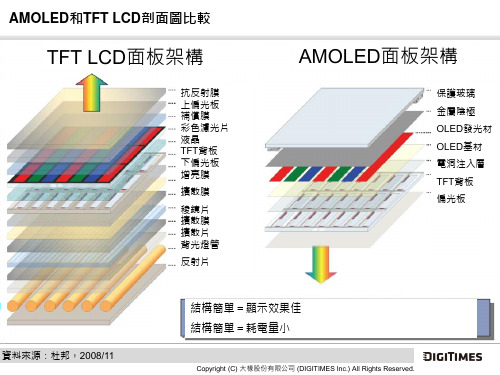
TFT LCD面板架構
抗反射膜 上偏光板 補償膜 彩色濾光片 液晶 TFT背板 下偏光板 增亮膜 擴散膜
AMOLED面板架構
保護玻璃
金屬陰極 OLED發光材 OLED基材 電洞注入層 TFT背板 偏光板
稜鏡片 擴散膜 擴散片 背光燈管
反射片
結構簡單=顯示效果佳 結構簡單=耗電量小
Japan Display
LTPS
3
4.5 5.5
550mm×670mm
730mm×920mm 1,300mm1,500mm 730mm×920mm 320mm×400mm 550mm×650mm
TMD
石川縣能美郡 石川縣能美市
4.18萬平方米 未定 2.15萬平方米 0.27萬平方米 0.89萬平方米
日立 Ortus 京瓷
千葉縣茂原市 高知縣南國市 滋賀縣野洲市
LTPS HAST LTPS
4.5 1 3
合計總月產能面積:10.43萬平方米(不計產能未定的5.5代線)
資料來源:各廠商,DIGITIMES整理,2011/9
Copyright (C) 大椽股份有限公司 (DIGITIMES Inc.) All Rights Reserved.
4.5 LTPS 5.5
基板尺寸
730mm×920mm
滿載月產能
4.8萬片 2.4萬片;至 2012年第3季 將達10萬片
面積
3.22萬平方米 4.68萬平方米;至 2012年第3季將達 19.5萬平方米
1,300mm×1,500mm
資料來源:Samsung Mobile Display,DIGITIMES整理,2011/9
1,300mm×1,500mm 730mm×920mm 1,300mm×1,500mm
oled标准teg
OLED标准TEG一般指OLED超薄透明显示屏,是一种具有超薄、超透明、低功耗、高亮度、快速响应、可柔性等特点的显示屏产品。
OLED超薄透明显示屏具有以下优点:
体积小巧:因为超薄透明显示屏的薄度可以达到0.88mm,所以体积小巧。
耐用性强:超薄透明显示屏的耐用性很强。
超薄:厚度仅为0.7mm,达到超薄化设计。
超透明:透光率高达85%,提升显示效果。
低功耗:比普通LCD显示屏节省能耗50%以上。
高亮度:亮度可达到600nit,满足不同场景的使用需求。
快速响应:反应速度快,无论是游戏还是视频,都能流畅呈现。
可柔性:可弯曲,满足不同设计的需求。
总的来说,OLED超薄透明显示屏的标准TEG具有很多优点,可以满足不同领域的需求。
oled 4t1c补偿电路

oled 4t1c补偿电路
OLED(Organic Light-Emitting Diode)是一种有机发光二极管技术,能够在电流通过时发光。
4T1C补偿电路是指四晶体晶体管电容(4T1C)的补偿电路,用于OLED显示器中的像素驱动电路。
这种补偿电路的作用是减少OLED显示器在长时间使用后出现的老化效应,以提高显示器的寿命和性能稳定性。
4T1C补偿电路的原理是通过对OLED像素的电容值进行动态调整,以抵消OLED材料老化和使用过程中产生的电容漂移现象。
这种电路通常由传感器、控制逻辑和电容调节单元组成。
传感器用于检测OLED像素的电容变化,控制逻辑根据传感器的反馈信号计算出需要调整的补偿值,然后电容调节单元对OLED像素的电容进行调整。
4T1C补偿电路的设计考虑到OLED显示器长时间使用后,像素的电容值会发生变化,导致亮度和色彩的不均匀性。
通过实时监测和调整电容值,可以有效地延长OLED显示器的使用寿命,并提高显示质量和稳定性。
总的来说,4T1C补偿电路在OLED显示器中起着至关重要的作
用,它能够有效地解决OLED像素老化和电容漂移等问题,提高显示
器的性能和可靠性。
希望这个回答能够帮助你更好地理解这个话题。
LCD驱动集成电路TM1729规格书V1.0
--
最小值 -
2.5 0.6 1.3 100 100 1.3 0.6 0.6 0.6
TM1729 典型值
-
最大值 0.3 0.3 -
单位
us us us us us ns ns us us us us
8.4. 二线串行数据传输时间波形
SDA
t BUF
t LW
SCL
SDA
t HD:STA
tr
t SDH
SDA SCL
开始条件
停止条件
在利用2线I/F输入命令以及数据时必须形成开始条件和停止条件的固有形态发生。
Slave_Address S0 1111100AC
COMMAND
A C DISPLAY DATA A P
开始条件
ACK 命令或数据判定位
停止条件
本芯片在输入命令或显示数据时,必须按照以下步骤:
©Titan Micro Electronics
V1.0
2
6. 输入/输出等效电路
VDD
VDD
VLCD
GND
GND
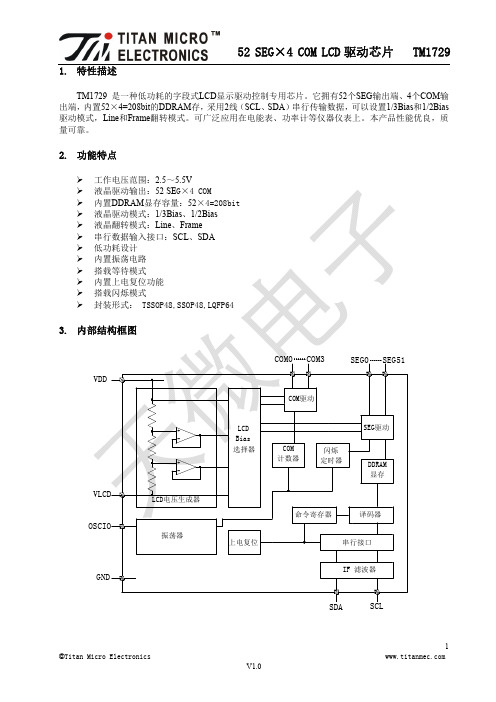
52 SEG×4 COM LCD 驱动芯片 TM1729
VDD TEST1
GND
VDD TEST2
GND
SDA
SCL
VDD
OSCIO
GND
GND
GND
2. 功能特点
工作电压范围:2.5~5.5V 液晶驱动输出:52 SEG×4 COM 内置DDRAM显存容量:52×4=208bit 液晶驱动模式:1/3Bias、1/2Bias 液晶翻转模式:Line、Frame 串行数据输入接口:SCL、SDA 低功耗设计 内置振荡电路 搭载等待模式 内置上电复位功能 搭载闪烁模式 封装形式: TSSOP48,SSOP48,LQFP64
新材料板块周观点:LGD推出77寸OLED面板,OLEDTV加速推广

万联证券证券研究报告|化工LGD 推出77寸OLED 面板,OLED TV 加速推广强于大市(维持)——新材料板块周观点日期:2021年01月18日市场回顾:⚫ 上周新材料板块上涨1.59%,同期沪深300下跌0.68%,新材料板块领先大盘2.27个百分点。
从个股来看,上周新材料板块表现良好,板块中92只个股有51只上涨,跑赢大盘的有56只股票。
涨幅前五的分别是彩虹股份(32.17%)、鼎龙股份(18.82%)、安集科技(16.01%)、金丹科技(15.57%)、沃特股份(15.21%);跌幅前五的分别是奥克股份(-17.03%)、光威复材(-12.76%)、东方钽业(-10.83%)、凯美特气(-9.50%)、道明光学(-9.21%)。
投资要点:⚫ LCD :1月12日,全球化学和特种材料公司塞拉尼斯宣布计划在我国投资建设世界级多相液晶聚合物(LCP )聚合工厂以满足其高性能LCP 产品线显著的增长需求。
本次投资总规模为年产2万吨LCP ,预计项目第一阶段将于2024年投产。
项目建设完成后塞拉尼斯将成为在北美、欧洲和中国拥有LCP 符合生产线的企业。
现阶段,全球有超过50%的LCP 均产自我国。
塞拉尼斯选择在技术较为成熟的我国建设LCP 产线,满足了其下游客户对LCP 产品快速增长的需求,同时也印证了我国LCP 生产实力在国际上的认可程度。
⚫ OLED :近日,LGD 在CES 2021上公开了一款新一代77寸OLEDTV 面板,将有机发光元件的基础有机物材料改进为高效材料并增加了1层实际发光的发光层,使面板光效率提升了约20%。
发光效率和亮度的提升使得面板呈现出的画质更加清晰,用户观看体验更加优质。
自2013年推出第一款OLED TV 面板至今,LDG OLED TV 面板的性能、产线均在不断突破和创新,OLED TV 出货量也在快速提升。
随着OLED 面板在电视等大尺寸显示领域渗透率的加速提升,对上游OLED 材料的需求也将快速上涨,利好相关龙头企业。
朗讯OLS 1.6T DWDM系统OTU告警详解

朗讯OLS 1.6T DWDM系统OTU告警详解
陈学民
【期刊名称】《山东通信技术》
【年(卷),期】2006(26)4
【摘要】朗讯公司OLS 1.6T DWDM系统可在C波段和L波段上最多支持160路10Gbit/s信号,在国内电信运营商中广泛应用.其中在中国电信南沿海干线上应用的C波段80×10Gbit/s系统,目前已接近满配置,部分段落已经满配置,是我国迄今为止实际建成的最高速率的传输系统之一.OLS 1.6T的告警情况与其他设备有很大不同,尤其是与OTU有关的告警,因此熟练掌握OTU相关告警,对做好该系统的维护工作至关重要.
【总页数】3页(P41-43)
【作者】陈学民
【作者单位】福州电信分公司,福州,350000
【正文语种】中文
【中图分类】TN91
【相关文献】
1.DWDM系统中光信号监控单板介绍及常见告警分析 [J], 张晓;任勤雷;雷庆锋
2.阿尔卡特朗讯Wave Star OLS 1.6TDWDM系统OTU告警案例详解 [J], 陈学民
3.DWDM系统中OTU中继功能的应用 [J], 周蓉
4.朗讯OLS 1.6T DWDM系统OTU告警详解 [J], 陈学民
5.朗讯OLS 1.6T DWDM系统OTU告警详解 [J], 陈学民
因版权原因,仅展示原文概要,查看原文内容请购买。
液晶显示器测量标准VESA FPDM2 update2005
1
FPDM UPDATE 050519 — page 1
1
ficiency that he has detected. However, this does not preclude the use of the FPDM to determine if a display satisfies its claimed specifications if those specifications are based upon FPDM measurements, no matter who is involved. int(x) – Integer part of x. If x = 3.8, then int(x) = 3. frame, frame rate – The frame rate is the frequency in Hz at which video information can be changed. If the display employs interlacing then this rate is called the field rate and several (normally two) fields are spoken of as composing one frame. Thus for some interlace technologies where two fields at 60 Hz create one frame, the field rate is 60 Hz where the frame rate is 30 Hz. This frame rate is not any sub-frame rate that may be at a higher frequency in order to make the display perform correctly or better. Frame rate or field rate refers to the rate at which information can be presented to the viewer. It is often between 59 Hz and 96 Hz. Some displays that have a frame rate of 60 Hz may run the display at 120 Hz in order to reverse the polarity on the pixel, but the information can only be changed at the 60 Hz frame rate. Some color sequential displays operate at 180 Hz, but the information is changed at the frame-rate of 60 Hz. native pixel array, native pixel format, native resolution (avoid) – The largest pixel array available to present information on a display. The term generally refers to using all the pixels to present information without scaling the image. It is the highest resolution that the display can offer where each pixel can display the full range of colors. “Resolution” refers to the finest detail that the optical device (or eye) can see and should not be used in referring to pixel arrays. However, the term “resolution” used to describe the format is so ingrained in the display industry that we include it here for reference only. We would prefer that “pixel array” or “pixel format” be used instead. (See “pixel array” in FPDM2.) It is an optimal or preferred format for a non-pixelated display (e.g. CRTs). pixel array – The array of pixels, usually rectangular, used to present information. Often people call this the display resolution. refresh, refresh rate, refresh period – The refresh rate is the same as frame (or field) rate. It is the frequency at which information can be changed. Many technologies refresh the information on the screen at the frame rate. The refresh period is the inverse of the frame (or field) rate.
OLED介绍
绿光膜
蓝光膜
蓝光膜
红光膜
红光膜
O
蒸镀、抬离红膜
蒸镀、抬离红膜
FAHED——简介
发光原理:
在薄膜结构的上下电极之间施加反向电压
电子从上电极通过传输层达到传输层和绝缘层之间的界面
当施加正向电压时
电子就会获得加速穿过传输层达到上电极, 能量大的电子能克服势垒穿过上电极逸出到真空中形成发射电子
OLED——象素结构图
OLED——产品结构图
OLED——工艺流程
OLED——空穴注入(HIL)材料
OLED——空穴传输(HTL)材料
空穴传输材料
Tg(℃)
TPD
60
NPB
78
TTB
82
HTM2
98
OLED——掺杂材料
OLED——电子传输、发光层材料
OLED——电子传输材料
OLED——驱动方式
OLED 自发光 >160度宽视角 相应快,1us 更薄,<1mm 柔性显示 工艺简单,具有低成 本潜力 使用温度范围宽 : -40℃ ~ 85 ℃
OLED——Vs LCD(色彩亮度对比)
OLED——Vs LCD(视角对比)
OLED——Vs LCD(性能)
OLED——Vs LCD(剖面结构)
OLED——简介
OLED又称有机发光二极管 可以自发光,无需背光 全固态,不怕震动 高亮度 高对比度 视角宽 超薄 低成本 低功耗 பைடு நூலகம்
OLED——在显示器中的分类
OLED
OLED——应用
小尺寸OLED (1~7英寸)
介电薄膜
金属行电极
玻璃基板
色彩转换膜
ITO列电极
TDA8933BTW中文资料
2. Features
Operating voltage from 10 V to 36 V asymmetrical or ±5 V to ±18 V symmetrical Mono bridge-tied load (full-bridge) or stereo single-ended (half-bridge) application Application without heat sink using thermally enhanced small outline package High efficiency and low-power dissipation Thermal foldback to avoid audio holes Current limiting to avoid audio holes Full short circuit proof across load and to supply lines (using advanced current protection) I Internal or external oscillator (master-slave setting) that can be switched I No pop noise I Full differential inputs I I I I I I I
[1] [2]
7.5 9.3
8.5 10.3
-
W W
15.4 18.9
17.1 20.6
-
W W
Rs is the total series resistance of an inductor and an ESR single-ended capacitor in the application. Output power is measured indirectly, based on RDSon measurement.
基于L1L2极限学习机的熔池熔透状态识别
基于L1L2极限学习机的熔池熔透状态识别0 序言焊接过程中熔池形态变化受高热能、焊接材料、保护气体等多方面因素影响的复杂、非线性的物理过程. 熔池形态与焊接质量好坏、焊缝外观形状及缺陷等密切相关.如何利用视觉传感技术正面观察熔池形态,了解焊接过程中熔化金属的动态变化行为,是当前智能焊接领域中的研究热点之一[1-3].神经网络凭借其较好的鲁棒性和容错能力成为熔池形态分析方法中的一个热点研究方向. 文献[4]利用BP神经网络建立熔池面积、熔宽等几何特征与熔透状态之间的关系模型,并获得了较好的熔透状态识别效果. 文献[5]结合遗传算法和BP神经网络建立熔池形态与焊缝形状之间的关系模型,利用焊接过程中的熔池形态成功预测焊缝的高度和宽度. 文献[6]利用Kohonen神经网络来识别GMAW焊接过程中干扰种类. 传统神经网络在分析焊接图像时也有一些不足,如对训练数据量需求较大、网络收敛速度慢、容易过学习等,使其无法满足智能焊接实时性、准确性的要求,限制了其在工业中的进一步应用.极限学习机(ELM)是近年来兴起的一种生物学习网络[7-8],在利用ELM进行熔池形态分析时,不需要建立对象的精确数学模型,也不需要深入了解对象的特性,仅通过对有限样本进行训练和学习就可以完成对特定对象的识别,具有计算简单、学习速度快的特点.传统ELM框架随机设定输入和隐层参数,仅采用伪逆算法估计输出权重,存在容易过学习、算法泛化能力低的问题. 文中结合熔池图像特征,提出一种基于L1/L2范数正则化约束的极限学习机算法(L1/L2-ELM)来对熔池的形态(全熔透、未熔透、过熔透)进行识别. 首先利用主成分分析(PCA)对原始数据进行降维,把降维后的数据送入网络;其次在传统ELM基础上,在估计输出权重时引入L1范数约束来控制整个模型的复杂度,提高模型泛化能力. 另外试验中发现熔池图像中单一的像素点并没有实际研究意义,有意义的熔池图像特征都以“团块”形式出现,通过引入L2范数约束来对ELM的输出权重进行平滑,以获取熔池图像中的“团块”特征. 试验结果表明,文中所提出的L1/L2-ELM算法训练时间短、泛化能力强,对全熔透、未熔透、过熔透三种状态的识别准确率取得了较好的效果.1 熔池图像处理1.1 图像采集所采用的试验装置如图1所示,主要包括控制系统、图像处理系统、视觉传感系统、焊枪、行走机构、焊接工作台. 图像的采集工作通过视觉传感系统完成. 熔透点通过人工加大电流方式来设置(熔透电流阈值由焊接板材和板厚决定[9]),焊接完成后再将熔池图像与熔透过程对应起来.图1 试验装置示意图Fig.1 Diagram of experimental device试验系统中焊机为山大奥太NBC-350逆变式CO2气体保护焊机,焊丝直径为1.2 mm,焊丝伸出长度为10 mm,焊丝材料为ER50-6,焊件采用厚度1.5 mm的镀锌板,焊缝间隙小于0.1 mm.焊接方式为平板堆焊,通过大量试焊,确定焊接电流为100~140 A.试验条件如表1所示.表1 固定速度焊接试验条件Table 1 Condition of welding experiments with fixed speed焊接速度v/(mm·s–1)CO2保护气流量q/(L·min–1)图像采集速率f/s 焊接方式将熔透模式定义为三种状态:全熔透、未熔透、过熔透. 如图2所示,全熔透是指在焊接过程中,焊接母材已经完全熔化,焊缝下方小范围被熔化,焊接母材的底部已经被熔透;未熔透是指在焊接过程中,焊接母材的熔化范围没有到达焊缝底部,焊缝底部没有被熔透;过熔透是指焊接母材的熔化范围超过了焊接底部,焊缝底部绝大部分被熔化,甚至出现熔化范围超过了焊缝实际宽度的结果.图2 三种熔透状态Fig.2 Three different penetration modes为了实际对比上述三种状态的不同,如图3所示,在不同焊接条件下选取了三组熔透状态区别较为明显的焊件,通过对比焊缝正(背)部不同的熔透状态说明三种不同的熔透定义.图3 不同熔透状态所对应的实物焊缝正 (背)面形貌Fig.3 Front and back view of welding seam under different penetration modes1.2 基于 PCA 的熔池图像特征提取熔池图像的原始数据集可以表示为,其中N表示熔池图像样本数,L表示熔池图像的大小.在信息化日渐加深的今天,课题上直接传授知识的“满堂灌”已经不能起到很好的效果,学员们思维活跃,并且注意力更难以长时间的集中,需要使用学员关心的案例来激发他们的学习兴趣,提高学员课堂参与度,来达到更好的教学效果。
- 1、下载文档前请自行甄别文档内容的完整性,平台不提供额外的编辑、内容补充、找答案等附加服务。
- 2、"仅部分预览"的文档,不可在线预览部分如存在完整性等问题,可反馈申请退款(可完整预览的文档不适用该条件!)。
- 3、如文档侵犯您的权益,请联系客服反馈,我们会尽快为您处理(人工客服工作时间:9:00-18:30)。
J in-Peng Y ang ,Y an X iao ,Y an-Hong D eng ,S teffen D uhm ,N obuo U eno ,S huit-Tong L ee ,Y an-Qing L i ,*a nd J ian-Xin T ang *linked in series by interconnectors, and the device characters such as brightness and current effi ciency at a certain current density can scale linearly with the number of EL units. [ 1 , 2 ] Upon the application of anelectric fi eld, electrons and holes gener-ated by the interconnectors will inject into the neighboring electron- and hole-trans-porting layers (ETL and HTL) of the indi-vidual EL units, and thereby recombine with holes injected from the anode side orelectrons injected from the cathode side for light emission. [ 10–15 ] Therefore, the interconnectors that serve as the chargegeneration layer, are the critical factor for tandem OLEDs to function effi ciently. [ 1–15 ] However, the mechanism of charge gen-eration and separation within the inter-connectors is not yet understood in asuffi cient way. [ 10–19 ]T he interconnectors used in tandem OLEDs are typically a bilayer structurewith various materials, including a metal–metal (or metal oxide) bilayer, [ 9 ] an organic–metal (or metal oxide) bilayer, [ 1 , 3–7 ]or an organic–organic bilayer. [ 2, 10–12 ] In the interconnectorswith an organic–metal oxide bilayer, transition metal oxides(TM Os) such as vanadium oxide (V 2O 5), [ 4 , 15 ]molybdenum tri-oxide (M oO 3), [ 5 , 16 ] and tungsten trioxide (WO 3), [ 7 , 9 ]are widely incorporated adjacent to the HTL of the neighboring EL unitdue to their high work function and highly optical transparencyin the visible region for photon output, while the organic layers adjacent to the ETL of another neighboring EL unit are com-monly n-typed doped by alkaline metals or metal compounds (e.g., Li, Cs, Cs 2C O 3,etc). [ 2 , 5 , 13 ] P arallel to various structures employed as the interconnectors in tandem OLEDs, several models have been proposed to inter-pret the charge carrier generation and separation process. [ 10–19 ] Kröger et al. proposed a temperature-independent tunneling-based charge generation model in doped organic–organic bilayer interconnectors via electric-fi eld-induced electron transfer from the highest occupied molecular orbital (HOM O) of a p-type doped organic layer to the lowest unoccupied molecular orbital(LUM O) of an n-type doped organic layer, [ 14 ] which was sup-ported by the energy level alignment obtained from the ultra-violet photoemission spectroscopy (UPS) measurements. [ 10 , 11 ] On the other hand, the mechanisms operating at TMO-organicElectric-Field-Assisted Charge Generation and Separation Process in Transition Metal Oxide-Based Interconnectors for Tandem Organic Light-Emitting DiodesT he charge generation and separation process in transition metal oxide (TMO)-based interconnectors for tandem organic light-emitting diodes(OLEDs) is explored using data on electrical and spectral emission proper-ties, interface energetics, and capacitance characteristics. The TMO-based interconnector is composed of MoO 3 and cesium azide (CsN 3)-doped 4,7-diphenyl-1,10-phenanthroline (BPhen) layers, where CsN 3 is employedto replace the reactive metals as an n-dopant due to its air stability and lowdeposition temperature. Experimental evidences identify that spontaneouselectron transfer occurs in a vacuum-deposited MoO 3 layer from various defect states to the conduction band via thermal diffusion. The external electric-fi eld induces the charge separation through tunneling of generated electrons and holes from MoO 3 into the neighboring CsN 3-doped BPhen and hole-transporting layers, respectively. Moreover, the impacts of constituentmaterials on the functional effectiveness of TMO-based interconnectors andtheir infl uences on carrier recombination processes for light emission have also been addressed. D OI: 10.1002/adfm.201102136 J.-P. Y ang ,Y . X iao ,Y .-H . D eng ,P rof. Y .-Q. L i ,P rof. J.-X. T ang Jiangsu Key Laboratory for Carbon-Based Functional Materials & DevicesInstitute of Functional Nano & Soft Materials (FUNSOM)Soochow University Suzhou 215123, P. R. China E -mail: y qli@; jxtang@ D r. S. D uhm ,P rof. N. U eno Graduate School of Advanced Integration ScienceChiba University1-33 Yayoi-cho, Inage-ku, Chiba 263-8522, Japan P rof. S.-T. L ee Center Of Super-Diamond and Advanced Films (COSDAF)City University of Hong KongHong Kong SAR, P. R. China 1. IntroductionI n recent years, tandem organic lighting emitting diodes (OLEDs) have been attracting more attention for the develop-ment of next-generation fl at panel displays and solid-state lighting, because of their advantages with high brightness, long lifetime, and low energy consumption. [ 1–12 ] In tandem OLEDs, vertically stacked electroluminescent (EL) units are electrically2. R esults and Discussion2.1. Infl uence of Interconnectors on DeviceCharacteristicsTandem OLEDs were fabricated with two individual EL units, which were separated by different interconnectors, namely (1)CsN 3:BPhen/M oO 3 , (2) CsN 3:BPhen, (3)MoO 3, and (4) none. The EL unit is com-posed of a hole-transporting layer (HTL) of N ,N ′-di(naphthalene-1-yl)-N ,N ′-diphenyl-benzidine (NPB), a green emitting layer of tris(8-hydroxyquinoline) aluminum (Alq 3)doped with 10-(2-benzothiazolyl)-2,3,6,7-tet-rahydro-1,1,7,7-tetramethyl-1H,5H,11H-(1)benzopyropyrano(6,7,8-i,j)quinolizin-11-one(C545T), and an electron-transporting layer (ETL) of BPhen. The anode and cathode of the OLEDs are indium tin oxide (ITO) andLiF/Al bilayer, respectively. To minimize theeffects due to different processing condi-tions, tandem devices with four differentinterconnectors were fabricated in the samelot by changing the shadow mask. For comparison, a reference device with a single EL unit was also prepared. The detailedlayer structures of the devices are shown inT able 1 . F igure 1 plots the current-density–voltage ( J –V )characteris-tics and luminance efficiency of four tandem OLEDs (devices B–E) together with that of a reference OLED having only one EL unit (device A) for comparison. As observed in Figure 1 a , the driving voltage of the tandem OLED with a CsN 3:Bphen/MoO 3 interconnector (device B) is almost twice comparedto that of the reference device (device A) at a certain current density, which can be expected for a properly working tandemOLED. However, it is evident that the other tandem devices (devices C–E) exhibit a poor electrical property, and require ahigher driving voltage compared to the device with the use ofCsN 3:Bphen/MoO 3. T he luminance effi ciency versus current density of devices C–E is comparable with that of the reference device A with a single EL unit (Figure 1 b ). The luminance effi ciency of the tandem device B with the CsN 3:BPhen/MoO 3 interconnector is, however, almost twice than that of device A. For instance, at the current density of 20 mA cm− 2 , the luminance effi ciencies of tandem devices B–E and the reference single EL device A are 19.3, 13.7, 11.1, 6.8, and 10.1 cd A− 1 , respectively. It is clearly noted that constituent materials of interconnectors are critical in their functional effectiveness and thus the carrier recombi-nation processes for light emission in tandem OLEDs.T o gain a deeper understanding of the correlation between the carrier recombination processes and the difference in effi -ciency for tandem OLEDs with various interconnectors, twoseries of tandem devices combining green and red emission EL units (EL-G and EL-R) were further fabricated. For each series, four devices with different interconnectors were fabricated in the same lot by changing the shadow mask. The layer struc-tures of these two series (i.e., devices F–I and J–M) are shown bilayer interconnectors remain a subject of debate. [ 15–19 ]Ther-mally assisted charge generation models have been proposed, in which TMOs were assumed to be p-type semiconductors and impurity levels above the valence band of TMOs were regardedas the sources of charge generation. [ 15 , 17 ] In contrast to the claim that electrons and holes were generated at TM O/ETL inter-faces, [ 15 , 17 ] it has been supposed that charge generation and sep-aration occur at the interface between TMOs and the adjacent HTL via electron transfer from the HTL ’s HOMO into the con-duction band of TMOs. [ 12 , 16 , 18 , 19 ] Such understanding on TMO-organic bilayer interconnectors was primarily inferred from the electronic structures determined by UPS analysis, in which TM Os actually exhibit n-type semiconducting property with high work function and a deep-lying conduction band. [ 16 , 18–21 ] However, aside from various conjectures, direct evidence is yet lacking for clarifying which interface dominates the chargegeneration and separation process in TMO-based interconnec-tors, or whether the charge generation even occurs within the TMO layer.T o further understand the TM O-based interconnectors, we present a detailed study on charge generation and separation process in TM O-based interconnectors by systematically char-acterizing electrical and spectral emission properties, interface energetics, and capacitance–voltage characteristics through device fabrication, photoelectron spectroscopy, and impedance spectroscopy. The TMO-based interconnector is composed of a bilayer of M oO 3 and cesium azide (CsN 3)-doped 4,7-diphenyl-1,10-phenanthroline (BPhen). CsN 3 is employed to replace thetypical reactive metals as an n-type dopant in the interconnector, because of its air stability and low deposition temperature dem-onstrated recently in tandem OLEDs. [ 22 ] The role of TMO and n-type doped organic layers in charge generation and separa-tion, and their infl uence on the carrier recombination processes for light emission in tandem OLEDs have been identifi ed.T able 1. L ayer structures of the OLED devices.Devices or units Layer structuresDevice A ITO/E L /LiF (0.5 nm)/Al (100 nm)Device B ITO/ E L /CsN 3 :BPhen (20 vol%, 20 nm)/MoO 3 (10 nm)/ E L /LiF (0.5 nm)/Al (100 nm)Device CITO/ E L /MoO 3 (10 nm)/E L /LiF (0.5 nm)/Al (100 nm)Device D ITO/ E L /CsN 3:BPhen (20 vol%, 20 nm)/ E L /LiF (0.5 nm)/Al (100 nm)Device E ITO/ E L /E L /LiF (0.5 nm)/Al (100 nm)E L NPB (40 nm)/C545T:Alq 3 (1 vol%, 20 nm)/BPhen (40 nm)DeviceF ITO/ E L-R /CsN 3 :BPhen (20 vol%, 20 nm)/MoO 3 (10 nm)/E L-G /LiF (0.5 nm)/Al (100 nm)DeviceG ITO/ E L-R /MoO 3 (10 nm)/E L-G /LiF (0.5 nm)/Al (100 nm)Device H ITO/ E L-R /CsN 3 :BPhen (20 vol%, 20 nm)/ E L-G /LiF (0.5 nm)/Al (100 nm)Device I ITO/ E L-R /E L-G /LiF (0.5 nm)/Al (100 nm)Device J ITO/ E L-G /CsN 3 :BPhen (20 vol%, 20 nm)/MoO 3 (10 nm)/ E L-R /LiF (0.5 nm)/Al (100 nm)Device K ITO/ E L-G /MoO 3 (10 nm)/ E L-R /LiF (0.5 nm)/Al (100 nm)Device L ITO/ E L-G /CsN 3:BPhen (20 vol%, 20 nm)/ E L-R /LiF (0.5 nm)/Al (100 nm)Device M ITO/ E L-G /E L-R /LiF (0.5 nm)/Al (100 nm)E L-G NPB (40 nm)/Alq 3 (20 nm)/BPhen (40 nm)E L-R NPB (40 nm)/DCJTB:Alq 3 (3 vol%, 20 nm)/BPhen (40 nm)in Table 1 . The EL-G comprises a NPB layer as the HTL, aBPhen layer as the ETL, and an Alq 3 layer as the green emis-sion layer, while the EL-R is formed by a red emission layer of 4-(dicyanomethylene)-2- t -butyl-6-(1,1,7,7,-tetramethyl julolidyl-9-enyl)-4H-pyran (DCJTB)-doped Alq 3 located between the HTL of NPB and the ETL of BPhen. As depicted in the insets of F igure 2 a and b, EL-G and EL-R in these two series are electri-cally connected by an interconnector in opposite sequence. F igure 2 compares the EL spectra of two series of tandemdevices at J = 5 mA cm − 2 , in which the EL peaks with a wave-length of 520 nm corresponds to Alq 3 emission, while the ELpeak at ∼ 600 nm corresponds to DCJTB emission. As shown in Figure 2 , EL spectra of tandem devices with various interconnec-tors help to identify the location of the emissive zones for these devices. With the use of the CsN 3:BPhen/MoO 3interconnector in tandem OLEDs (devices F and J), both green and red emis-sion components can be observed in Figures 2 a and b, implying that such an interconnector functions well and emissions in both EL-G and EL-R units are mutually independent on the tandem structure. Similarly, both green and red emission fea-tures can be observed in EL spectra for tandem devices with only MoO 3 as the interconnector (devices G and K), except that the emission intensity from the EL unit at the anode side is rel-atively lower than that of devices F and J with a CsN 3:BPhen/MoO 3 interconnector. The emission behaviors of devices G and K indicate that the charge generation and hole injection into the HTL of the cathode side-EL unit are consistent with the tandem devices with a CsN 3:BPhen/MoO 3interconnector, whereas the electron-hole recombination in the anode side-EL unit is prohibited due to the reduced electron injection into the neighboring ETL of BPhen without a CsN 3 :BPhen layer. On the contrary, when only CsN 3:BPhen is used in the interconnector, the tandem devices (i.e., devices H and L) behave like an OLED with a single EL unit, where the emission from the EL unit at the anode side dominates the EL spectra with negligible emis-sion from the cathode side-EL unit. For example, device H hasF igure 1. a ) J –V and b) luminance effi ciency-current density characteris-tics obtained from the single EL unit device A and tandem devices B–E with different interconnectors. The device confi gurations are shown in Table 1.F igure 2. E L spectra of tandem devices with two different EL units. a) Devices F–I: the bottom EL unit having red emission and the top EL unit having green emission; b) devices J–M: the bottom EL unit having green emission and the top EL unit having red emission, respectively.reaction takes place at CsN 3:BPhen/M oO 3 interface, and some CsN 3-doped BPhen molecules are recovered to that of pristine the emission of DCJTB from the EL-R unit and very little emis-sion of Alq 3 from the EL-G unit, while device L exhibits the reverse behavior. Similar emission behaviors can be observed for tandem devices I and M without an interconnector between two EL units, while the emission intensities are rather lower than those of devices H and L, as shown in Figure 2 a and b. The asymmetric contribution of two EL units to the EL spectra for devices H, I, L and M validates that the MoO 3 layer is essen-tial to charge generation in the interconnector.2.2. Interfacial Energetics on Interconnectors To understand the origin of the difference in device perform-ance and especially the impacts of constituent materials on the functional effectiveness of TM O-based interconnectors, the electronic structures of the interconnectors with the neigh-boring ETL and HTL layers were studied via ultraviolet and X-ray photoemission spectroscopy (UPS and XPS) measure-ments. F igure 3 a shows the HeI UPS spectra of incremental CsN 3:BPhen deposition on a 100 Å-thick BPhen layer on the underlying ITO substrate. It is obvious that deposition of the CsN 3:BPhen overlayer on BPhen leads to an abrupt and rigid shift of energy levels towards higher binding energies (BEs). The shift of the secondary electron cutoff in the high BE region indicates a vacuum level (VL) shift of 1.1 eV, as shown in Figure 3 a . The HOM O edges of CsN 3:BPhen and pristine BPhen can be extracted by the intercept of the tangent of the leading edges of the low BE feature and the background level, and are found at 4.4 and 3.3 eV below Fermi level ( E F ), respec-tively. The ionization potential (IP) values, which were obtained by the energy difference between the HOM O edge and VL onset, are 6.4 eV for both CsN 3:BPhen and BPhen, respectively, and are thus in good agreement with previous data. [ 19 ]I n addition, two gap states with energy difference of 2.7 eV were formed in the energy gap of CsN 3:BPhen as shown in the inset of Figure 3 a . [ 19 ] To accurately determine the chemical reac-tions at the BPhen/CsN 3:BPhen interface, XPS measurements were also taken after each deposition step. F igure 4displays the evolution of XPS spectra of C 1s, N 1s and Cs 3d5 core levels for the BPhen/CsN 3:BPhen interface. As evident in Figures 4 a and b, C 1s and N 1s core levels exhibit an abrupt shift of ∼1.2 eV towards higher BE with the appearance of a new feature at the low BE region upon the deposition of CsN 3:BPhen, which are consistent with the UPS results. As reported in the literature, CsN 3 was expected to have an n-doping effect through thedecomposition into Cs and N 2 during the evaporation. [ 22 ]There-fore, the new peaks in C1s and N1s core level spectra repre-sent chemical bonding among Cs, C and N in the CsN 3:BPhenlayer.T he HeI UPS spectra of MoO 3 deposited onto CsN 3:BPhen layer are shown in Figure 3 b , in which the bottom spectrum is identical to that of 100 Å-thick CsN 3:BPhen layer in Figure 3 a . It is evident that deposition of the M oO 3 overlayer results in a progressive shift of emission features of CsN 3:BPhen and M oO 3 toward lower BEs, and the disappearance of the CsN 3 :BPhen gap states, however, a M oO 3-derived gap state is emerging (vide infra). Similar to a previous report, [ 19 ] the M o3d core level spectra (not shown here) imply that a chemicalF igure 3.H eI UPS spectra of BPhen/CsN 3 :BPhen (a) and CsN 3:BPhen/MoO 3 (b) interfaces as a function of incremental deposited layers. The inset shows the enlarged HOMO region of 100 Å-thick CsN 3:BPhen layer.BPhen via the reduction of Mo 6 + cations to Mo 5 + state. In con-trast, the UPS spectral evolution of the BPhen/MoO 3interface (not shown here) indicates the chemically inert nature without additional spectral structures upon MoO 3 deposition on BPhen layer. However, it is noted that the spectral features become sat-urated at 50 Å-thick MoO 3 layer, and are identical to that at the CsN 3:BPhen/M oO 3interface. [ 19 ] A ccording to the top spectrum in Figure 3 b , a 100 Å-thick MoO 3 layer possesses a high work function of 6.7 eV with the valence band maximum at 2.8 eV below E F, which is consistent with previous reports. [ 19 , 20 ] Given that the energy gap of MoO 3isaround 3.1 eV, [ 20 ] the MoO 3 layer thus exhibits n-type semicon-ducting property with the conduction band minimum pinnedslightly above E F . In addition, it is obvious that deep-lying gap state emerges in the forbidden gap of M oO 3, which is related to the oxygen defi ciency and partial reduction of M o 6 + cation in accordance with XPS measurement in the literature. [ 19 , 20 , 23 , 24 ]The density of these gap states is so high that they not only dic-tate the position of the Fermi-level but may also act as a charge reservoir.F igure 5 displays the UPS spectra of a 100 Å-thick NPB layer incrementally deposited on M oO 3 , BPhen, and CsN 3:BPhen substrates, respectively. No evidence of chemical reaction or formation of new interfacial electronic states can be observed for these three interfaces, which are in good agreement withprevious data. [ 19 , 20 , 23 , 24 ] At the same time, these interfacesexhibit two different trends upon interface formation. The VL shift to higher BE side represents the formation of an interface dipole upon deposition of NPB on M oO 3 , whereas the UPS spectra evolutions of CsN 3:BPhen/NPB and BPhen/NPB inter-faces imply the absence of interface dipole at the corresponding interfaces. F igure 4. T he evolution of (a) C 1s, (b) N 1s, and (c) Cs 3d 5/2 core level XPS spectra upon the formation of the BPhen/CsN 3 :BPhen interface. The dashed lines are added just for the guide for eyes.F igure 5. H eI UPS spectra of a 100 Å-thick NPB deposited on MoO 3,BPhen, and CsN 3:BPhen substrates, respectively.MoO 3 with a small hole injection barrier height. It has alsobeen demonstrated that the hole-injection property of ambient contaminated M oO 3 surface is not significantly infl uenced, although the contamination reduces the work function of a low vacuum-grown M oO 3 film by about 1 eV with respect to the freshly evaporated fi lm. [ 25–27 ] Therefore, it is expected that anelectric-fi eld-assisted charge generation and separation process can easily occur at the M oO 3/NPB interface via hole injection from M oO 3 into NPB’s HOM O, as suggested previously.[ 13 , 23 ] However, the charge generation process could also happen within the TM O layer by exciting electrons from the oxygen vacancy derived gap states to the conduction band. The incor-poration of a doped n-type organic layer in TM O-based inter-connectors is also essential for tandem OLEDs to function effi -ciently with enhanced EL effi ciency. As shown in Figure 6 a and c, doping CsN 3 into BPhen can greatly move E F to only 0.1 eV below the LUM O, resulting in enhancing the electron injec-tion and transport through CsN 3:BPhen into the BPhen ETL. Accordingly, electrons generated in MoO 3 can easily inject into CsN 3:BPhen ’s LUM O due to the small injection barrier at theF igure 6 depicts the energy level diagrams for the dis-cussed interconnectors obtained from UPS spectra: a) BPhen/CsN 3:BPhen/M oO 3 /NPB, b) BPhen/M oO 3 /NPB, c) BPhen/CsN 3:BPhen/NPB, and d) BPhen/NPB on ITO substrate, respectively. Here, HOM O (or valence band) positions are extracted from the UPS spectra, and LUMO (conduction band) positions are estimated by adding the charge-transport gaps (4.2 eV for BPhen, 4.5 eV for CsN 3:Bphen, 4.0 eV for NPB, and 3.1eV for MoO 3) relative to the HOMO energy levels. [ 16 , 19 , 20 , 23 ] E F of the underlying ITO substrate was used as energy refer-ence, which was aligned across the interfaces in a thermody-namic equilibrium state. The contributions of interface dipole and energy level bending to the VL shift at the interfaces are taken into account in the energy level diagrams.A ccording to the energy level diagrams of the interconnec-tors with neighboring HTL and ETL layers depicted in Figure 6 , the functional effectiveness of MoO 3-based interconnectors and thus the device performance of the corresponding tandem OLEDs shown in Figures 1 and 2 can be understood. As shown in Figure 6 a and b, a p–n junction is formed between NPB and F igure 6. S chematic energy level diagrams: a) BPhen/CsN 3:BPhen/MoO 3 /NPB, b) BPhen/MoO 3 /NPB, c) BPhen/CsN 3 :BPhen/NPB, and d) BPhen/NPB interfaces on ITO substrate, respectively. All the values shown are in the unit of eV.is normalized by the zero bias capacitance ( C 0 ). It is observedthat the capacitance for devices with M oO 3 in the intercon-nector (i.e., devices N and O) shows an abrupt increase when the forward bias exceeds a certain value, while no change incapacitance is observed under reverse bias. However, the capac-itance of devices without MoO 3 (i.e., devices P and Q) is almost constant in the bias range, indicating neither displacement norgeneration of charges within NPB and CsN 3:BPhen (or BPhen) layers. Therefore, the change in capacitance under forward bias is defi nitely associated with the presence of MoO 3 layer, wheregenerated charges are transported through organic layers. Theseobservations are consistent with the results in Figure1 that no charge generation occurs in tandem OLEDs without M oO 3in the interconnectors.T o identify the role of individual Cs 2C O 3:BPhen, M oO 3and NPB layers in the change of capacitance, also C –V character-istics of devices R–U were examined at a fi xed frequency of 1 kHz (seeF igure 8 ). An increase of capacitance under forward bias can be observed in the case of device R, although the HTL CsN 3:BPhen/M oO 3 interface. However, the large LUMO offset at the M oO 3/BPhen interface (see Figure 6 b ) limits the effec-tive injection of electrons from M oO 3 into the BPhen layer of the ITO-side EL unit unless a higher driving voltage is added. Due to the insuffi cient electron injection and exciton formation, the resulting emission from the ITO-side EL unit is thus smaller than that of tandem OLED with a CsN 3:BPhen/M oO 3 interconnector. F igures 6 c and d show a typical fl at vacuum level alignment at CsN 3 :BPhen/NPB and BPhen/NPB interfaces, when M oO 3 was not involved in interconnectors. The large energy level offset between NPB’s HOM O and CsN 3:BPhen ’s (or BPhen ’s) LUM O indicates that charge generation process is hard to occur at CsN 3:BPhen/NPB and BPhen/NPB interfaces unless a higher driving voltage is applied. In addition, the CsN 3:BPhen or BPhen layer could exhibit excellent hole-blocking capability for the emission layer of Alq 3 due to the wide bandgap and the large IP value. Therefore, the electron–hole recombination in the cathode-side EL unit for tandem OLEDs using interconnec-tors without MoO 3 is eliminated due to the lack of charge gener-ation by MoO 3 and leakage current of holes from the ITO side.This is the reason why intensive emission from the cathode-side EL unit can only be observed for tandem OLEDs with MoO 3in the interconnectors, while other tandem devices behave like an OLED with a single EL unit, as shown in Figure 2 .2.3. Charge Generation Process in Interconnectors by Capacitance–Voltage MeasurementsT o further verify the electric fi eld-assisted charge generation and separation process in TM O-based interconnectors, model devices were fabricated with a double-insulating structure of ITO/LiF/BPhen/Interconnector/NPB/LiF/Al (as shown in T able 2 ) and the corresponding capacitance-voltage ( C –V )char-acteristics were measured under external electric fi elds. The forward bias in the C –V measurement was defi ned as the ITO electrode applied positively. The double-insulating layers of LiF were used to prohibit the charge injection from external electrodes, because it is usually diffi cult to be distinguished experimentally from the internal behaviors in the measured current fl ow.F igure 7 shows the capacitance of model devices with var-ious interconnectors as a function of external DC bias at a fi xed frequency of 1 kHz, where the measured capacitance (C) T able 2. L ayer structures of double-insulating model devices for capacitance measurement.Devices Layer structuresDevice N ITO/LiF (20 nm)/BPhen (40 nm)/CsN 3 :BPhen (20 vol%, 20 nm)/MoO 3 (10 nm)/NPB (40 nm)/LiF (20 nm)/Al (100 nm)Device O ITO/LiF (20 nm)/BPhen (40 nm)/MoO 3 (10 nm)/NPB (40 nm)/LiF (20 nm)/Al (100 nm)Device P ITO/LiF (20 nm)/BPhen (40 nm)/CsN 3 :BPhen (20 vol%, 20 nm)/NPB (40 nm)/LiF (20 nm)/Al (100 nm)Device Q ITO/LiF (20 nm)/BPhen (40 nm)/NPB (40 nm)/LiF (20 nm)/Al (100 nm)Device R ITO/LiF (20 nm)/BPhen (40 nm)/CsN 3 :BPhen (20 vol%, 20 nm)/MoO 3 (10 nm)/LiF (20 nm)/Al (100 nm)Device S ITO/LiF (20 nm)/BPhen (40 nm)/CsN 3 :BPhen (20 vol%, 20 nm)/MoO 3 (10 nm)/CsN 3 :BPhen (20 vol%, 20 nm)/LiF (20 nm)/Al (100 nm)Device T ITO/LiF (20 nm)/NPB (40 nm)/MoO 3 (10 nm)/NPB (40 nm)/LiF (20 nm)/Al (100 nm)Device UITO/LiF (20 nm)/BPhen (40 nm)/MoO 3 (10 nm)/BPhen (40 nm)/LiF (20 nm)/Al (100 nm)F igure 7.C –V characteristics of the interconnector device with a double-insulating structure measured at a fi xed frequency of 1 kHz. C 0 is the zero bias value of capacitance. The inset shows the device structure.derived deep-lying defect states below E F, which is observed in UPS and thus considerably high. Therefore, electron transfer in MoO 3 is expected to spontaneously occur via thermal diffusion from various defect states to the conduction band [denoted as process (1) in Figure 9 ]. Under forward bias, the electric fi eld within M oO 3 layer induces tunneling of electrons and holes into the LUM O of Cs 2C O 3:BPhen and the HOM O of NPB [processes (2) and (3)], respectively. Then, electrons will imme-diately be driven away from Cs 2C O 3 :BPhen to the BPhen layer by the external electric fi eld, while holes are in the same way moved away from the interface. Such a displacement of charges at Cs 2C O 3:BPhen/M oO 3 and MoO 3/NPB interfaces gives rise to the capacitance changes, as shown in Figures 7 and 8 . When the bias is inverted, no injection of electrons and holes occurs at Cs 2C O 3:BPhen/M oO 3 and MoO 3/NPB interfaces, exhibiting the unchanged capacitance. Although the proposed charge generation and separation process [processes (1–3) in Figure 9 ]is different from the mechanisms reported previously, [ 13 , 16 ]inwhich electrons were transferred from the NPB’s HOMO to the TMO’s conduction band, and then moved to the n-type doped organic layer [processes (4) and (2)], our experimental results do not exclude that such a process happens additionally. How-ever, it is important for further device design to take in mind that the high density of intrinsic M oO 3 gap states closes the gap of 3.1 eV to a few hundred meV and thus leads to the con-comitant n- and p-type behavior of M oO 3 . The density of the MoO 3 oxygen vacancies derived gap states can be increased byvacuum-annealing, [ 20 ] and even more importantly for actualdevices, also prevails for ex situ processed MoO 3.[ 25 ]3. Conclusions I n summary, the functionality of TM O-based interconnec-tors for tandem OLEDs is demonstrated by systematicallyof NPB was removed as compared to device N in Figure 7 . Thisresult clearly indicates that the MoO 3/NPB interface is not the unique factor contributing to the charge generation process for TM O-based interconnector, which is contrary to the proposedmechanism reported in the literature. [ 13 , 16 ] Compared to deviceR, an additional Cs 2C O 3 :BPhen layer was inserted between MoO 3 and LiF layers in device S, leading to capacitance changes under both forward and reverse biases. Similar behaviors were observed for device T with a M oO 3 layer between two NPB layers. On the contrary, no change in capacitance in the applied bias range was evident for device U, where the MoO 3 layer was sandwiched between two BPhen layers. This is due to the large energy offset between BPhen ’s LUM O and M oO 3’s conduc-tion band as shown in Figure 6 b , which is unfavorable to the electron injection from M oO 3 into the BPhen layer and thus limits the change in capacitance. These results defi nitely indi-cate that both Cs 2C O 3:BPhen/M oO 3 and MoO 3/NPB interfaces contribute to the charge separation process, although charges were generated within the M oO 3 layer. In addition, it can be understood that the non-monotonic dependence of capacitance on bias voltage for device N in Figure 7 is due to the presence of both Cs 2C O 3:BPhen/M oO 3 and M oO 3/NPB interfaces con-tributing to the charge displacement and therefore the increase in capacitance as compared to devices O and R.F igure 9 shows the schematic representation of charge gen-eration and separation process in the CsN 3:BPhen/MoO 3inter-connector according the capacitance characteristics shown in Figures 7 and 8 . Previously, the electric-fi eld-assisted charge transfer was proposed to occur from occupied valence-band states of metal oxides to LUM O states of the n-type dopedorganic layer under applied bias. [ 4 , 15 , 17 ] However, as shown byKröger et al. [ 23 ] and observed in Figure 3 , MoO 3 exhibits n-typesemiconducting property with a density of oxygen vacancies F igure 8. C –V characteristics of devices with a double-insulating struc-ture at a fi xed frequency of 1 kHz.F igure 9. S chematic electric fi eld-assisted charge generation and separa-tion processes under forward bias: 1) electrons (solid circle) in deep-lying defect levels within MoO 3 are excited to the conduction band; 2) electrons are injected from MoO 3 ’s conduction band to the LUMO of CsN 3:BPhen layer; 3) holes (open circle) are injected from defect levels of MoO 3to NPB’s HOMO; 4) electrons are transferred directly from NPB’s HOMOinto MoO 3’s conduction band proposed previously. [ 13 , 16 ]。